Note: Descriptions are shown in the official language in which they were submitted.
~L304~ 7
I. TITLE
METHOD AND APP~RATUS FOR MANAGING MULTIPLE LOCK
INDIC~TORS IN A MULTIPROCESSOR COMPUTER SYSTEM
II. BACKGROUND OF THE INVENTION
The invention relates to computer systems and, more
particularly, to computer systems having mul-tiple processors
interconnected by a pended bus.
Modern computer systems may have multiple processors,
memory resources, and input/output (I/O) devices interconnected
by a common bus to achieve high total computational power.
Such csnstruction can provide very powerful sys-tems capable of
executing many millions of instructions per second. However,
the interconnection of multiple processors can create difficul-
ties when there is a need to perform an instruction sequence
known as a read-modify-write (RMW) operation. In an RMW opera-
tion, one processor retrieves data from a memory location, per~
forms an operation on the data, and writes the modified data
back to the original memory location. Unpredictable resul-ts
affecting data integrity can occur if one processor has started
an RMW operation for one memory location, and a second proces-
sor attempts an RMW operation for the same memory location in
the time period between the "read" operation of -the first pro~
cessor's RMW operation and the "write" portio~ of that RMW
operation.
One way to prevent mult.iple processors from per
forming RMW operations on the same memory locations is to pro
vide an "in-terlocX read" capability. Thi.s involves the use of
a "lock" indicator, such as a lock bit, which is set when the
"read" portion o~ an RMW operation is performed and which is
reset after the "write" portion of the RMW operation is com-
pleted. A second processor attempting to initiate an RMW oper-
ation on a location in memory when the locX bi-t is set will
cause the memory to return locX status information by means of
a "busy" or "retry" confirmation a predetermined number of bus
cycles after the second processor generated its interlock read
command. The busy confirmation indicates to the processor tha-t
the second interlock read command was not accepted by the memo~
ry.
;~
-2-
The interlock read operation alleviates problems
caused ~y multiple processors each attempting to per~onn ~n RMW
operation. Processors are gran-ted equitable access to the bus
for such interlocX read operations by arbitration processes
using, for example, a round-robin algorithm. However, perfor-
mance bottlenecks can still occur. For example, under certain
bus traffic conditions, a specific processor may repeatedly
encounter locked memory locations and will be unable to obtain
needed access to memory resources in a timely manner. Such
problems could be reduced by providing multiple lock bits for a
memory node with each lock bit associa-ted with a portion of -the
memory node rather than with the whole memory node. Such mul-
tiple lock bits wouLd provide finer "granularity" of inter-
locked read operationæ on a memory node, tying up a smaller
portion of memory after an interlock read operation. This so-
lution would also permit a higher success rate o RMW opera-
tions, thus improving system -throughput. However, implementing
multiple lock bits on prior art pended bus multiprocessor sys-
tems would result in unacceptably complex circui-try for
detecting and transmitting lock status information.
Although the preceding discussion has emphasized -the
operation of a computer system employing processor nodes, memo-
ry nodes, and I/O nodes, a more general discussion of such a
system is in the terms of cornmander nodes, that is, nodes which
initiate a transaction on a bus, and responder nodes, that is,
nodes which respond to a transac-tion initiated by a commander
node. At various times, a single device can function as either
a commander node or a responder node.
It i9 desirable to provide a computer system in which
devices are interconnected over several busses, each having
different characteristics. However, this was extremely diffi-
cult to accomplish in prior art pended bus systems using inter-
lock read operations, in which lock status information was
transmitted with a fixed time relationship to the initial
interlocked read command.
~3~ 6~3~2~6()
III. SU~IARY O~ THE INVENTION
It is therefore an o~ject of the present invention to provide a multiprocessor system having
multiple lock bits and simplified circuitry for transmitting lock status information.
It is a further object of the present invention to provide a multiprocessor pended bus
computer system having interlock read operations in which lock status information is not
transferred with a fïxed time relationship to the initial interlock read command.
Additional objects and advantages of the invention will be set forth in part in the
description which follows, and in part will be obvious from the description, or maybe learned by
practice of the invention. The objects and advantages of the invention may be realized and
attained by means of the instrumentalities and combinations particularly pointed out in the
appended claims.
The present invention overcomes the problems and disadvantages of the prior art by
providing an acknowledge confirmation a predetermined time after an interlock read command
and a lock status message at an unspecified time after the interlock read message.
In accordance with the present invention, there is provided a system for implementing
exclusive read-modify-write operations, the operations having a set of distinct transactions
including an interlock read cornrnand to retrieve information stored at a specified location and
restrict access to the stored information by subsequent interlock read commands, and an unlock
write command to store information in the specified location and restore access to the stored
2 0 information the system comprises a pended bus; and a pluraii~ of first nodes coupled to the
pended bus, each functioning as a commander node to initiate the interlock read and unlock write
commands. The first nodes comprise means for receiving, at predetermined times subsequent to
initiation of the interlock read command, acknowledge confirmations indicating receipt of the
interlock read commands initiated by the first nodes and for receiving, at unspecified tirnes
subsequent to initiation of the interlock read commands, a lock status message indicat~ng whether
the interlock read comrmands were executed. The system further comprises a second node
coupled to the pended bus, functioning as a responder node. The second node comprises means
for receiving the interlock read commands from the first nodes and for transmitting the
acknowledge confirmations to the first nodes at the predeterminsd times subsequent ~o initiation
3 o of the interlock read commands; storage means, including the speciîied location, for storing
~o~
~ 682Z-6~)
information; and lock means, associated with the storage means and operable between an
unlocked condition and a locked condition, for permitting access to the storage means when in an
unlocked condition and for denying access to the storage means when in a locked condition. The
second node also comprises command rneans responsive to an interlock read command from one
of the first nodes for generating a lock status indication indicating the.condition of the lock means
and for switching the lock means from an unlocked condition to a locked condition, and
responsive to an unlock write command for storing modified information in the specified location
and for switching the lock means from the locked condition to the unlocked condition. The
second node further comprises status response means for transmitting to a first node which
generated an interlock means command, at an unspecified time subsequent to initiation of the
interlock read command, the lock status message including the lock status indication.
In another aspect, the invention provides a method for implementing exclusive read-
modi~ write operations on a pended bus propagating data during repetitive bus cycles, the
operations having a set of distinct transactions on the pended bus including an interlock read
cornmand to retrieve information stored at a specified location in memory node and place the
specif;ed location in a locked condition to restrict access to the stored inforrnatiGn by subsequent
interlock read commands, and an unlock write command to store information in the specified
location and place the specified location in an unlocked condition to restore access to the stored
information. The method comprises the steps of initiating an interlock read command, includillg
2 o an address specifying the location, from a commander node to a respond~r node; transmitting an
acknowledge confirmation indicating receipt of the interlock read command from the responder
node to the commander node a predeterrnined number of cycles subsequent to the interlock read
command; receiving in an input queue interlock read commands and Imlock write co~nands fro~
the commander node; removing stored commands ~om the input queue and generating interlock
read and unlock write control and address in~onnation from the commands; responding to the
interlock read control information by placing the in~erlock read address information in a lock
storage register, setting a lock bit, and storing the contents of a memoly array location
corresponding ~o the mterlock read address in~ormation in a firs~ type of response message in an
output queue if the interlock read address information was not previously stored in the lock
~3 .
131D~67
66~22~0
storage register; responding to the interlock read control information by placing a locked code in
a second type of response message in the output queue if the interlock read address information
was previously stored in the lock storage register; responding to usllock write control information
by writing data in the memory array and, if ~he unlock write address information was previously
stored in the lock storage register, resetting the lock bit; and transmitting to the commander node,
at an unspecified time subsequent to initiation of the interlock read command, the first and
second types of messages stored in the output queue.
The accompanyiag drawings, which are incorporated in and constiture a part of this
specification, illustrate one embod~rnent of the invention, and, together with the description, selve
10 to explain the principles of the present invention.
IV. BRIE~F DESCRIPTION OF I~IE DRAWINGS
Fig. 1 is a block diagram o~ a data processing systern using the present invention;
Fig. 2 is a block diagram of a node in the data processing syste~n of Fig. 1;
Fig 3 is a timing dia~am showing timing signals used in thedat a processing system of
Fi& l;
Fig. 4 is a block diagram of the data interfac~ 61 in the node of Fig. 2;
Fig 5 is a block diagram of the arbiter in the data processing system of Fig. 1;Fig. 6 is a timing diagram showing signals appeariDg on the system bus of Fig. 1 dur;tig an
interlock read transaction;
2 o Fig. 7 is a block diagram of a processor node ~n the data processing system of Fig. 1;
Fig. 8 is a block diagram of a memory node in the data processing system of Fig. 1; and
Fig. 9 is a block dia~am of a loclc controller in the memory node of ~ig. 8.
V. DETAILED DESCRIPIION OF T~IE PREF ERRED EMBODIMENT
A. Svstem Overview
Fig. 1 shows an example of a data processing system 20 which embodies the presen~
invention. The heart of system 20 is a system bus 25 which is a synchronous bus that allows
communication bet veen several processors, memory subsystems, and I/O s~s~ems.
Communications over system bus 25 occur synchronously using periodic bus ~rcles. A typical bus
c~ycle time for system bus 25 is 64 nsec.
~3~ 6'7
668~-60
In Fig. 1, system bu~ 25 is coupled to two processors 31
and 35, a memory 39, one I/0 inter~ace 41 and one I/o un1t 51.
I/0 unit 53, is coupled to system bus 25 by way o~ I/0 hus 45 and
ItO unit interface ~1.
A central arbiter 28 is also connected to system bus 25
in the preferred embodiment of data processing system 20. Arbiter
28 provides certain timing and bus arbitration signals d~rectly to
the other devices on system bus 25 and shareæ some slgnals wikh
those devices.
Tha implemenkation shown in Fig. 1 is one whlch ls
presently preferred and should not necessarily be lnterpreted as
limiting the present invention. For example, I/0 unit 53 could be
coupled direc~ly ~o sys~em bus 25, and arbi~er 28 need not operate
in the manner described ior khe present invention.
In the nomenclature used to describe the present
inventionr processors 31 and 35, memory 39, and I/0 interface 41,
and I/0 device 51 are all called nodes. A "node" is defined as a
hardware device which connects to system bus 25. A ~ypical node
60 is shown in greater detail in Fig. 2.
According to the nomenclature used ~o describe the
present invention, the terms "signals" or "lines" are mainly used
interchangeably to refer to the names of the physical wires. Th~
terms "data" or "levels" are mainly used to re~er to the values
whlch the signals or lines can assume.
~odes perform tran~fers with other nodes over system bus
25. A "transEer" ls one or more conti~uouæ cycles that share a
common transmitter and common arbitration. For example, a read
operation initiated by one node to obtain infor~ation ~rom another
node on system hus 25 requires a command kransfer from the first
to the second node followed by one or more re~urn data transfers
from the second node to the first node at some later time.
A "transaction" is de~ined as the complete logical task
being perfor~ed on system bus 25 and can lnclude more ~han one
transfer. For example, a read operation consisting o~ a command
transfer followed later by one or more return da~a transfers is
~3~
66~22-60
one transaction. In the preferred embodi~ent o~ syste~ bus 25,
the permisslble transactions support the transfer ~f differen~
data lengths and include read, write (masked),
6a
~31;)4~ ;7
.
--7--
interlock read, unlock wri.te, and interrupt operations. The
difference between an interlock read and a regular or
noninterlock read is that an interlock read to a specific loca-
tion retrieves information stored a-t that location and re-
stricts access to the stored information by subsequent
interlock read comm~nds. Access restriction is performed by
setting a lock mechanism. A subsequent unlock wri~e command
stores information in the specified location and restores
access to the stored information by resetting the loclc mecha-
nism at -that location. Thus, the interlock read/unlock wri-te
operations are a form of read-modify-write operation.
Since system bus 25 is a "pended" bus, it fosters
efficient use of bus resources by allowing othzr nodes to use
bus cycles which otherwise would have been wasted waiting for
responses. In a pended bus, after one node initiates a trans-
action, other nodes can have access to the bus before that
transaction is complete. Thus, the node initiating that trans-
action does not tie up the bus for the entire transaction time.
This contrasts with a non-pended bus in which the bus is tied
up for an entire transaction. For example in system bus 25,
after a node initiates a read transaction and makes a command
transfer, the node to which that command transfer is directed
may not be ahle to return the requested da-ta immediately.
Cycles on bus 25 would then be available between the command
transfer and the return data -transEer of the read transac~ion.
System bus 25 allows other nodes to use those cycles.
In using system bu~ 25, each of the nodes can assume
di~ferent roles in order to effect the transfer oE inEormation.
One of those roles is a "commander" which i~ defined as a node
which has initiated a tran~action currently in progress. For
example, in a wri~e or read operation, -the commander is the
node that requested the write or read operation; it i5 not nec-
essarily the node that sends or receives the data. In the pre
ferred protocol for system bus 25, a node remains as the com-
mander throughout an entire transaction even though ano-ther
node may take ownership of the system bus 25 during certain
cycles of the transaction. For example, although one node has
control of system bus 25 during the transfer of data in
~L3~
66~22-~0
response to the command tran~er of a read transackion, ~hat one
~ode does not b~cQme the aommand0r o~ the bus 25. Instead, thfs
node is called a "respond~r'.
A responder responds to the commander. Eor example, if
a commander initia~ed a write operation to ~rite data ~rom node A
to node B, noda B would be the respollder. In addition, in da~a
processing syst~m 20 a node can simultaneously be a commander and
a reæponder.
Transmitters and receivers are roles which the ncdes
assume in an individual transfer. A "transmitter" is defined as a
node which is the source of information placed on sy~tem buæ 25
during a transfer. A "receiver" is tha complement of the
transmit~er and is defined as ~he node whi~h receives the
informatlon pla~ed on system bus 25 durlng a ~ran~fer. During a
read transactionr for example, a commander can first be a
transmitter during the command transEer and then a receiver during
the return da~a transfer.
When a node connected to system ~u~ 25 deRixes ko become
a transmitter on system bus 25, that node asserts one o~ two
request lines, CMD ~EQ ~commander request) and R~S REQ (responder
request), which are connected between central arbiter 28 and that
particular node. The CMD RBQ and RES R~Q llnes are ~hown
~enerally in Fig. 1. In general, a node uses lts CMD REQ line to
request to become commander and initiate tra~sactions on 6~skem
hus 25, and a node uses its RE~ R~Q line to become a re~ponder to
return data or message to a commanfler. Generally, central arbiter
28 deteats whlch nodes desire access to the bus ~i.e. t which
re~uest lines are asserted). The arbiter then responds to one o~
the a~serted reguest lines to grant the corresponding node acce~
to bus 25 according to a priority algorithm. In the preferred
embodiment, arbiter 2B malntains two independent, circular queues:
one for ~he commander requests and one for the responder requests.
Preferably, the responder requests have a higher priority than the
commander requests and are handled before the commander re~uests.
The commander request lines and responder request lines
are considered to be arbitration signals. As illus~rated in Fig.
. .
~L3~4~6~
66822-60
1, and as wlll be explained ln greaker detail in the de~cription
of Fig. 6, arbltrakion signals also include point-to~-point
conditlonal grant signals from central arblter 2~ to each node,
system bus ex~end slgnals to implement multi-bus cycle tran~fers,
and system bus suppression signals to control the initiation of
new bus trans~ctions when, for example, a node such as memory is
momentarily unable to keep up with traffic on the system bu~.
Other types of ~ignals which can constitu~e system bus
25 include informa~ion tran~fer signal~, respond siynals, control
siynals, consoleifront panel signals, and a ~ew miscellaneouæ
signals. Information transfer slgnals include da~a signals,
funckion signalg which represent ~he function being performed on
the syskem bus 25 during a current cycle, identifier signals
identifying th~. commander, and parlty signals. The respond
signals generally include acknowledge or con~irmation signals from
a receiver to no~ify the transmitter of the status of the data
transfer.
Con~rol signals include clock signals, warning signals,
such as those identifying low line voltages or low DC volt~age~,
reset signals used during initialization, node failure ~ignal~,
default ~ignal~ used during idle bus cycles, and error default
signals. The console/front panel si~nalæ include signals to
transmit and re¢elve ~erial data to a system con~ole, boot signalg
to control the behavior of a boot processor duxing power-up,
siynals to enable modificatlon of the erasable PROM o~ proce~eors
31, 35 on syst~m bu~ 25, a ~l~nal to ¢on~rol a RUN LIG~T on the
front panel, and signal~ pro~iding batter~ power ~o clock loyic on
aertain nodes. The mi~aellaneous signals, in addition to spare
~lgnal~, include identifica~ion signals which allow each node ko
define its identification aode.
Fig. 2 shows an example of a node 60 connec~ed ~o system
bus 25. Node 60 could be a proce~sor, a memory, an I/O unit or an
I/O interface as shown~in Fig. 1. In ~he example shown in Fig. 2
node 60 includes node speci~ic logic 65, a node bus 67, and a
~ystem bus interface 64 con$aining a data in~erface 61 and a clock
decoder 63. Pre~erably, daka inter~ace 61, clock decoder 63, and
A
~L31[~4~
66822-60
node bus 67 are skandard elements for nodes connected to system
bus 25. The node speci~ic logic 65, whlch uses dif~erenk
integrated circuits from system bus inter~ac~ 64, preferably
includes, in addition to the circuitry designed ~y a user to carry
out the specific function of a node, standard circultry to
interface with the node bus 67. In general, data interface 61 is
the primary logical and electrical interface between node 60 and
system bus 25, clock decoder 63 provides timing signals to node 60
based on centrally generated elock signals, and node bu~ 67
provides a high speed in~erface between data in~erface 61 and node
specific logic 65.
In the preferred em~odiment of node fiO and system bus
interface 64 shown in Fig. 2, cloak decoder 63 contains control
circuitry for forminy signals to be placed on system bus 25 and
processes clock signals received from central arbiter 28 to obtain
timing signals ~or node specific logic 65 and data interface S1.
Since the timtng signals obtained by clock deaoder 63 ~rom central
arbiter 28 (Fig. 1) use the centrally generated clock signals,
node 60 will opera~e synchronously wi~h sygtem bus 25.
Fig. 3 is a timing diagram showing one bus cycle, ~he
clock signals received by clock deaoder 63, and certain of the
timing signals ~enerated by clock decoder 63. The clock siynals
received by alo~k decoder 63 include a Time H signal, a Tlme L
signal, and a Phase signal as shown in Fig. 3. Time H and Tlme L
are inverse3 of the fundamental clock signals and the phase signal
i~ obtained by dividing the ~undamental cloak signal by three.
The timing signals generaked by clock decoder 63 include ~12, C23,
C34, C45, C56 and C61, all of which ~re shown in Fiy. 3. Those
timing signals requ~ired by data interface 61, which oecur once per
bus cycle, are provided to data interface 61, and a co~ple~e set
of timiny signals, including e~uivalent ones of the timing ignals
provided to data interface 61, is buffered and provided to the
node speci~ic logic 65. Th~ purpose of bufferlng is to insure
that node specific logic 65 cannot adveræely affec~ the operation
of the sys~em hus interface 64 by improperly loading the timing
signals. Clock decoder 63 u~es the clock signals to create six
A
~3~ 6'7
66B22-60
subcycles ~or each bus cycle and then use~ the subcycles to create
the six timing ~lgnals CXY, where X and Y represent two adjacent
subcycles which are combined to form one timlng ~iynal.
Each node in the system bus 25 has it~ own corresponding
set of timing signals generated by its clock decoder 63. Wh~le
lOa
6~
-1 1 ~
nominally the corresponding signals occur0 at exactly the same
time in every node throughout the system~ variations between
clock decoder 63 and other circuitry in multiple nodes intro-
duce timing variations between correspondiny signals. These
timing variations are commonly known as "clock skew."
Fig. 4 shows a preferred embodiment of data interface
61. Data interface 61 contains both temporary storage cir-
cuitry and bus driver circuitry to provide a bidirectional and
high speed interface between each of the lines of node bus 67
and each of the lines of system bus 25. As shown in Fig. 4,
data interface 61 preEerably includes storage elements 70 and
72 and system bus driver 74 to provide a communication path
from node bus 67 to system bus 25. Data interface 61 also in-
cludes storage element 80 and node bus driver 82 to provide
communication path from system bus 25 to node bus 67. As used
in the description of data interface 61, the term "storage ele-
ment" refers generally to bistable storage devices like a
transparent latch or a master-slave storage element, and not to
a specific implementation. Persons of ordinary skill will rec-
ognize which types of storage elements are appropriate.
As shown in Fig. 4, storage element 70 has an input
connected to receive data from node bus 67 and an output con-
nected to the input of storage element 72. The output of stor-
age element 72 is connected to an input of system bus driver 74
whose output is connected to system bus 25. Flip-flops 70 and
72 are controlled by node bus control signals 76 and 78, re~
spectively, which are derlved from -the timing signals generated
by clock decoder 63. Flip-fl.ops 70 and 72 provide a two-stage
temporary storage for pipelining data from node bus 67 to sys-
tem bus 25. Different numbers of storage stages can also be
used.
System bus driver 74 is controlled by system bus
drive~ enable 79. According to the state of the system bus
drive~ enable 79, the input of system bus driver 74 either is
electrically coupled to its output, thereby transferring the
data at the output of storage element 72 to system bus 25, or
decoupled from that output. When system bus drive enable 79
decouples the input and output of the system bus driver 74,
66822-6~
system bus driver 74 presents a high impedance to system bus 25.
The system bus drive enable 79 is also generated by clock decoder
63 in accordance with clock signals received Erom system bus 25
and control signals received from the node specific logic 6S.
Storage element 80 has an input terminal connected to
system bus 25 and an output terminal connected to an input of node
bus driver 82. The output of node bus driver 82 is connected back
to node bus ~7. Storage element 80, preferably a transparent
latch, is controlled by a system bus latch control signal 85 which
is derived from thè timing signals generated by clock decoder 63.
A node bus drive signal 87 controls node bus driver 82 similar to
the manner in which system bus drive signal 79 co~trols system bus
driver 74. Thus, in response to node bus drive signal 87, node
bus driver 82 either couples its input to its output or decouples
its input from its output and provides a high impedance to node
bus 67.
In order to explain how data is transferred over system
bus 25, it is important to understand the relationship between
sys~em bus drive enable 79 and control signal 85. In the present
embodiment, this relationship is shown in Fig. 3. System bus
drive enable 79 is nominally driven from the beginning to the end
oE a bus cycle. The new data becomes available for receipt Erom
system bus 25 at some time la-ter in the bus cycle after driver
propagation and bus settling time has occurred. In the present
embodiment, storage element 80 is a transparen-t latch. Control
signal 85 is logically equivalent to clock C45. The bus timing
assures that system bus 25 data is available for receipt sometime
~12-
~ .
13~4~7
66~22-60
prior to the deassertion of control signal 85. Storage element ~0
stores bus data that is stable at least a set-up time prior to the
deassertion of control signal 85 and remains stable a hold time
after the deassertion of control signal 85.
Node bus 67 is preferably a very high speed data bus
which allows bidirectional data transfer between the node specific
logic 65 and system bus 25 by way of data interface 61. In the
preferred embodiment of node 60 shown in Fig. 2, node bus 67 is a
dual user system consisting of point-to-point
-12a-
B
1.3~)41~
-13-
connections between the system bus in-terface 64 and the node
specific logic 65. In accordance with the pres~nt inven-tion,
however, there is no requirement for such a connec-tion and node
bus 67 could support more than two cycles.
Fig. 5 shows a preferred embodiment of the central
arbiter 28 which is also connected to system bus 25. Central
arbiter 28 provides the clock signals for system bus 25 and
grants ownership of the bus to the nodes on system bus 25 own-
ership of that bus. Central arbiter 28 preferably includes a~
arbitration circuit 90, a clock circuit 95, and a oscillator
97. Oscillator 97 generates the fundamental clock signals.
Clock 95 provides timing signals for arbitration circuit ~ and
the basic Time H, Time L, and Phase clock signals for timing on
system bus 25. Arbitration circuit ~ receives the commander
and responder request signals, arbitrates conflicts between
nodes desiring access to system bus 25, and maintains -the
queues referred to above for qthe commander and responder re-
quests. Arbitration circuit ~ also provides certain control
signals to clock 95.
B. Discussion of Interlock Operations
.
As briefly discussed above, a number of different
types of transactions are allowed on bus 25. In each case, the
transaction is composed of one or more separate transfers from
one node to another. When the responder node successfully re-
ceives a command transer during one or more bus cycles, lt
generates an acknowledge confirmation at the beginning of -the
second bus cycle after each aycle oE the transfer. Such
acknowledgement signals do not indicate successEul execution oE
the command contained in the original transfer, but merely in
dicate that the transfer was successfully placed in an input
queue in the desired responder node. The transactions relevant
to the present invention will be briefly described below.
A read transaction is used to move data in four-byte,
eight-byte, sixteen-byte, or thirty two-byte blocks from a spe-
cific location in a responder node managing a region of address
space to a commander node. In the preferred embodiment, memory
and I/O operations are referenced to a common address space. A
responder node can be either a memory node, a processor node,
or an I/O node.
~ 3g~6~7
-14-
Interlock read transac-tions are similar to read
transactions. However, the exact ~ffect of an interlock read
transaction depends on the state of lock -tags in -the responder
node in a manner to be described later in greater detail. Lock
tags prevent access to locations or groups of locations in
address space. The effect of lock tags can be understood by
visualizing address space of system 20 as appearing across a
metallic "blacXboard." Lock tags operate like magnetic tags
removeably placed on top of locations or yroups of locations on
the address space "blackboard." I the location in address
space specified in an interlock read transaction is already
covered with a lock tag, that is, if the specified addres~
space is "locked," the responder node responds to the interlock
read request with a "locked" response message and no data is
returned. This signifies to the commander that the location in
address space specified in the interlock read command is not
accessible. This locked response message is transmitted to the
commander after the responder node services the interlock read
command and after the responder node can gain access to bus 25.
Thus, the commander receives the locked response message at an
unspecified time after the command transfer of the interlock
read transact:ion.
If the specified location is not locked, that is, not
as~ociated with a lock tag, information stored in the address
specified in the interlock read command is returned in a re-
sponse message to the commander node which generated the lnter-
lock read command. The responder node also attachqs a lock tag
to the location in address space specified in the interlock
read command, thus denying access to the specified location in
address space to subsequent 1nterlock read commands.
The unlock write transaction is the complement to the
interlock read t~ransaction. When a commander node successfully
completes the read~and modify location in a read-modify-write
operation, it must unlock the location in address space which
it temporarily locked by an interlock read command. The com-
mander accomplishes this operation by perEorming a unlock write
transaction to the specified location in address space to write
the appropria~ely mod1fied data into the specified location.
.
~ ;~O~ii7
-15-
The responder node processes the unlock write command by
unlocking the address space and writing the data as requested~
The lock tag is then cleared in a manner to be described in
greater detail.
Messages transmitted over bus 25 during an interlock
read command transfer includes data on sixty four data lines.
That data contains a four-bit command fisld, a two-bit length
field which specifies the number of words to be transferred
from e.g., memory 39 to processor node 31, and a thir-ty-bit
address field which specifies the address location in memory 39
from which data is desired to be read. Other lines of system
bus 25 carryinq information during an interlock read command
include four function lines carrying a four-bit function code
indicating a command transfer, six ID lines carryin~ a six-bit
code identifying the commander node which initiated the inter-
lock read command, and three pari-ty lines.
As briefly discussed above, system bus 25 includes
respond signals which are used by a receiver to indicate suc-
cessful reception of information placed on the bus by a trans-
mitter. In the preferred embodiment, the respond signals in-
clude three identical wire-ORed confirmation (CNF) lines.
Three lines are provided since it is extremely important to the
integrity of bus transactions that a commander know exactly
what a responder has done in response to each command, particu-
larly in the case of an interlock command or a write to an I/O
registern Therefore, a receiver will send either a acknowledge
(ACK) confirmation by asserting all three CNE' lines or a no
acknowledge (NACK) conElrmation by not asserting all three CNF
lines. Error correction logic :i9 provided in the receiver to
det.ermine the true CNF status if all three CNF lines are not
received by the receiver a-t the same logic level.
An ACK confirmation indicates that a responder has
accepted information from one cycle of command transfer or that
a commander has accepted information from one cycle of a re-
sponse message. A read command transfer cycle resulting in an
ACK confirmation indication indicates that the responder will
return a read response message at some later time.
~30A167
~6~ 60
A NACK con~irmation re~urned on the CNF llnes lndica~e~
tha~ no recelver has accepted the in~ormation ~rom that bu~ cycle
o~ the command tran~fer. Thls could be for three reasonss (1~ a
parity error has occurred on the sy~te~ hus 25, ~2J the rec~iver
was temporarlly unable to accept the command, ~or example, when
the receiver's lnput queue is full, or (3) thexe iæ no re3ponder
node corresponding to the specified address.
The confirmatlon indications corresponding to a bus
cycl~ are placed on the CNF lines by the receiver node at the
beginning o~ the second cycle of the bus cycle in whiah ~he
transmitter node placed information on the bus.
An example of an interlock read txansaction will be
described in connection with Fig. 6. The horizontal axis at the
top of Fig. 6 indlcates suacessive bus cycles on bus 25. The
labels appeariny vertically along the left side of Fig. 6 indicate
groups of lines contained in bus 25, that is, function lines, data
lines, ID lines, confirmation lines, and arbitration lines. The
entries i~ ~he matrix ~ormed by the horizontal and vertical axes
of Fig. 6 descr~be the type of data appearing on the 6pecified bus
lines during the sp~ciiied buæ cycle~.
At bus cycle 0, a first commander noder for exampl~,
node 31 of Fig. 1 a~serts its MD R~Q arbitration request line
(one of the point to point lines connected to arbiter 28 a~d shown
in Fig. 1) to arbiter 28. Fiy. 6 thus indiaate~ a "amdr ~1"
reques~ present on arbitration lines oi system bus 2S at cycle 1.
A~suming that no o~her nod~ of higher priority is ~imultaneously
requesting acce~s to the bus, proceæsor 31 obtains bus access on
cycle 1 and transmits a me~age into system bus 25.
During cycle 1 in~ormation plac~d on the ~unction lines
o~ bus 25 indicates that the informa~ion on the bus is command
~cmd) in~ormation. The data placed on data lin~s of bus 25
consist of ao~mand and address (cta) data identifying the current
transaction as an interloak read transac~ion and specifying the
address in memory 39 from which data is ~o be returned to
16
A
~309L~7
66~27-60
processor 31. The ID lines durlng bu~ cycle 1 contain ~he
identification code of proce~sor (commander/cmdr) node 31
currently transmitting on bus 25.
16a
A
13~ 7
-17-
During bus cycle 2, no information is pLaced on
bus 25 in connection with the present interlock read transac-
tion.
A At the beginning of bus cycle 3, which is two cycles~
~i.e., a predetermined time) after initiation of the interlock
read transaction, memory node 39 transmits an ACK confirma-tion
on the confirmation lines of bus 25 if memory 39 successfully
received the command transfer transmitted during bus cycle l.
Memory 39 then places the command message in the input queue of
memory 39.
The end of bus cycle 3 constitutes the end of the
first transfer in the interlock read transaction. Due to the
pended nature of transactions on bus 25, the time when the re-
quested information will be returned,from memory 39 to
processor 31 is not precisely defined. The response time
depends on the length of time required by memory 39 to process
the request and the amount of time necessary for system bus 25
to handle additional traffic on bus 25 generated by other
nodes. The unspecified nature of the time between the two
transfers of an interlock read transaction is indicated by the
dotted line in Figure 6 between bus cycles 3 and 4. Thus,
although subsequent information is indicated by Figure 6 to
occur over bus cycles 4 through 7, it is to be understood that
this is only a specific example of the timing involved in an
interlock read transaction and that the second transfer of such
transaction could occur in any subsequent cycle of bus 25.
Memory 39 processes the interlock read command by re-
moving the interlock read transfer message Erom its input queue
in turn and examining the address informati.on contained in the
transfer. The inEormation is compared to address values stored
in lock tags t:o be more completely described. If there is a
match between the stored address values and the address infor-
mation of the interlock read transfer, this is an indication
that the desired address location has been locked by a previous
interlock read command. Memory 39 then genera-tes a locked re-
sponse message including a "locked" function code, along with
other information required for a response message, in an output
queue of memory node 39.
~L~0~6~
-18-
If the comparison of address values stored in lock
tags wi~h the interlock read trans~er address information does
not yield a "hit," thak is, if khe transferre~ address does nok
correspond to any stored address, memory node 39 cons-t~ucts a
response message consisting of a valid read response node such
as "good read data" (grdO) code for functions lines, the con-
tents of the specified address location for the data lines, and
the commander identification code of the commander node which
initiated the interlock read command for the ID lines. This
response message is loaded into the output queue of memory node
3g.
~ hen memory 39 has processed the interlock read
transaction and generated a response message wikhin iks output
queue in a manner ko be more completely described, mamory 39
asserts its RES REQ request line (another point-to-point line
shown in Fig. l) to arbiter 28. The arbitration lines thus
carry a re~ponder request (resp) indication as shown in Figure
6 at bus cycle 4. Assuming that no other nodes have higher
priority at this time, arbiter 28 grants memory 39 access to
bus 25 during bus cycle 5. Memory 39 transmits -the response
message including "good read data" (grdO) signal onto function
lines of system bus 25, eight bytes ~i.e. 64 bits) of data over
the data lines of system bus 25 from the memory locations spec-
ified by the address field of -the initial transEer from
processor 31 to memory 39, and the ID of processor 31 onto the
ID lines of bus 25 to associate the returning data with the
commander (i.e. processor 31) which init.ially issued the inter-
lock read request.
During bus cycle 6, no traEfic appears on system bus
25 related to this interlock read transaction. Finally, the
interlock read transaction concludes in bus cycle 7 when
processor 31 transmits an ACK confirmation onto the confirma-
tion lines of bus 25.
A second interlock read transaction to the same spec-
ified location in memory will result in data appearing on bus
25 as shown in cycles 8-15 of Fig. 6. At cycle 8, a second
commander (cmdr #2l initiates a commander request to arbitor
28. Bus cycles 9-12 result in traffic on bus 25 identical to
~ 3~ 7
- 1 9
cycles 1-4. However, memoy 39, upon processing of the received
interlock read command, found a ~atch between the acldress val-
ues stored in lock tags and the address transmitted with the
interlock read command. Accordingly, a LOC response is pres-
ented on function lines of bus 25 at, for example, cycle 13.
Bus cycles 14 and 15 are identical to cycles 6 and 7.
C. Descript.Lon of Processor 31
Referring now to Figure 7, there is shown a more
detailed block diagram of certain elements of -the node specific
logic 65 in processor 31. Processor node 31 includes, as do
all the nodes, bus interface circuit 64. Process node 31 also
includes a processor logic 202. As shown in Fig. 7, processor
logic 202 includes central processing unit tCPU) circuitry re-
quired to execute software in a manner well known to those
skilled in the art. Processor logic 202 also generates command
and address information as r~equired by system 20 to execute the
necessary application functions as well as to control transfers
over system bus 25.
Processor node 31 also includes a parity error check
circuit 204 which monitors information on the function, data,
ID, and parity lines of system bus 25 received from bus inter-
face circuit 64 to perform a parity check on -those signals in a
manner well known in the art. A detected parity error will
result in the generation of a parity error indica-tion on signal
line 206.
The information on the ID lines is ~nonitored by a
comparator cirauit 208 which is also supplied with the identi-
fication code oE processor 31 rom a hard-wired connection 210
on the backplane which is determined by tlle position of proces~
aor 31 in a mounting cabinet. The comparison resul-t from
comparator 207 is supplied, along with inormation on the pari-
ty error signal line 206, to an acknowledge confirmation gener-
ator 208. If no parity error was detected and lf the ID code
received over bus 25 for a response message matches the ID code
of processor 31, ACK confirmations are transmitted over the CNF
lines of bus 25 by an acknowledge confirmation generator 208 at
the beginning of the second bus cycle after each cycle of a re-
sponse transfer directed to processor 31.
~L3(~6~
-20-
Informatlon on function and data lines of bus 25 is
supplied -through bus interface 64 to a response decoder 212.
Decoder 212 is enabled by comparator 207 when a messa~e over
bus 25 is in~.ended for processor 31. This is det~rmined by a
positive comparison result Prom comparator 207. If decoder 212
is enabled by comparator 207, decoder 212 extracts function
codes from function lines of system bus 25, and for certain
function codes, supplies command and data informa-tion from data
lines of bus 25 to processor logic 202 for appropriate action.
In accordance with the present invention, there is
provided means for transmitting command messages including
interlock read and unlock write commands. As embodied herein,
the transmitting means comprises a command generator 214. When
processor 31 desires to initiate a transaction on bus 25,
command, address, and data information is supplied to command
generator 214, along with the ID of this node supplied from
connection 210. Command generator 21~ prepares a command
transfer message and asserts the node CMD ~EQ arbitration line
216 to indicate to arbiter 28 (not shown in Figure 7) that
processor 31 desires access to bus 25 to transmit a commander
message. Using an arbitration system, arbiter 28 grants bus
access to processor 31 at an unspecified time after the origi-
nal interlock read transfer.
Upon being granted access, command generator 21~
causes bus interface 64 to transmit the command message from
command generator 214 to system b~s 25.
The responder node to which the interlock read
command is directed will generate an acknowledge confirmation
two cycles aEter the interlock read command transEer. As spe-
ciPically shown in;Fig. 7, command generator 212 monitors CNF
lines to deteat the presence oP an ACK confirmation on the CNF
bus lines two bus~ cycles after each cycle of a command transfer
transmitted by a processor 31 over system bus 25. Failure to
detect the presence of an ACK confirma-tion will result in
appropriate corre~ctive action which, in the preferred embodi~
ment, consists of a retransmission of the previous command.
~hen the transPer is complete, the responder node will process
the interlock read command and return a response message on
E)4~6~
-21-
system bus 25. Because of uncertainties due to traffic on sys-
tem bus 25 and queue leng-ths, the responder node wlll generate
a response message at an unspecified time after the command
transfer.
In accordance with the present invention, -the com-
mander node includes means for receiving, at predetermined
times subsequent to initiation of the interlock read command,
acknowledge indications indicating receipt of the interlock
read commands initiated by the processor node and for
receiving, at unspecified times subsequen-t to initiation of the
interlock read command, lock status messages indicating whether
the interlock read commands have been executed. As embodied in
the system shown in Fig. 7, bus interface 64, processor logic
202, CNF lines connecting bus interface 64 and processor logic
202, and response decoder 212 constitute such means.
D. Description of Memory 39
Figure 8 shows a block diayram of memory 39 which may
function as a responder node. As can be seen in Figure 8, mem-
ory 39 includes a command decode and address and parity check
circuit 300. Circuit 300 is connected -to the bus function,
address, and ID lines and perEorms a parity check in a well
known manner. Circuit 300 also compares the information on bus
address lines to the limits of address space served by memory
39, as supplied from a register 302, and supplies th~ results
of this comparison on an address match line 301. I~ the
address information rec~ived over bus 25 is wikhin the range of
address space served by memory 39 and if no parity error has
occurred, an acknowledge ~enerator 304, connected to circuit
300, will yenerate an ACK confirmation by asserting all three
CNF lines at the beginning of the second cycle after the -trans-
mission cycle of a t~ransfer destined for memory 39.
In accordance with the present inven-tion, the rnemory
includes means for receiving interlock rsad commands from the
processor nodes. As embodied herein, such means includes an
input queue 306 for storing messages (consisting of command,
address, and data information) received from transEers over bus
2S, via bus interface unit 64. Input queue 306 perrnits such
messages, received a-t high speed over bus 25, to be stored
~3~ 7
-22-
until the re.Latively slower logic of memory 39 allows such mes-
sages to be acted upon. Input queu~ 306 i5 enabl~d -to store a
message from bus 25 when address information appearing in a
message on bus 25 is within the limits o~ address space or
memory 39, as d0termined by address ma-tch signal 301.
In accordance with the present invention, the re-
sponder node includes means for receiving interlock read
commands from commander nodes and for transmitting ackno~ledge
confirmations to the commander nodes at predetermined times
subsequent to initiation o the interlock read commands. As
shown in Fig. 8, bus interface 64, inpu-t queue 306, circuit
300, address register circuit 302, and acknowledge confirma-
tion generator 304, and CNF lines internal to memory 39 consti-
tute such means.
. In accordance with the present invention, the memorycomprises command decoder means for removing stored messages
from the input queue and for generating interlock read and
unlock write command and address data from the messages. As
embodied herein, such means comprises a decoder 308. The out-
put of input queue 306 is supplied to a decoder 308 which
extracts address and command information from messages stored
in input queue 306. Although decoder 308 supplies multiple in-
dications to decode the various commands and provides address
information on a set of parallel signal l.ines, the addres~ and
command outputs of decoder 306 are respectively shown in Figure
8 as bundled lines 309 and 311 for purposes of clarity.
In accordance with -the present invention, mernory 39
includes storage means ~or storing inEormation. As embodied
herein, the storage means includes memory array 312. As is
well known in the art, information is stored in a plurality of
discrete locations in memory array 312 identified by addresses
which may be specified by read and write commands supplied to
the array 312.
In accordance with the present invention, the memory
39 includes lock means, associated with the storage means and
operable between an unlocked condition and a locked condition,
for permitting access to the storage means when in an unlocked
condition and for denying access to the storage means when in a
,
~23-
locked condition. As embodied herein, the lock means comprises
a lock controller 310.
In accordance with -the invention, the memory also in-
cludes command means responsive to an interlock read command
from one of the processor nodes for generating a lock status
indication indicating the condition of the lock means and for
switching ~he lock means from an unlocked condition to a locked
condition, and responsive to an unlock write command for
storing modified information in the specified location and for
switching the lock means from the locked condition to the
unlocked condition. As embodied herein, the command means com-
prises lock controller 310 and memory array 312.
The address and command information is supplied to
lock controller 310 which implements a locking scheme to be
described later in greater detail. Address and command infor-
mation from decoder 308 is also supplied to a memory array 312.
Memory array 312 responds to read and write commands to read
data from and write data to locations in array 312 specified by
address information received from decoder 308.
In accordance with the inven-tion, the memory 39 in-
cludes status response means for transmi-tting to a processor
node which generated an interlock read command, at an unspeci-
fied time subsequent to initiation of the in-terlock read
command, the lock status message including -the lock status in-
dication. Preferably, the response generator comprises re-
sponse means for generating a first message typ~ including con-
tents of the specified location when the lock means is in theunlocked condition and a second message type indicating
unavailability o~ the speci.fied location when the lock means is
in the locked condition. As embodied herein, the status re-
sponse means comprises a response generator 316 and an output
queue 318.
' ~ R loll~ reasl
~ ee~ status signal 314 from controller 310 and-~e~
data from memory array 312 are supplied to response ~enerator
316 which generates an output response message to be described
later in greater detail. Response messages from generator ~L~-
are supplied to an output queue 318 for storage until memory 39
obtains access to the bus through the arbitration process
described previously.
130~ 7
-2~-
Kesponse generator 316 prepares a response message
based on data received .~rom memory 312, lock status signal ~14
received Erom controller 310, and command and ID .information
received from decoder 308. The response message prepared by
generator 316 is either of two types, depending on whether mem-
ory 39 is permitted to supply the requested data. If the
command being responded to i a non-interlock read command, or
if the co~mand is an interlock read command and lock status
signal 314 is unasserted, response generator 316 prepares a
first type of message including the requested contents of the
specified location in memory 312. However, if the command is
an interlock read command and the lock status line 314 is
asserted, response generator 316 prepares the second type of
message with a "Iocked" code on the function lines indicating
that the specified address of the interlock read command was in
a locked condition and that the requested data is not provided
in the response message transmitted by memory 39 in response to
the received interlock read:command.
In accordance with the present invention, memory 39
includes output queue me~ns for storing response messages from
response generator 316 and for transmitting stored response
messages to processor node 31 after obtaining access to bus 25
at unspecified times subsequent to initiation of a correspond-
ing command by processor 31. As embodied herein, such means
includes an output queue 318. When genera-tor 316 has compiled
the response message, it is supplied to output queue 318. Out-
put queue 318 signals bus interface 64 tha-t memory 39 desires
access to bus 25. The response message is stored in output
queue 318 for an unspeci~ied time until such access .is
obtained.
When memory 39 is granted access -to bus 25, the re-
sponse message contained in output queue 318 is placed on sys-
tem bus 25 for transmission to the commander node which origi-
nally generated the command. Since it is not known at what
time memory 39 will complste the execution of the command orig-
inally transmitted by the commander node and since it is fur-
ther uncertain at what time memory 39 will obtain access -to bus
25 to provide either the requested data or the lock status
~ 3~6~
~25-
information, the lock status infonnation correspondiny to the
interlock read command will appear on the function lines of bus
25 at the commander node at an unspecified tirne subsequent to
initiation of the original interlock read command.
If a commander node fails receive the response mes-
sage generated by the respGnder node after a successful in-ter-
lock read command, the commander node will not generate an
acknowledge indication. When the responder node fails to re-
ceive or acknowledge confirmation from its response message, it
will clear the lock bit set by that interlock read command.
In accordance with the present invention, memory 39
includes means for generating a first message type including
contents of a specified location when the lock means is in the
unlocked condition and a second message type indicating
unavailability of the specified location when -the lock means is
in the locked condition. As embodied herein, such means in-
cludes lock status line 314, response generator 316, decoder
308, and lock controller 310.
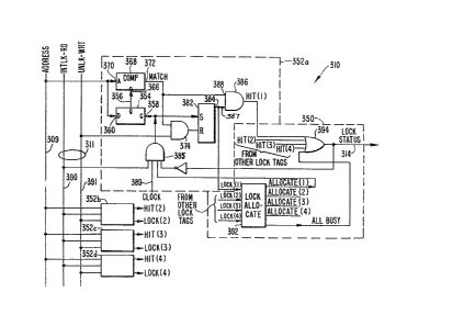
E. Description of Lock Controller 310
Referring now to Figure 9~ there is shown a more
detailed diagram of lock controller 310. In accordance wi-th
the invention the lock mean~ includes lock tag means for
receiving a selected address corresponding to an address in
memory array 39 to which an interlock read command ls to be
prevented. As embodied herein, the lock tag means include four
lock tags 352a, 352b, 352c, and 352d which, toget3er with a
logic controller ~ , consti-tu-te lock controller ~. It is
to be understood that more or Eewer lock tags could be provided
depending on khe specifia application. Lock tags 352a-d are
identical in construction and operation. For purposes of clar-
ity, detail.ed circuitry is shown only for lock tag 352a.
Each lock tag 352a-d includes a storage register 354
for storing a value corresponding to a location in address
space of system 20. Register 354 includes an output terminal
356 at which appears the value stored in register 354. Regis-
ter 354 includes an enable terminal 358 and an input -terminal
360 connected to address line 309. Activation of enable termi-
nal 358 causes register 354 to load the siynals presen~ on
address lines 309.
~3~
66~22 60
Register output terminal 356 is connecte~ to one inpu-t
terminal 366 of a comparator 368. Comparator 368 has another
input ~erminal 370 connected to address lines 309. An output
terminal 372 of comparator 368 constitutes a "match" signal which
is supplied to one input terminal of a -two-input AND gate 374~
The other input terminal of AND gate 374 is connected to unlock
write line 380 of command lines 311, The output -terminal of AND
gate 374 is connected to the reset terminal of a latch 3820 The
output terminal 384 of latch 382 constitutes a LOCK signal which
is supplied to one input terminal 387 of a two-input AND gate 386.
The other input terminal 388 of AND gate 38~ is connected to the
match signal output of comparator 368. The output of AND gate 386
constitutes a "hit" signal indicating that an address appearing on
address lines 309 is "locked" by lock tag 352a.
The Einal component of a lock tag 352a is a four-input
AND gate 385. One inpu-t of AND gate 385 is connected to a line
390 o~ command lines 311 indicatlng the command currently being
processed by memory node 39 is an interLock read command. A
second input of AND gate 385 is connected to a clock slgnal 38~ to
properly gate the operation of lock tag 352a and prevent race
conditions. A third input of AND gate 385 is connected to an
"allocate" ter~inal o~ logic controller 350 to be described below.
The fourth input terminal of AND gate 385 is connected to an
inverted lock status signal 314. The output -terminal of AND gate
385 is connected to the enable input 358 of register 354 and the
set terminal of latch 382.
Logic controller 350 includes a lock tag allocation
-26-
~.3~4~
~22-~
circuit 392 which functions as a selection encoder to select an
idle lock tag. Allocation circuit 392 deterrnines, by the status
of lock bits from lock tags 352a-d, which lock tags are free and
assigns one of the available lock tags to provide the locking
function by raising an "allocate" signal for the selected lock
tag. If all lock tags are currently assigned, an "all busy"
output signal is supplied to one input oE a five-input OR gate
394. The other inputs of OR gate 394 are supplied by -r0spective
"hit" signals of lock tags 352a-d.
-26a-
13~4~67
66~22-60
The operation o~ lock con~roller 310 ~o process an
interlock read command will now be described~ Address values on
address lines 309 ara constantly compared to stored a~dre~æ v~lue~
in registers 35~ none of the address values stored in
reglsters 354 1B equal to the addre~s value~ appearlny on addre~s
lines 309, no match signal is asserted, and no "hit" slgnal is
asserted. Assuming that the "all busy~ signal o~ circuit 392 is
also not asserted, no input of OR gate 394 i~ active and lock
status line 314 is not set. Memory axray 312 (Fig. 8) then
supplies the ~ontents of the ~peci~ied location to response
genera~or 316. The nonasser~ion of lock statu~ line 314 cause~
responsa generator 316 to yenerate the first type o~ response
message in which a "good read data" code is set in the bits of ~he
response message which will even~ually be kransmitted over
function ltnes of bus 25 to the commander node which requested
them.
The inverted value of lock ~atus line 314 is now
supplied to AND gate 385. Circuit 392 is ~upplying one o~ the
allocate slgnals of loc~ tags 352a-d. Since an interloak xead i5
being processed, interlock read line 390 is ~et by decodex 308
(Flg 8). Thus, when clock signal 389 is activated, AND ga~e 38S
of lock kag 352a is actl:vated ko enable reglster 354. The addresæ
value~ appearing on addres~ linas 309 are stored in regieter 354
of ~ock tag 352a. Activation O:e AND ~ate 385 al~o sets latah 382,
thus assertlng the output 334 which conskitutes a lock bik of lock
tag 352a. Acaeæ~ to the ~peci~ied loaation con~ained in regi~ter
354 of lock kay 352 is now de~led to ~ubsequent interlock read
commands.
A subæequent interlocX read com~and to the locked
location will result in the following operation. Addreæs values
appearing on address lines 309 are equal to the value stored in
reglster 354 of lock tag 352~. The ~atch signal a~ ter~inal 372
o~ lock tag 352~ is thus set. Since the lock bit at terminal 384
~or lock tag 352a i~ æek from the previou~ interlock read
operakion, ~oth lnput~ of AND gate 386 are now ac~ive, causlng ~he
27
.
~.3~ l67
668~2-6~
hit siynal of lock tag 352a to be asserted. This in turn
activates OR gate 394 to actlvate loak status line 314.
Actlvation of lock status line 314 aause~ response generator
27~
A
~28-
316 ~Figure 8) to generate a response message o~ a ~econd type
in which a ~CCKED response code is set on function bits of the
message.
The operation o~ a unlock write command to clear a
lock bit will now be described. An unlock write command -to a
location previously locked will result in the values present on
address lines 309 being equal to a value s'ored in a regis-ter
354 of a lock tag. For example, assume that an unlock write
command has been transmitted to unlock a location locked by
lock tag 352a. When the address value appears on address lines
309, the output of comparator 368 will cause a match signal to
be set. Since the unlock write line 391 will also be high at
this time, AND gate 374 will be activated, causiny latch 382 to
reset the lock bit signal at output terminal 384. AND gate 386
will be deactivated removing the active hit signal for lock tag
352a from the input terminal of OR gate 394. The data trans-
mitted with the unlock write command is then writ-ten into the
specified location in memory.
~ y providing a lock status message supplied to a pro-
cessor as a data transfer over the system bus at an unspeci~ied
time after an interlock read command, the present inven-tion
allows the functions o transfer acknowledge and lock status
transmission to be separated, thereby providing for the use of
multiple lock bits without the expense and complexity which
would be required if lock status information were required to
be transmitted at a predetermined time or over dedicated lock
status lines. This also permits lock status inEormation to be
obtained ~rom nodes connected to the system -through adapters
and buses separate Erom the system bus.
Throughout the previous discussion, locked memory, or
address space, was said to be specified by a "location." It is
to be understood that each address stored register may consti-
tute a range of addresses, such that a single interlock read
command or unlock write command can respectively lock and
unlock a range of locations in address, and not merely a sinyle
location.
It will be apparent to those skilled in the art that
various modifications and variations can be made in the bus
13~6~
interface circui-try and interfa~e oE this inven-tion without
departing from the spirit or scope of the present invention.
The present invention covers such modifications and vari~tions
which are wi-thin the scope of the appended claims and -their
equivalents.
..... . .. . ..