Note: Descriptions are shown in the official language in which they were submitted.
~ ~l3~L4~;~
PHF 87.573 1 1 September 19~8
"Circuit for recovering the carrier in digital transmission systems.
The in~ention relates to a circuit for recovering the
carrier of a digitally modulated wave having a phase symmetry 2~/M,
where M is the symmetry order of the constellation of the states,
including means ~or fast automatic acquisition comprising a voltage-
controlled oscillator having an output supplying said carrier and acontrol input to which an error signal ~(~) is applied in order to
change the oscillator phase and adjust it to the phase of said
digitally modulated wave, said wave being in~roduced:
. into a first channel comprising the series arrangement of:
- a demodulator receiving the modulated wave and the oscillator output
signal, the demodulator being followed by a low-pass filter which
produces a filtered signal X,
. into a second channel comprising the series arrangement of:
- a phase shifter for shifting the phase of the oscillator signal
through 9O
- a demodulator receiving the modula~ed wave and the phase shifter
output signal, the demodulator being followed by a low-pass filter
which produces a filtered signal Y,
the two channels with a basic clock H (recovered clock symbol) entering
a phase comparator arrangement, which determines a comparator signal
and validates same.with the aid of a variable rate sampling clock which
reproduces the basic clock H by discarding certain edges, the comparator
signal being stored and then introduced into an amplifying filter which
produces the oscillator control error signal (~), the graphic
representation of the states of a signal constellation being defined in
polar coordinates by the function F(A,0) where A is the amplitude and
0 the phase of each signal point of the constellation, and ~ being
the phase difference between the received ~odulated wave and the
corresponding signal poi~t constella~ion.
The invention also relates to the arrangements in which a
carrier recovery circuit is used, such as digital transmission
arrangements, more specifically, those arrange~ents in which digital
" ~3(1~50
PHF 87.573 2 1 September 1988
information, after being transmitted by ~odulation of an electro-
magnetic wave, is recovered by coherent demodulation. These arrangements
are employed in data transmission modems, ~icrowave radio links, space
or optical communications systems for heterodyne links.
For effecting the coherent demodulation, the phase of the
carrier is generally recovered with the aid of an oscillator included in
a carrier recovery loop. The voltage of this oscillator is controlled by
a filtered version of the output signal of a phase comparator which
detects the phase error between the oscillator and the transmission
carrier.
For digital modulation schemes having a large number of
states, the phase difference between the oscillator and the carrier must
of necessity be li~ited to small values. The noise bandwidth of the
recovery loop is then reduced by means of narrow-band low-pass
filtering. This reduction results in very low phase noise, and also in a
considerable decrease of the acquisition range. To off-set this
disadvantage, auxiliary arrangements are used for assisting in the
acquisition.
Among these auxiliar arrangements frequency
descriminators are currently used which generate a voltage depending on
the frequency difference between the oscillator and the carrier, as
described in, for example, French Patent Specification No. 2 552 959,
published 25 October 1985. This Specification relates to a carrier
recovery circuit for digital modulation sche~es having a phase symmetry
2~/M, in which circuit a variable-rate sampling of the out.put signal of
the phase co~parator changes the latter into a frequency discriminator.
This property is obtained by eliminating zero-crossings of the ~hase
comparator output which occur when the phase error between the
oscillator and the carrier is equal to ~/M ~ 2k~/M, where k and M are
integers.
Well, in view of multi-state digital amplitude
modulations of two quadrature carriers, the frequency discriminator
described in the aboYe-~entioned Specification has dra~backs because its
gain is degraded, for at the sampled output of the phase comparator ~ero-
crossings occur which are ta~en into account, but do not correspond to azero phase error. Actually, starting fro~ a basic clock H, this
frequency discriminator generates a sampling clock, in which certain
: . ,
''
~3~49L51~
PHF 87.573 3 1 September 1988
active edges of this basic clock H are eliminated. This eli~ination
occurs when zero-crossings are detected for which the phase difference
between the oscillator and the carrier wave is equal to ~ ~ 2k~
M M
~ut experience has shown that, in phase and amplitude
modulations, there are other zero-crossings at the output of the phase
comparator which corrupt a correct acquisition of the carrier. For
example, in the case of 16 QAM modulation, the outputs of the currently
used phase comparators have zero-crossings when the phase difference is
10 equal to ~ = arc tan (1/3) for the states (3,1), (-1,3), (-3,-1),
(1,-3). Other states show a similar behaviour. In addition, in the case
of a more important number of modulation states, the number of these
unwanted zero-crossings will grow, and this causes a deterioration of
the performance of ~he discriminator.
Therefore, the invention has for its object to obviate
this degradation by avoiding that all these unwanted zero-crossings are
taken account of.
Thereto, the invention as set forth in the opening
paragraph is characterized in that the carrier recovery circuit
comprises a phase comparator arrangement which operates alternately as
a phase detector and as a frequency detector and therefore comprises
means for selecting received signal points with the aid of selection
zones located around certain states of the signal constellation, the
zones forming ring segments and being determined by the intersection:
- first, of the angular sections (-~ ) corresponding to a phase
difference ~ between the received modulated wave and the
corresponding signal point of the constellation, such that the
absolute ~alue of ~ is less than ~ where ~ is a preset boundary,
each ~ection having a symmetry axis passing through the diagonal
states of the signal constellation, these zones being situated
around the diagonal states of the signal constellation for which
zones in a quarter of the plane there is only a single state
having a given amplitude A,
- secondly, of the boundary circles, centered at the origia of the
signal constellation, of radius ~ , the circles
being equidistant from two consecutive circles that join the states
together, the one passing through the states at the constant
~IL3~gL4S(:~
PHF 87.573 4 1 September 1988
amplitude Al and the other passing through the states at the
consecutive constant amplitude A2, thus forming rings, the point of
origin forming the innermost circle, the outside boundary (circle)
being restricted by the maximum amplitude of the detected signal,
the arrangement further including sampling clock generating ~eans which
in the acquisition mode (off-hook), validate the basic clock H only for
these selected zones and which, in the permanent mode (on-hook),
validate all the edges of the clock H for forming the sampling clock.
When states of the constellation have a minimum angle
between two adjacent states in the same circle of less than ~/2, the
phase difference such as the absolute value of ~ < ~ is taken into
account, this means that the zone is selected when the signs of the
phase difference are the same for the two adjacent states.
For selecting the zones, the data X and Y are used to
address a memory which contains the information belonging to or not
belonging to the signal point received in one of the selected zones as
well as the amplitude and the sign of the error which relate thereto.
This circuit is based on storing the error signal when
the absolute value of the phase difference ~ exceeds a certain value.
This storing is effected in bistable triggers whose output data remain
constant between two valid, recognized zero-crossings. This error signal
provides information on the sign of the frequency difference between the
oscillator and the carrier. This storing is effected when the phase
difference at the output of the comparator is situated within the
defined selection zones.
This carrier recovery circuit utilizes a phase comparator
having the following properties:
- its characteristic becomes zero at the occurrence of a zero phase
error;
- its characteristic has the periodicity of 2~/M, where M is the
symmetry order of the modulation.
The invention is used for digital modulation schemes
having a phase sym~et~y 2~/M, where ~ is the symmetry order of the
signal constellation. Thus, a 4-state phase modulation has a symmetry of
the order of 4, for an 8-state phase modulation the symmetry is of the
order of 8, for a 16 QAM modulation (phase and amplitude modulation by
means of amplitude modulation of two quadrature carriers) the symmetrY
~L31D~S~
PHF 87.573 5 1 Septemher 1988
is of the order of 4.
But the invention presents its determining advantages in
the case of an a~plitude and phase modulation in a great number of
states, of the 2n type ~n = integer), for example, 64 QAM, 256 QAM. It
also presents advantages in the case of amplitude and phase modulations
for ~hich the phase differences between certain signal points of the
signal constellation are less than the symmetry 2~/~. Thus, in 64 Q~M
modulation the symmetry is ~/2, but the phase difference between the
states (+1, ~1) and (+1, ~5) is ~/4-arc tan (1/5), thus less than ~/2.
During the caxrier acquisition period, the digitally
modulated wave will be able to present all the signal points of the
signal constellation. Consequently, the invention cancels all the
received signal points liable to cause a faulty acquisition and uses
only the points that are liable to cause a correct acquisition.
Thus, the carrier recovery circuit according to the
invention includes means for selecting the received signal points with
the aid of zones situated around certain states of the signal
constellation.
This selection is effected by determining whether the
received signal points belong or do not belong to zones for which any
received signal point in these zones presents a phase difference with
the transmitted signal point, such that the absolute value of this phase
difference remains below, except for 2k~/M, a predetermined value, which
renders it possible to eliminate the zero-crossings at k~/M.
Thus, the phase information taken into account is only
the information supplied by the received signal points in these zones.
To determine whether these points belong to these zones, and thereafter
taking account of the information assignable thereto, the invention
provides a phase comparator arrangement that can be inserted in a
carrier recovery circuit. For that purpose, the digitally modulated wave
is slmultaneously fed into two demodulators, which also receive the
output signal o~ the oscillator, one directly and the-other through a
~/2 phase shifter, and produce the de~odulated signals X1 and Y1,
re~pecti~ely. These demodulated signals are filtered and provide the
respective signals X (in-phase) and Y (quadrature). The signals X and Y
are fed into the phase comparator arrangement and are used to address a
memory. The data ~ and Y are encoded in a certain number of bits
- 6 - 20104-8473
depending on the precision with which the selection zones are to
be determined.
The phase comparator arrangement comprises two analog-
to-digital converters inserted in the in-phase channel and
quadrature channel, respectively, so as to receive the cartesian
coordinates X and Y of the received signal point, the two conver-
ters supplying data that address a memory whose output supplies
_ bits, one of the bits being a bit belonging to the received
signal point in one of the selection zones which activates an input
of a logic OR gate whose other input receives an external on-hook/
off-hook signal, the output signal of the OR gate entering an AND
gate with the basic clock H so as to suppress the edges when, in
the acquisition mode, the received signal point is not present
in a selection zone, and to validate all the edges in the permanent
state, in order to form the sampling clock which activates p-l
bistable triggers that receive the p-l bits from the memory, the
output signals of the bistable triggers driving a digital-to-
analog converter which delivers the error signal that acts on the
oscillator through the amplifying filter.
Stated another way, the invention may be summarized as
a circuit for recovering a carrier from a digitally modulated wave
having a phase symmetry 2 ~/M, where M is an integer representing
a symmetry order of a modulation scheme of said digitally modulated
signal, said modulation scheme corresponding to a signal constel-
lation hav1ng states, which states are representable using a
graphic representation in polar coordinates by a function F(A,~),
Q
~ ~;2,
~,
~30~9L5~
- 6a - 20104-~473
where A and ~ represent modulus and phase, respectively, of the
states in the signal constellation, the circuit comprising:
(a) a voltage-controlled oscillator having an output for
supplying an output signal which represents said carrier and a
control input for receiving an error signal ~(~) for changing a
phase of the oscillator to adjust it to a phase of said digitally
modulated wave, the phase ~ being the phase difference between
signal points of received digitally modulated wave and correspond-
ing states, idealized ones of said signal points being states of
said signal constellation;
(b) a first channel for in-phase demodulation;
(c) a second channel for quadrature-phase demodulation;
(d) phase comparing means, coupled to outputs of the first
and second channels and to receive a basic recovered clock signal
H, for determining and validating a comparator signal, the phase
comparing means alternatively operating as phase detector and as
a frequency detector and comprising means for selecting received
signal points using selection zones, said selection zones being
defined with respect to said graphic representation as located
around certain states of the signal constellation, said selection
zones appearing in said graphic representation as ring segments;
(e) means for producing a variable rate sampling clock
signal which reproduces the basic clock signal H by discarding
certain edges, said producing means:
~i) when the circuit is in acquisition mode (unlocked),
: ~ validating the basic clock signal H only for the selection zone;
~L3~15~
- 6b - 20104-8473
and
(ii) when the circuit is in permanent mode (locked),
validating all edges of the clock signal H for forming the sampling
clock signal;
said sampling clock signal being supplied to the comparing means
to control validating of the comparator signal; and
(f) means for converting the comparator signal to the error
signal ~
The invention and how it can be put into effect will
be better understood from the following description given by way
of non-limitative example with reference to the accompanying
drawings, in which:
Figure 1: shows, in a quarter plane, the 64 QAM signal
constellation in which the selection zones according to the
invention are represented in the case of a predetermined boundary
< 18.92j
Figure 2: shows a signal constellation analogous to that
of Figure 1 for 18.92< ~ ~ 22.62,
Figure 3: shows a signal constellation analogous to
that of Figure 1 for 22.52< ~ < 28.07,
Figure 4: shows a block diagram of the carrier recovery
circuit according to the invention,
Figure 5 shows the phase comparator characteristic and
variations in the phase of the comparator output signal before
and after storage in a bistable trigger.
Figure 1 shows in a quarter plane the 16 states of a 64
QAM wave. For the overall plane this system has a phase symmetry
2 ~/M = ~/2.
" ~ . . .
13Q~
PHF 87.573 7 1 September 1988
In accordance with the phase variation of the incoming modulated wa~e
relative to the oscillator, for a specific state of the signal
constellation, the received signal point will shift through a circle
centered at O passing through the specific state or the viscinity of
this specific state.
~ etween two states of module A1 and A2, the modules A1
and A2 being consecutive, for example the states (3,3) and (5,1), a
boundary circle 40 is defined equidistant from the t~o states such that
its radius is A1 2 A2 This permits to de~ine the zones
belonging to the two states as a function of their respective module,
and to define rings passing through all the states having the same
module. Inside these rings a signal point of whatever phase may be
received and situated on either one side of the state of the signal
constellation, which defines a phase difference. The positive sign is
effected if the phase of the received signal point is higher than that
of the constellation point and vice versa . Subsequently, a
subdivision is effected into polar coordinates of the overall plane of
the constellation. A rotation in either direction characterizes the sign
of the phase difference.
The invention defines a boundary ~ for the phase
difference ~ beyond ~hich the received signal point is no longer used
for synchronizing the local carrier of the recovery circuit with the
transmitted carrier. The zones that are determined by the invention are
thus bounded by the bounding circles and by the section (-~, +~). Thus,
around the state (3,3) there is a selection zone, provided with a
negative sign, bounded by the bounding circles 40 and 31 and the
segments 32 and 34. There is al50 a selection zone with a positive si~n
bounded by the same bounding circles and by the segments 33 and 34.
This occurs in the same fashion for the states t1,1) and
(7,7) with the following characteristic features. For the state (1,1)
the internal bounding circle is constituted by the origin. ~or the state
(7.7) the external bounding circle i5 not defined, the boundary being
constituted by the ~xi~um ampl}tude of the received signal point.
~he states (+ 1, + 1), (+ 3, + 3),
(+ 7, + 7) have an equal symmetry at ~/2 for the overall 64 QAM
signal constellation. Thus, they are certainly determined in a quarter
plane of the signal constellation. On the other hand, there is in a
~3~4~i~
PHF 87.573 8 1 September 1988
quarter plane a diagonal state (+5, ~5) which has a symmetry lower than
~J2 and thus cannot be distinguished from the states t-~7, +1) and
(+1, +7). Thus, in the ring passing through these three states there are
not any selection zones.
The invention thus determines three selection zones
situated in the rings defined around diagonal states (1,1), (3,3),
(7,7). They are shown in Fig. 1 by hatched areas. The incoming signal
shown in cartesian data along X and Y, allows to determine whether the
received signal point belongs or does not belong to one of these zones.
The data along X and Y are encoded over several bits in accordance with
the desired precision. If the received signal point is situated in a
section of the selection zone, such as 35, it will be provided with sign
information (here the negative sign) and amplitude information
characterizing, if need be, its distance relative to the state (3,3), in
order to produce the adequate phase correction. A simple encoding can be
constituted by two bits, one for the sign and the other for the
amplitude of the correction, thus constant for the whole zone.
A more elaborate encoding can be formed by three bits,
one for the sign and the other two bits for defining several correction
amplitudes according to the position of signal point 35 within the
selection zone.
This encoding is effected for all the selection zones.
The boundaries ~ can otherwise be different for each of the zones.
Fig. 2 shows the same situation as that of Fig. 1 but
with a more important boundary ~. In this case, starting from the state
(+5, +7) for example, a section is shown corresponding with the phase
difference ~ defining the segment 41 which constitutes the range of
the zone with the negative sign belonging to state (5, 7). This zone is
superposed on the zone with the negative sign belonging to the state
(7, 5). When the two phase difference æones having a negative sign cover
each other, and every received signal point is situated in the hatched
area 42, the sign of the correction is determined unambiguously. Because
of the symmetEy ~ne 43 belongs to the state (5, 7) with a positive
correction. The two selection zones 42 and 43 can thus be used for
determining the sign of the phase difference ~ when the value ~ exceeds
2~45 - arc tan (5J7)] = 18.92, that is to say when the negative
zone belonging to the state (5, 7) covers the negative zone belonging to
~44~
PHF 87.573 9 1 September 1988
the state (7, 5).
Fig. 3 shows the same situation as that of Fig. 2 but
with an even more important boundary ~. Actually, when ~ reaches
2 arc tan (1/5) = 22.62, new selection zones 51, 52 belonging to the
states (5, 1) and (1, 5) will appear in the same way as in the preceding
case.
Thus, for the quarter plane, when ~ < 18.92, the
selection zones that are suitable for use are shown in Fig. 1. When
18.92 < ~ < 22.62, the selection zones that are suitable for
use are ~hown in Fig. 2. When 22.62 ~ ~ < 28.07 =
2[45 - arc tan (3/5)] the selection zones that are suitable for use
are shown in Fig. 3.
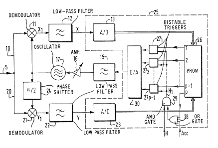
Fig. 4 shows the block diagram of the carrier recovery
circuit. The digitally modulated wave arrives at the input terminal 5
and biffercates into two channels 10 and 20 which are in phase and in
quadrature, respectively, with the wave from the oscillator 17. This
oscillator applies its signal directly to the demodulator 11 of the in-
phase channel and also to the demodulator 21 in the quadrature channel
Ql~ the ~/2 phase shifter 24. The output signals from the demodulators
11 and 21 are filtered in the respective low-pass filters 12 and 22,
whose output signals are the respective signals X and Y. These signals
penetrate into the phase comparator arrange~ent 25, or two analog-to-
digital converters 13, 23, respectively, which supply data addressing a
PROM memory 26. This memory delivers ~ bits of which p-1 bits are
stored in the bis~able triggers 271l 272 ... 27p-1- These p-1 bits
form a code of the sign and the amplitude of the estimated phase error.
The pth bit pp determines whether the received signal point
determined by the coordinates X, Y belongs to or does not belong to a
chosen selection zone. The pth bit enters an OR gate 28 which receives
a signal ACC determining ~hether the carrier recovery circuit is in the
permanent mode (on-hook) (ACC = 1) or in the acquisition mode (off-
hook) ~ACC = O). In fact, the recovery circuit according to the
invention operat~s as a per~nent ~ode (ACC = 1) phase detector. In the
acquisition mode (ACC = O) it operates as a frequency detector.
Therefore, the output signal of the logic OR gate 28 enters logic AND
gate 29 with the basic cloc~ H. Then the signal H1 at the output of
the logic AND gate 29 is the copy of the clock H when ACC = 1. On the
:,
~ ~L3~4SO
PHF 87.573 10 1 September 198
other hand, when ACC = O the edges are validated if pp = 1 and
suppressed if pp = O.
This signal H1 constitutes the clock for the bistable
triggers 271 to 27p_1. Thus, the p-1 bits that are produced by the
memory 26 at each clock pulse H are stored in the bistable triggers. The
latter keep their information for the duration when
ACC = O and pp = O.
All the output signals of the p-1 bistable triggers enter
a digital-to-analog converter 30 which supplies a signal that
passes through a low-pass filter 15 then through an amplifier 16 in
order to produce a control signal ~) that controls the oscillator 17.
Evidently, it will be possible to those skilled in the art to reverse
the logic state of the siqnals and, consequently, change the type of
logic gate used.
The characteristic feature of the phase comparator
arrangement 25 according to the invention is to be able to operate as a
frequency detector when ACC = O and as a phase detector when ACC = 1.
Fig. 5 shows in B the characteristic features of a phase
comparator for a phase comprised between ~ and +~tM. On either side
of signal point O (phase difference zero), the phase comparator supplies
a voltage as a function of the phase difference which allows to bring
the oscillator frequency under control. The output voltage cf the
comparator is represented in C. The mean value of this output voltage is
zero. For correcting the oscillator frequency, the value of the phase
difference is stored with the aid of a phase comparator arrangement that
chaxacterizes the invention. When the absolute value of the phase
difference exceeds the boundary ~, which corresponds with the enabling
of the chosen selection zone, the triggers latch the condition of the
output signal of the memory. Such a latched signal is shown in D; its
mean value is no longer zero. It permits to correct the oscillator
frequency. The curves C and D of Fig. 5 are representative of a positive
frequency difference, that i5 to say, a greater modulated carrier
frequency than t~e ~scLllat~r frequency. For a negative frequency
difference t~e curves C and D show an inverse trend.
.
,