Note: Descriptions are shown in the official language in which they were submitted.
~3~1~4457
NARROW RANGE DIGITAL CLOCK CIRCUIT
~ield of the Invention
This invention relates generally to a clock
circuit and more specifically to a digital phase locked loop
clock circuit in which a high speed circuit performs high
speed digital operations which emulate medium speed analog
components; the only non-digital component is a local crystal
oscillator.
Description of Pri~r Art
Phase locked loop circuits have been used for many
years. Prior art phase locked loop circuits are exemplified
in United States patents bearing numbers 4,498,059,
4,503,400, 4,748,644 and 4,724,402. They are often used in
clock circuits in the receivers of digital systems for the
purpose of synchronizing the local clock with the incoming
data signal. In the existing circuits, a voltage controlled
oscillator (VCXO) controlled by a digital to analog (D/A-
converter) is used as the local clock signal and forms a part
of the phase locked loop. The testing and adjustment of
these analog circuits tend to add significant cost in
addition to the expense of providing the additional power
supplies that they typically need. Conventional prio-r art
analog phase locked loop circuits also tend to suffer from
signal drift and signal degradation due mostly to the analog
components.
It is therefore an object of the invention to
provide an improved phase locked loop clock circuit which
eliminates the problems associated with the conventional
clock circuits. The circuit of the invention does not use
analog components other than a local crystal oscillator and
realizes the conventional medium speed VCXO and D/A-
converter functions with a high speed digital circuit. The
circuit of the invention requires less printed circuit board
space than the prior art circuits and no special power
supplies are needed.
~,~
~3Q144S7
Summary of ~he Invention
In accordance with the invention, there is provided a
digital clock circuit for providing an output clock signal
having a frequency varying between predetermine~ limits. The
circuit comprises a first input terminal for receiving a
fixed frequency signal, a second input terminal for receiving
a variable reference signal and an output terminal for
providing the output clock signal having substantially the
same frequency as the fixed frequency signal. A digital
~requency changer circuit is connected to the first input
terminal and is responsive to the fixed frequency signal and
to control signals for generating the output clock signal. A
circuit means is responsive to the variable reference signal
and to the output clock signal for generating a binary
control word representativa of a frequency difference
therebetween, the binary control word comprising a sign bit
and a plurality of other bits. A rate multiplier circuit is
responsive to the binary control word and the output clock
signal for generating the control signals.
From another aspect, the invention provides a
method of generating an output clocX signal having a
frequency varying between predetermined limits in a digital
clock circuit having a first input terminal for connection to
a fi~ed frequency signal, a second input terminal for
connection to a variable reference signal and an output
terminal for providing the output clock signal. The method
comprises the steps of receiving a fixed frequency signal on
the first input terminal, receiving a variable reference
signal on the second input terminal and generating a signed
binary control word representative of a frequency difference
between the output clock signal and the variable reference
signal. Control signals having a predetermined relationship
to the output clock signal and the signed binary control word
are generated and the output clock signal is maintained
between predetermined limits in response to the control
signals thereby tracking the variable reference signal.
From yet another aspect, the method of the
invention comprises the steps of receiving a fixed frequency
~3~45~
signal on a first input terminal, receiving a variable
reference signal on a second input terminal, generating
control signals representative of the frequency relationship
between the output clock signal and the variable reference
signal and, for every cycle of the fixed frequency signal,
digitally generating a cycle of the output clock signal
having a similar frequency characteristic to that of the last
completed cycle of the fixed frequency signal or lengthened
or shortened by a fractional increment of the fixed frequency
signal in dependence upon the control signals.
The present invention provides a clock circuit
which is more economical than functionally equivalent prior
art circuits and requires less real estate on a printed
circuit board; space efficient digital components replace
bulky, heavy and costly analog components of con~entional
prior art circuits.
Brief Description of the Dra~ings
An embodiment of the invention will now be
described with reference to the accompanying drawings in
which:
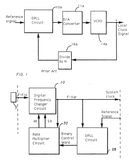
Figure 1 is a block diagram of a typical prior art
analog phase locked loop clock circuit;
Figure 2 is a block diagram of a digital phase
locked 1GOP clock circuit in accordance with the invention;
Figure 3 is a detailed block diagram of the
digital frequency changer circuit illustrated in figure 2;
Figure 4 is a detailed block diagram of the data
manipulation circuit illustrated in figure 3;
Figure 5 is a detailed block diagram of the rate
multiplier circuit illustrated in figure 2;
Figure 6a is a timing diagram illustrating a first
mode of operation of the circuit of figure 2;
Figure 6b is a timing diagram illustrating a
second mode of operation of the circuit of figure 2; and
Figure 6c is a ~iming diagram illustrating a third
mode of operation of the circuit of figure 2.
~3 1:)4~S7
Description o-f the Pre~erred Embodiment
Referring now to the prior art circuit of
figure 1, a VCXO 14a is adapted to provide a local clock
signal on an output terminal X for use by electronic
circuitry connected to that terminal. The output signal of
the VCXO is scaled using a divide by N circuit 16a and fed
back to a phase comparator and DPLL algorithm circuit lOa.
The circuit lOa is also connected to a variable reference
signal source and is adapted to provide a signal
representative of the phase relationship between the variable
reference signal and the feedback scaled local clock signal
to a D/A-converter lla. The circuit lOa conventionally uses
a microprocessor as its local intelligence to perform a
Digital Phase Locked Loop (DPLL~ algorithm on the phase
difference of two incoming signals. According to present and
historical phase values measured, the DPLL circuit supplies a
digital value to the D/A-converter lla which convarts it to
an analog voltaye supplied to the VCXO 14a.
Figure 2 illustrates a fully digital clock circuit
in accordance with the present invention. There is shown a
digital frequency changer circuit (DFC) 10 having a first
input terminal connected to a fixed frequency ~ignal source
such as a crystal oscillator 5 and a pair of other input
terminals respectively connected to receive HI and LO control
z5 signals from a rate multiplier circuit 30. The output
terminal of the DFC 10 is connected to a system clock output
terminal as well as to an input terminal of the rate
multiplier circuit ~0 and to a phase comparator and DPLL
1 algorithm circuit ~. DPLL circuits are well known in the
art and an example can be found in IEEE Transactions on
Communications Vol. COM 31 No.12, December 1983 in the
article: "Intelligent PLL using Digital Processing for
Metwork Synchronization" by H.Fukinuki and I. Furukawa. The
DPLL circuit 50 may also be connected to a source of control
signals (not shown) and to an input terminal for receiving a
variable reference signal as described later. The reference
signal may, for example, originate from a master clock
circuit adapted to provide reference signals to a plurality
~3~ S7
of subsystems each provided with a respective clock circuit.
As all signals normally do, the reference signal tends to
vary between predetermined limits and it is a desired object
of this circuit that the output clock signal track the
reference signal while providing an output signal having a
frequency substantially the same as the fixed frequency
signal source.
The DFC 10 is a high speed digital circuit that
performs, in a digital manner, functions that are performed
with analog components in conventional clock circuits. In
view of its relatively high speed requirements, this circuit
may be realized with a gallium arsenide integrated circuit.
The rate multiplier circuit 30 and the DPLL ~ have a lower
speed requirement than the DFC 10 and may be realized using
more conventional integrated circuit technology. The crystal
oscillator 5 may be any conventional oscillator adapted to
provide a nominal fixed frequency signal with a predetermined
stability.
In operation, the DFC 10 is responsive to the
fixed frequency signal F-Fix and to the HI-L0 control signals
to provide an output clock signal F-Var on the system cloc~
output terminal The F-Var signal is also applied to the
DPLL circuit ~ and to the rate multiplier circuit 30. The
DPLL circuit ~ is responsive to the output signal F-Var, and
~5 to the variable reference signal t~ provide a binary control
word to the rate multiplier circuit 30. The binary control
word represents the frequency difference between the fixed
frequency signal and the signal F-Var. The DPLL circuit 50
integrates over time the phase difference between the signal
F-Var and the variable reference signal to generate the
binary control word. The rate multiplier circuit 30 is
responsive to the signal F-Var and to the binary control
word, to provide the control signals HI and L0 to the DFC 10.
Under normal operational conditions, the frequency of the F-
Var signal is allowed to vary up or down but only betweenvery narrow predetermined limits as described later. In an
alternate operating mode as dictated by appropriate control
signals, the DPLL circuit 50 may be controlled to operate in
~L3~45i7
a test mode whereby the circuit may be exercised to ascertain
that it is operating correctly.
Figure 3 illustrates the DFC 10 and is partitioned
into a period measurement section 50, a period synthesis
section 55, and a square wave generating section 60 as well
as a local oscillator 6 which may be a commercially available
circuit adapted to provide a high frequency local clock
signal F-Loc. As will become evident Erom the following
description, the frequency of F-Loc must be selected to be
much greater than the frequency of F-Fix; the granularity of
frequency adjustment is dependent on the ratio of these two
signals.
The period measurement section 50 includes an edge
discriminator 12 having a first input terminal connected to
receive the fixed frequency signal F-Fix and its output
terminal connected to a counter 14 and a latch 16. The edge
discriminator 12 is also connected to receive the high
frequency clock signal F-Loc. The edge discriminator may
conveniently be an edge sensitive triggerable flip-flop.
In operation, the period measurement circuit is
responsive to the input signals F-Fix and F-Loc respectively
for producing a binary value N which reflects the frequency
relationship between the signals F-Fix and F-Loc, such that N
= F-Loc . F-Fix, where N is an integPr equal or greater than
2. N may vary by 1 unit when F-Fix is not an exact
submultiple of F-Loc. The edge discriminator 12 performs the
synchronous differentiation of one edge of the signal F-Fix
with the signal F-Loc. The output of the edge discriminator
is a periodic signal which is used to reset the first counter
14 and to load the latch 16 in coincidence with the input
clock siynal F-Loc. The counter 14 increases its count by
one unit for each period of the F-Loc clock signal and on
reset, its current count is stored in the latch 16 yielding
the value N. The signal M which is the bit inverse value of
N is available at the output of inverter circuit 17. The
input edges of the F-Fix clock pulses are sampled (quantized)
to the nearest period of F-Loc, and the value N reflects the
last period sampled. Of course, the counter 14 and the latch
~3~)~L457
16 must be large enough to count and store the integer N.
The period synthesis section in figure 3 includes
a second counter 18 having an input clock signal F-Loc. The
counter 18 provides a group o~ output signals R in response
to a preload signal, the signal F-Loc and the signal M. Upon
assertion of the preload signal the counter 18 loads the
value M. The period synthesis section further includes a
decode circuit 20 responsive to the signal R for providing a
decoded output signal D61. A 3-bit shift register 22 is
responsive to the signal D61 and to the signal F-Loc for
providing the preload signal via logic gates 25, 26, 27 and
28 which are also controlled by the HI-LO control signals.
In the ensuing descriptions of operati~n,
reference may conveniently be mada to figures 6a, 6b, and 6c
which are timing diagrams illustrating the operation of the
circuit in three possible modes. In the illustratad example,
the local clock signal F-Loc has a nominal frequency of one
gigahertz and the F-Fix signal has a frequency of 40
megahertz. A11 the counters and the latch 16 are six bits
wide. The amount of jitter that is present on the output
clock signal F-Var is inversely proportional to the signal F-
Loc.
In operation, the second counter 18 counts input
clock pulses F-Loc but is preset to a value M which is the
bit inverse of N. The counter 18 resets itself each time it
reaches a full count. The decode circuit 20 is responsive to
the output signals R of the second counter 18 to provide an
output signal D61 which anticipates a full count of the
second counter 18 by three clock cycles. For example the
decode value of '-3' (equivalent to a value of 61 or the
binary value 111101 using 6-bit registers and counters)
provides the 3-bit shift register 22 with the input signal
D6l from the decoder 20 which is three clock cycles early.
The 3-bit ~hift register 22 thus provides three output
signals D-LO, D-NORM and D-HI which are delayed one, two and
three clock cycles respectively, relative to the output
signal D61 of the decode circuit 20. The D-NORM signal
corresponds to the desired nominal frequency of the output
~L3~14~57
clock signal F-Var. It also serves as the preset input to
the output stags of the DFC 10. The choice of using D-NORM
as the preset input is arbitrary and either of the signals D-
LO or D-HI can also be used instead of D-NORM. The gate 25
has an output signal OUTl corresponding to a logical ~ND
operation performed on its input signals ~-LO and the control
signal LO (D-LO LO)o Gate 26 has an output signal OUT2
corresponding to a logical AND operation performed on its
input signals D-NORM~ and the control signals HI and Lo both
inverted (D-NORM ~I Lo). The gate 27 has an output
signal OUT3 corresponding to a logical AND operation
performed on its input signals D-HI and the control signal HI
(D-HI HI)o The OR gate 28 is responsive to the output
signals OUTl, OUT2, and OUT3 to provide the preload signal to
the counter 18. AS illustrated in figures 6a, 6b,and 6c the
selection of D-HI, D-NORM or D-LO results in the generation
of the output signal F-Var with a period shorter, the same or
longer than F-Fix. Varying the synthesized period by +/- 1
from nominal, effectively moves an output edge forward or
backward by 1 nsec (given the example of a lGhz local
oscillator). Thus, selecting D-NORM and occasionally varying
D-HI or D-LO for one cycle of the counter, effects an
arbitrarily small effective frequency offset from F-Fix, yet
still not introducing more than l nanosecond of jitter in the
output signal F-Var.
The square wave generation section 60 includes a
data manipulation logic circuit 45 responsive to the input
signals M, to provide an output signal Sl to a third counter
24. As shown in figure ~, the data manipulation circuit 45
may be realized using a pair of registers interconnected as
illustrated. The circuit 45 manipulates the input signal M
(J bits wide~ first by dropping the least significant bit
(LSB) to generate a signal which is J-l bits wide. A signal
having the value of logic l is then concatenated at the most
significant bit position (MSB) with that signal to yield a
new mapped signal Sl which is also J bits wide. For example
if J = 6 and M = 110001~ dropping the LSB yields llOOO and
concatenating a 1 to the M5B yields 111000.
~L304457
The countPr 24 has an output terminal that
corresponds to its most significant stage and is responsive
to the clock input signal F-Loc, and to the preset signal
from shift register 2~ to generate the square wave output
signal F-Var.
Figure 5 illustrates the medium speed rate
multiplier circuit 30 of figure 2. It includes a binary
adder 32, an accumulator register 34, an edge discriminator
36 and steering logic 70. These circuit elements may be
realized using commercially available off-the-shelf
components. The multiplier circuit converts a signed binary
control word C from the DPLL circuit ~ into evenly spaced HI
or LO pulses. The binary k-bit adder 32 provides an output
signal S2 comprised of a plurality of bits (k-bits, the kth
bit being the most significant bit) in response to signal S3
and the control word C comprised of a 2's complement k-bit
control word exclusive of the sign bit. The accumulator
register 34 is responsive to the clock input signal F-Var and
to the output signal S2 of the binary adder 32 to generate
the k-bit output signal S3. The edge discriminator 36 is
responsive to the clock input signal F-Var and to a one bit
wide input signal comprising the kth bit of the group of
signals S3 of the accumulator register 34 to provide a
control signal S4 corresponding to the differentiated kth bit
of the accumulator output signal S3. The output signal S4 is
a pulse occurring at the rate of the absolute value of C
pulses in 2**k clock periods. This pulse is directed to the
HI or LO inputs of the DFC circuit 10 via the steering logic
70. Depending on the sign bit of signal C, the steeriny
logic 70 assert~ one of the HI and LO signals using gates
40, and 42. For example, with the value oP C = O, the
accumulator value does not change, and HI or LO pulses are
not generated and F-Var = F-Fix. With a 16 bit accumulator
and the value of C = 3, the sign bit being positive, three
pulses in 64k pulses occur at the Hi output kerminal. When
C = -1, one pulse in 64k clocks occurs at the LO output
terminal. With a lGhz local oscillator F-Loc and with an
incoming clock signal F-Fix = 4OMhz, F-Var = F-Fix +/-
:`
~30~57
0.625ppm (parts per million), a step size comparable to thatobtained with the counterpart analog solution for stratum 4
clocks using a D/A converter and a VCXO.
Numerous modifications, variations and adaptations
may be made to the particular embodiment of the invention
described above without departing from the scope of the
claims.
.