Note: Descriptions are shown in the official language in which they were submitted.
NEW ELECTROC~OMIC D~VICE AND M~OD OF
ING AN E~ECTROÇH~IC L~ER THE~EFOR
This invention relates to a new electrochromic
device and a method of making an electrochromic layer
therefor.
In the description which follows, reference is
made to the accompanying drawings, wherein:
Figures 1 and 2 are schematic illustrations
respectively of the operation o~ a cathodic
electrochromic device and of an anodic electrochromic
device;
Figure 3 is a schematic illustratio~ of an
operational mode of an electrochromic device in
accordance with this in~ention; and
Figures 4 and 5 are enlarged schematic .
illustrations of a matrix material used in the
electrochromic device of Figure 3 showing in Figure 4
the matrix material without an electric field applied
thereto and in Figure 5 the matrix material with an
; 20 electric ~ield applied thereto.
In order to better understand the inventive
contributions, a general discussion o~ elactrochromic
behavior in electrochromic materials first will be
undertaken. Electrochromism is a coloring phenomenon
obserYed in some materials when they are placed in the
presence of an electrical fieldO Such materials are
normally uncolored when no electrical field is present,
but change to a colored state when an electrical field
: is placed therearound.
: 30 Such a material exhibiting reversible color
;:
changss is known as an electrochromic material (ECM3.
This electrical field dependent transition phenomenon
from an uncolored state to ~ colored state is called
~ optical switching. If a thin coating of such an ECM is
: ~ 35 placed on a glass support, the entire devic~ is known as
. . ~, - . -
.
, , , , . '
la
a switchable window. When no electrical ~ield is
placed on the ECM, it is uncolored and transparent and
thus one can lsok through the window. On the other
hand, whan an electric ~ield is placed on the ECM, it
colors thereby reducing the amount of light transmitted
through the window. The reduction o~ light transmission
may be partial or total thereby either reducing the
amount o~ light which passes through the window or
eliminating it altogether.
:
~3~
-- 2
Certain transition metal o~ides are known to
exhibit electrochromism. Materials such as tungsten
o~ide, molybdenum oxide, and vanadium oxide are known
electrochromic materials.
Electrochromic materials can be divided into two
categories depending on the mode of operation of the
ECM. The ECM can be either a cathodic ECM or it can be
an anodic ECM. The operation of these two types of ECM
will be understood by reference to Figures 1 and 2.
1~ In Figure 1, the operation of a cathodic ECM is
schematically illustrated. In the cathodic case, an
electrochromic material of the cathodic type is
physically located next to a cathode which has been
placed, for e2ample, on a glass substrate. A fast ion
conductor material, which produces light ions of a
positive charge, for example, lithium ions, is placed
between the electrochromic material and an anode which
also may be placed on a glass substrate.
In the cathodic case, the electrochromic
material is subjected to a reduction or gain of electrons
when an electric field is applied thereto. ~pplication
of the electric field is indicated by the plurality of
plus signs shown on the anode and the plurality of
negative signs shown on the cathode. As a result of the
applicatio~pof an electric field applied between the
anode and ~ cathode of appropriate strength and sign,
positive light ions are driven from the fast ion
conductor into the electrochromic material and electrons
are supplied to the electrochromic material from the
- 30 cathode.
The positively charged light ions and the
negatively charged electrons associate themselves with
the electrochromic material to reduce the same thereby
moving the electrochromic material from a base state to a
reduced state. In the base state, the electrochromic
' ~
`
' O
'
~3~
material is uncolored, but in its reduced state, it is
colored.
When the electric field is removed, the
electrochromic material will return to its base state,
that is, its uncolored state. The period of time
required for return of the material to its uncolored
state varies from material to material and is generally
referred to as the memory of the ECM. Some materials
have relatively short memories and others have prolonged
10 memoriesO
While the operation of the cathodic material has
been illustrated by the inclusion in the electrochromic
material of positive light ions and negative electrons,
the cathodic operation may also take place by the
extraction of negative light ions and holes from the
electrochromic material respectively to the fast ion
conductor and the cathode.
Operation of an anodic ECM is schematically
illustrated in Figure 2. In this case, the
electrochromic material is located next to the anode and
the fast ion conductor is located between the
electrochromic material and the cathode~ In the anodic
operation, oxidation of the ECM takes place, that is,
: ~ electrochromism occurs when the ECM loses electrons. The
loss of electrons in this case is illustrated by the
application of an electric field represented by a
plurality of pluses on the anode and the plurality of
minuses at the cathode~
In the case of an anodic ECM, when an electric
field is applied between the anode and the cathode of
appropriate strength and sign, negative light ions, such
as hydroxyl ions, move from the fast ion conductor into
the ECM, and holes moves into the ECM from the anode. As
a result of this movement, the ECM loses eleckrons
thereby being oxidized away from its base or uncolored
.
~L3~
state to a colored state. Once again, the anodic
material will return to its base state when the electric
field is released. The time of return to its uncolorad
state again depends on the memory of the ECM.
The anodic ECM may also operate by extracting
from the ECM positive light ions and negative electrons
respPctively to the ~ast ion conductor and the anode. In
this case, the ECM is also oxidized to a colored state.
In general, in either the cathodic ECM or the
anodic ECM, the coloring observed in the material is an
electrochemical phenomenon produced by the application of
an electric field on the ECM to move it from a base
condition to a nonbase condition. By applying a field of
required strength and direction to cause activity in the
ECM, polarization occurs within the entire electrochromic
device. In such polarization, a disassociation of ions
occurs in the fast ion conductor creating free light ions
of the required charge. These light ions move into the
ECM because of the electrical field. Once in the ECM,
they bond themselves to the molecules of the ECM.
As has been described above, depending on the
charge of the bonding ion and its associated electron or
hole, oxidation or reduction of the ECM occurs. These
ECM materials are normally multivalent state materials
; ~ 25 exhibiting different optical absorption and dispersion
spectra corresponding to different oxidation states. For
these ECM's, these different oxidation and reduction
states are all stable under appropriate electric field
conditions.
In the base ECM, the metal valance states are
generally at the ma~imum, whereby such metal oxides in
their base state e~hibit the lowest optical absorption.
~ They are generally good insulators with high energy gaps,
-~ optically transparent and colorless in such a condition.
On the other hand, oxygen deficient oxides as well as the
: '
.. . . .
~3~
lower valance state oxides created as a result of the
application of an electric field exhibit higher optical
absorption than those o~ base oxides. Whsn oxygen
deficient, ECM's exhibit a selective absorption when
they are in one of their lowex valance state oxides.
Different EC~ exhibit di~ferent colors, depending upon
the spectral location of the selective absorption bands
of that particular oxygen deficient metal oxide.
The explanation so far ~et forth above of
cathodic and anodic EC~ is the best known to the
inventor. It is possible to reduce t~is theory to
electrochemical equations in which a base ECM, acting
as a cathodic material, would be subjected to a
reduction by inclusion in the ECM of positive light
ions and negative electrons or by extraction from the
ECM of negative light ions and holes respectively to the
fast ion conductor and the cathode in order to reduce
the cathodic ECM to its colored state.
In a similar manner, an electrochemical
equation may be written for an anodic ECM in the s~me
manner. In this case, the inclusion of negative light
ions and hole in the ECM or the extraction of positive
light ions and negative electrons respectively to the
~ast ion conductor and the anode is sufPicient to
oxidize the anodic material to a colored state.
The inventor personally conducted a search in
the U.S. Patent and Trademark O~fice on the subject
matter of this specification. As a result of that
search, only two patents were uncovered which were
remotely associated with the subject matter to be taught
as the invention herein. The patents were U.S. patents
Nos. 4,298,448 and 4,652,090.
. ~
~3~
U.S. patent 4,298,448 issued on Nov. 3, 1981 for
an "Electrophoretic Display". This patent discloses an
electrophoretic display including a cell having two
plates spaced apart and provided at least regionally with
electrodes. At least one of the plates and an associated
electrode ~acing an observer are transparent. The cell
contains a suspension consisting of an inert dielectric
liquid phase and a dispersed solid phase which at least
in part are optically discriminate electrophoretic
particles. The individual electrophoretic particles each
are of practically the same density as the liquid phase.
At least some of the electrophoretic particles are
provided with a coating of organic material which is
solid at the cell operating temperature but which melts
- 15 at higher temperatures. The coating contains at least
one charge control agent, preferably a salt of a divalent
metal or metal of higher valency and of an organic acid,
which imparts a well defined, uniform surface charge and
a well defined, uniform surface potential to the
- 20 particles. In essence, this patent teaches a very
difficult to prepare electrophoretic display device.
U.S. patent 4,652,090 issued on March 24, 1987
for a i'~ispersed Iridium Based Complementary
Electrochromic Device". This patent discloses an
electrochromic device including one electrode layer, a
; cathodically coloring electrochromic layer, an ion
conductive layer if required, a reversibly oxidizable
layer and another electrode layer. At least one of the
electrode la~ers is transparent. At least one of the
cathodically coloring electrochromic layer, the ionic
conductivP layer and the reversibly oxidizable layer is
adapted to contain protons or include a proton source for
emitting protons upon ap~lication of a voltage. The
reversibly oxidizable layer comprises a transparent
dispersion layer which is made by vacuum thin film
,
13~
formation techniques of thick-film processes and
comprises a metal iridium, iridium oxide or iridium
hydroxide disperse phase and a transparent solid
dispersion medium. As an alternate, the reversibly
oxidizable layer and the other electrode are replaced
with a single transparent conductive dispersion material
layer which is made by vacuum thin film formation
techniques of thick~film formation technique or thick-
film processes and comprises a metal iridium, iridium
oxide or iridium hydroxide disperse phase and a
transparent solid dispersion medium.
The present invention is directed towards the
provision of a new electrochromic device, in which both
electrochromic particles and ion producing particles are
supported in the same matrix, as well as a method of
making such an electrochromic layer.
In accordance with one aspect of the invantion,
a new electrochromic device has a first and a second
electrode and a single electrochromic layer located
between the first and the second electrodes. The
electrochromic layer comprises an organic based bulk
material which has been polymerized and condensed
supporting inorganic electrochromic particles and ion
producing particles in fixed but generally distributed
positions therewithin. The electrochromic particles may
be anodic or cathodic but not both. The bulk material
; permits migration of ions produced by the ion producing
particles to and from the electrochromic particles upon
change in voltage between the first and second
electrodes. The bulk material also prohibits the passage
of electrons therethrough when a voltage is applied
between the first electrode and the second electrode,
whereby an electric field is built up between the first
and second electrodes which causes migration of the ions.
In accordance with details of preferred
embodiments of the invention, one or both of the
electrodes are transparent electrodes. PrePerably the
~3~4~
organic based bulk material is polyvinylbutyral. The
electrochromic particles may be anodic electrochromic
particles or cathodic electrochromic particles but not
mixtures of th~ two types of electrochromic particles.
Preferably, all of the anodic or cathodic electrochromic
particles are the same.
In accordance with a further aspect of the
invention, there is provided a m~thod of making a
material which can form an electrochromic layer
comprising the following steps. A gel producing organic
material is dissolved in a solvent to produc~ a solution.
The gel producing material is one which permits migration
of ions therethrough but prohibits passage of electrons
therethrough. A finely divided ion producing material is
added to the solution. A finely divided inorganic
electrochromic material is also added to the solution,
the electrochromic material being anodic or cathodic but
not bothO The solution is thoroughly mixed. The
solution is then polymerized and condensed to obtain a
; 20 gelled material. The gelled material supports the finely
divided ion producing material and the finely divided
electrochromic material in fixed ~ut generally
distributed position therewitAin.
The following description is what are
considered to be the preferred embodiments of the
invention. The following description also sets forth
what is now contemplated to be the best mode of
construction for an inventive electrochromic device.
The description is not intended to be a limitation upon
the broader principles of this invention.
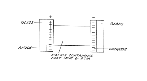
Figures 3 through 5 schematically illustrate
the electrochromic device of the invention. Figure 4
illustrates the matrix material with no electric field
present and Figure 5 illustrates the matrix material with
an electric field present. The electrochromic device may
be fabricated to have anodic electrochromic properties or
cathodic electrochromic properties, as desired.
''''
'
~3~
g/10
Reference is now made to Figure 3. In this
preferred embodiment~ an anodic ECM is disclosed. A
first glass sheet has an anode thereon and a second glass
sheet has a cathode thereon. In both cases, in
accordance with the preferred embodiment of the
invention, thP glass sheets have a thickness of 1/8 inch
and the electrodes have a thickness of about 2000
angstroms. In accordance with the teachings of the
preferred embodiment, both the anode and the cathode are
formed from tin oxide doped with fluorine. Such a
coating may be applied to the glass sheet by a pyrolytic
process, as is well-known in the art. It is, of course,
apparent that other electrode materials may ~e used and
other materials may be substituted for the glass sheets,
for example, quartz, plastic, etc. Generally, one, or
both, of the electrode supports should be transparent so
that the colors developed in the electrochromic material
may be viewed.
~ 1
~L3~
-- 11 ~
As shown in Figure 3 in the preferred
embodiment, a matri~ material is provided that supports
therein both finely divided ion producing material and
finely divided electrochromic material between the
cathode and the anode. Three examples of the preparation
of the matrix material supporting therein both finely
divided ion producing material and finely divided
electrochromic material will be set forth below.
Example 1.
The matrix material was prepared by dissolving
fifteen percent (15%~ by weight poly~inylbutyral powder
(B-90) with eighty five percent ~85%) by weight of a
methanol acetone mi~ture to form a solution. ~ormally
the powder forms from ten percent (10%) to twenty percent
(20%) by weight of the solution. The polyvinylbutyral
powder was purchased from Monsanto Company as B-90
- powder. The gelled polyvinylbutyral is an ionic
conductor but not an electronic conductor. The acetone
methanol mi~ture was five percent (5%) by volume acetone.
A finely divided ion producing material was
added to the solution. The preferred ion producing
material was lithium chloride (LiCl). This material was
added to the solution in an amount of 0.5% by weight of
the solution. The ion producing material may be added up
to the point that it saturates the solution. Other ion
producing materials include NaCl, KCl, LiBr, LiI, NaBr,
KBr, LiF, NaF, KF, cryolite, as w~ll as strong bases such
as NaOH and KOH. PlacPment of the ion producing
materials in the solution improves the ionic conduction
of the material produced by the solution.
A finely divided electrochromic material is also
added the the solution. In this Example the material
added is electrochromic lead oxide. The amount of lead
oxide added to the solution is the amount of lead oxide
:
.
'
~3~
- 12 -
it would required to produce a layer having a thickness
of 4000 A on one of the electrodes. A range of lead
o~ide additions would be sufficient lead 02ide to produce
a layer having a thickness in a range from 3000 A to
5000 A. The electrochromic lead oxide is a cathodic
electrochromic material.
The solution so formed is then thoroughly
mixed. The solution polymexizes and condenses while
being stirred at room temperature to produce a gelled
matrix material supporting therein the finely divided ion
producing material and the finely divided electrochromic
material in fixed but generally distributed positions.
The gelled matri2 material supporting therein
the finely divided ion produciny material and the finely
divided electrochromic material in fized but generally
distributed positions is then positioned between the two
electrodes as is shown in Figure 3. The matrix material
has a thickness which depends on the type of material
used and the type of materials added thereto. In the
preferred case, the matrix has a thickness of about
O.lmm. Since electrochromic lead oxide is a cathodic
material, when a negative five volts was applied between
the anode and thb cathode, a grey color resulted in the
electrochromic device.
The production of the grey color may be
e~plained by aid of Figures 4 and 5. Figure 4 shows a
schematic illustration of the matrix containing the
finely divided ion producing material ~LI) and the finely
divided electrochromic material in a condition where no
voltage is applied to the anode and the cathode of the
electrochromic device of Figure 3. In this case the
electrochromic particles do not have a charge associated
therewith and the ions, both positive and negative, are
randomly positioned.
When the volta~e is applied to the
- 13 --
electrochromic device as described above, then the
electrochromic particles do have a charge associated
therewith as shown in Figure 5 by the plus and minus
signs on the polarized electrochromic particles. When
this charging occurs, positive light ions are drawn to
the negative end of the electrochromic particles and
nPgative light ions are drawn to the positive end of the
electrochromic particles. This action causes a reduction
of the negatively charged side of the electrochromic lead
oxide and results in the production of the grey color.
Example 2.
The procedure of Example 1 is followed except
that the solvent used to form the solution was five
percent (5%~ by volume isopropanol and ninety five
percent (95%) by volume methanol. The electrochromic
material used was electrochromic bismuth oxide.
Electrochromic bismuth oxide is a cathodic electrochromic
material. Thus when it is formed into an electrochromic
device such as shown in Figure 3, it will take on a grey
color when a negative two volts is applied between the
anode a~d the cathode of the device.
Example 3.
The procedure of Example 1 is followed except
that the solvent used to form the solution was
dipropylene glycol methyl ether (DPM~. The
electrochromic material used was electrochromic iridium
oxide. Electrochromic iridium oxide is an anodic
electrochromic material. Thus when it is formed into an
electrochromic device such as shown in Figure 3, it will
take on a blue black color when a positive two volts is
applied between the anode and the cathode of the device.
* * *
While the E~amples above show the use of either
~3~
1~ --
anodic or cathodic electrochromic particles embedded in
the matri~, it is possible to embed both types of
particles in the matri~ at the same time. If this is
done~ it is preferred that the two types of particles
have about the same switching times between their
uncolored and colored states. Also, if just anodic or
cathodic particles are to be used, the particles may be
mixtures of various types of anodic or cathodic
materials. Again it is preferred that the various types
of particles have about the same switching times between
their uncolored and colored states.
While polyvinylbutyral was used in the E~amples
as the major material for forming the gelled matri~
material, other similar materials may be used. For
example materials such as polyvinylacetate,
polymetharcylates, urethanes, acrylics, etc. which may be
used.
While particular embodiments of the invention
have been illustrated and described, it will be obvious
to those skilled in the art that various chang2s and
modifications may be made without departing from the
invention, and it is intended to cover in the-appended
claims all such modifications and equivalents as fall
within the true spirit and scope of this invention.