Note: Descriptions are shown in the official language in which they were submitted.
~L3~)4~1~8
-- 1 --
SILICON ELECTROLUMINESCENT DEVICE
This invention relates to a silicon electroluminescent device.
05 Silicon electroluminescent devices are required for the emerging field of integrated
circuits incorporating integrated optical, electronic and electro-optical components.
In IEEE Journal of Quantum Electronics, Vol QE-22, No 6, June 1986, Soref
and Loren~o describe silicon waveguides and electro-optical switches suitable for
incorporation in conventional silicon integrated circuits. Silicon waveguides in10 particular are suitable for transmission of the fibre-optic communications
wavelength interval 1.3-1.55 ~m. The field of silicon integrated optics does
however ]ack one important component; an electroluminescent light source in the
1.3-1.55 ~m wavelength interval suitable for integration in silicon.
15 Electroluminescence relates to the production of light (luminescence) by a medium
in response to passage of an electric current through the medium. A GaAs
semiconductor light emitting diode (LED) is a common form of electroluminescent
; device. Such a diode has a pn junction which is forward biased in operation.
Minority carriers are injected by the junction into regions of the diode where
20 recombination takes place giving rise to luminescence. This process is not the
~', only recombination route, and its efficiency may be expressed in terms of the
nurnber of photons produced per injected carrier (normally much less than unity).
Moreover, photons may be reabsorbed in the device after they are produced.
Accordingly, the process may be characterised by internal and external quantum
25 efficiencies. Of these the former is the number of photons produced per
injected carrier and the latter the number externally detected per injected carrier.
The latter is necessarily of lower magnitude. It can be very much lower, since
diode electrode and junction geometry requirements tend to conflict with those of
photon output. In the related field of photoluminescence, in which a light beam
30 is used to create free carriers for recombination, similar quantum e}ficiencies are
defined. However, their values tend to differ less because no junction or
electrode structure is required.
',
3 5
'; ''
~ ~1
~3~g8~
Group I]l-V LEDs such as GaAs or InGaAsP devices are highly efficient and
well developed; they exhibit internal quantum efficiencies of between 0.2 and
0.05. However, not being silicon-based, they cannot be easily integrated in
silicon.
05
Silicon-based electroluminescent devices have been described in the prior art
which produce luminescence from the following processes:
(I ) band to band transitions,
(2) transitions arising from rare earth metal dopants in silicon, and
(3~ recombination associated with irradiation-induced defect centres in
silicon.
Electroluminescence arising from band to band transitions in pn junction silicondiodes is described by Haynes et al, Phys Rev 101, pp 1676-8 (1956), and by
Michaels et al, Phys Stat Sol 369 p311 (1969). However, the internal quantum
efficiency is in the region of 10-5, four orders of magnitude lower than
conventional LEDs. It is a consequence of the indirect nature of the bandgap in
silicon, which is a fundamental problem.
A silicon LED incorporating a rare earth dopant is disclosed by Ennen et al,
Appl Phys Lett 46(4), 15 February 1985, pp 381-3. This device consisted of
epitaxially grown n and p ty,oe silicon layers doped with erbium. The Er dopant
was introduced by implantation providing an ion concentration of 5 .6 x 1 o18
25 cm-3. The diode exhibited an external quantum efficiency of 5 x 10⁻⁴, which
the authors o~erved was not of the order acceptable for device applications. It
is about two orders of magnitude below that of conventional LEDs.
Furthermore, rare earth ion implantation is disadvantageous for integrated circuit
applications, since it is not electrically inactive; ~ie it introduces unwanted energy
30 levels into the semiconductor forbidden gap. These levels tend to disrupt theelectrical properties of the host silicon. ln this connection, the Ennen et al
~; ~ device exhibits poor rectifying characteristics. Carrier injection, quantum
efficiency and luminescence are therefore poor. Rare earth dopants are also
unlikely to be compatible ~vith integrated circuit technology, since their use to
35 make integrated LEDs may disrupt neighbouring electronic devices on the same
:, :
` - 2 -
~: :
;~
~:
, .
~3~ 4~38
-- 3 --
silicon chip.
Silicon electroluminescent diodes incorporating irradiation generated defect centres
are disclosed by Ivan~v et al, Sov Phys Sol State Vol 6, No 12, pp 2965-6,
05 June 1965, and also by Yukhnevich, Sov Phys Sol State ~ol 7, No 1,
pp 259--260, July 1965. In both cases, luminescent defect centres were produced
by irradiation from a cobalt~O source with the Y-ray energies in excess of
1 MeV. Quantum efficiencies are not quoted by these authors, but it is well
known that irradiation at such high energy se~erely degrades diode electrical
properties. See for example "Radiation Effects in Semiconductors and
Semiconductor Apparatus", puhlished by the Consultants Bureau, New York. A
diode without significant radiation damage exhibits sharply increasing bias current
as a function of forward bias voltage until a saturation current is reached.
Radiation damage reduces both the rate of increase of forward bias current and
the saturation current. This reduction or degradation worsens with increasing
irradiating beam energy and dose. It is associated with worsening carrier
transport properties of the diode junction, with consequent reduction in internal
quantum efficiency. This indicates that irradiation dosage and beam energy
should be minimised in this form of diode, in order to minimise damage and
2û preserve the carrier injection properties of the rectifying junction. However, to
increase luminescence output, it is necessary to increase radiation damage. Thishas been demonstrated in the related field of photoluminescence by Davies et al,Sol State Cornmun Vol 50, plO57 (1984). The requirement for high luminescent
output consequently conflicts with that for efficient minority carrier injection, and
the conflict is not reconciled in the prior art.
It is an object of this invention ~o provide an electroluminescent device of silicon
material.
The present invention provides an electroluminescent device including a
luminescent region of silicon material and rectifying means for injecting minority
carriers into the luminescent region, and wherein the luminescent region contains:
,, ~.
,
~3~
-- 4 --
(i) at least 1 o16 carbon atoms cm~3 in solid solution arranged to trap
silicon interstitials and provide an irradiation generated luminescent defect
ceDtre concentration of at least 1014 cm-3,
(ii) a divacancy concentration less than 1015 cm~3, and
05 (iii) a dopant which is at least substan~ially electrically inactive and has
vacancy trapping properties and a concentration of at least 1016 cm~3.
The invention provides an electroluminescent silicon device based on irradiationactivated defect centres in which the cor flicting demands of minority carrier
injection and luminescence output are reconciled. In one embodiment, the
invention has been sho~vn to produce a one thousandfold improvement in
luminescence output intensity as compared to band to band recombination
radiation from a similar device. The above limits to the carbon, divacancy and
electrically inactive dopant concentrations are the extreme limits; in a preferred
lS embodiment the carbon, de~ect centre and electrically inactive dopant
concentrations are at least 1018 cm~3, 1016 cm~3 and 1018 cm~3 respectively.
Of these the first is above the maximum solubility lirmit of carbon in silicon.
The irradiation activated defect centres are preferably G centres, ie Cs-SiI~s
complexes which emit radiation in the 1.3-1.6 ~un band (Cs = substitutional
carbon, SiI ~ silicon interstitial). P or H centres may alternatively be employed.
The electrically inactive dopant may be oxygen, but preferably it is an element
; which is isovalent with silicon, ie Ge, Sn or Pb.
~5 In a preferred em~odiment, the rectifying means is a pn junction between the
hJminescent region and a second region of opposite conductivity type.
Alternathely, the rectifying properties of the diode may be obtained by
constructing it in Scho~tky barrier form.
~: ;
30 In an alternative aspect, the invention provides a method of manufacture of an
electroluminescent device, the method including the steps of:
-- 4 --
,_ . . _ __ ,_ _ . . _. _ . _ . _ _ _,, ... ,., ,_._ . , _.__ _ __ _ ,_,,_"___ _. _ _ _ . .. . ____ ____ .. . . _ .__ .. ..
. _ ._
''
' ~ .
.. ': ',
,
- s -
(i) forming a diode including a carbon-doped silicon electroluminescent
region containing vacancy trapping means, and
(ii) irradiating the luminescent region with an electron beam having
energy sufficient to produce vacancies but insufficient for direct creation of
05 divacancies.
Despite the teachings of the prior art thae irradiation to produce luminescent
defect centres degrades diode properties unacceptably, it has surprisingly proved
possible to manufacture a diode which combines acceptable luminescence and
10 carrier injection characteristics. This has been achieved by irradiating at
moderate energies to create luminescent defect centres incorporating silicon
interstitials without generating significant numbers of divacancies which degrade
electrical properties. Furthermore, the use of vacancy trapping means inhibits
fonnation of divacancies arising from mobile single vacancies combining together.
The method of the invention preferably involves formation of the diode
luminescent region with a carbon dopant concentration of at least 1018 cm-3,
this being above the maximum solubility limit for carbon in silicon5. Vacancy
trapping is preferably provided by doping the luminescent region vith Ge, Sn or
20 Pb, although an oxygen dopan~ may also be employed. The electron beam
; ~ energy and dosage may be in the ranges 150 keV to 400 keV and 1015 to 1019
electrons cm~2 respe~tively, where higher be~m energy corresponds to lower
dosage. Preferably however these ranges are 290 keV to 310 keV and 1016-1018
electrons cm-2.
~5
The invention also provides an electroluminescent device made by the foregoing
method.
In order that the invention might be more fully understood, embodiments thereof
30 will now be described by way of example only, with reference to the
accompanying drawings wherein comrnon parts are like-referenced, and in which:
. ,
5 _
~ `"' '' ' ' ' '
~ "
, ' ~
: L3~4~
-- 6 --
Fîgure 1 shows an edge-emitting light emitting diode of the invention in a
cryostat with a part removed to facilitate viewing of interior detail;
Figures 2 to 6 illustrate steps in the manufacture of the Figure 1 diode;
Figure 7 shows a 4.2K photoluminescence spectrum from a diode structure of
05 Figure 3 which has been electron irradiated without the aluminium
deposition step of Figure 4;
Figure 8 shows a 77K photoluminescence spectrum from the diode structure
used to obtain the Figure 7 spectrum;
Figure 9 shows two 77K electroluminescence spectra, one from the Figure 1
diode, and the other from an unirradiated diode manufactured in
accordance with Figures 2 to 4 and 6 (ie an irradiated and
unirradiated diode respectively);
Figure 10 sho~s two superimposed l-V curves at 293K for the diodes used to
produce the spectra of Figure 9;
15 Figures 11 to 13 illustrate the radiation damage proces~ses which occur within
irradiated carbon doped silicon;
Figure 14 shows a summary of the Figures 1 I to 13 processes;
Figure 15 shows a graph of G-line photoluminescence intensity experimentally
obtained from a series of samples, and a theoretical
electroluminescent intensity as a function of energy of the irradiating
electron beam used in sample manufacture;
Figure 16 shows a light emitting device integrated into a CMOS microcircuit
substrate;
Figures 17 to 23 illustrate steps in the manufacture of the Figure 16 diode; and25 Figure 24 shows a light emitting device integrated into a CMOS microcircuit
: substrate with an integrated waveguide section for transmission of
light.
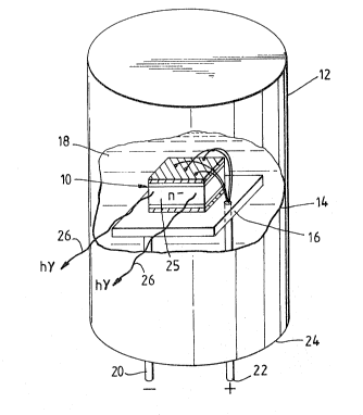
Referring to Figure 1, there is shown a light emitting diode 10 of the invention.
30 The diode 10 is incorporated in a cryostat 12 shown partly cut-away at 14.
Diode 10 is mounted on a metallic header 16, and immersed in liquid nitrogen
18 at a temperature of 77K. Connection leads 20 and 22 to the diode 10 are
fed through a base 24 of the housing 12, for external bias voltage supply. Lead
20 is connected to hçader 16 which in turn is connected to the lower face of
35 diode 10. Lead 22 is insulated from header 16 and is connected to the top face
. ~
'; ' ' , ~' :, ' `
~:
` :
.
~3~?49~8
of diode 10.
In operation, infrared photons as indicated by arrows 26 are emitted from an
edge 25 of the diode 10 when a voltage is applied across the leads 20 and 22
05 such that diode 10 is forward biased. The expression "edge" is conventionalterminology in the art of light emitting diodes. It relates to light emission inthe plane of an electroluminescent layer as opposed to perpendicular to it. As
illustrated however, Hedge" 25 relates to part of a diode face. The cryostat 12
has an infrared radiation transparent window (not shown) opposite edge 25 for
transmission of photons.
Figures 2 to 6 illustrate successive steps in the fabrication of the diode 10. Ahighly carbon doped silicon wafer 32 is prepared frorn a dislocation-free silicon
crystal with a substitutional carbon atom concentration of 2 x l o18 atom cm~3,
an interstitial oxygen concentration of I x 1 ol 8 atom cm ~3, and a phosphorus
dopant concentration of S x 101 5 atom cm~3. The wafer 32 is 200 llm in
thickness.
The concentration of substitutional carbon in the silicon wafer 32 is nearly an
order of magnitude above the norrnally accepted value for the rnaximum
equilibrium solubility limit for carbon in pure silicon (3 x 101 7 cm ~3). This is
` ~ achieved by pulling the silicon crystal vertically frorn a carbon doped melt within
a vertical magnetic field of between 1000 and 2000 gauss in strength. Under
these conditions it is possible to increase the oxygen content of the melt and also
to reduce carbon evaporation. High interstitial oxygen content stabilises the high
Ievels of carbon in silicon substitutional sites, as will be described later.
'
The~ upper surface 34 of the wafer 32 is polished and the iower surface 36 is
lapped. The upper wafer surface 34 is boron implanted with an ion dose of
5 x 10¹⁵ atoms cm~2 using ion energies of S0 keV. A simiiar phosphorus
:~ ~ implant on the lower surface 36 is carried out with an ion dose of 5 x I ol S
atoms cm~2 aDd ion energies of 100 keV. Activation af the boron and
phosphorus implants and removal of lattice damage are carried out by rapid
therrnal annealing at 1200 C for 10 seconds in argon. As shown in Figure 3,
this provides a heavily doped p-type or p+ layer 42. Consequently, a p~/n~
- 7 -
~3~48~
junction 43 is formed below the surface 34 at a depth of approximately 0.4 ~m.
Immediately above the surface 36, a heavily doped n-type or n~ contact 44 is
formed by the phosphorus implant.
OS As shown in Figure 4, the layers 42 and 44 receive respective metallisation layers
52 and 54, these comprising evaporated aluminium I ~Im in thickness. The
metallisation is fired at 450 C for 10 minutes in sintering gas to provide good
ohmic contacts to the layers 42 and 44.
The wafer 32 is irradiated with an electron beam as indicated by an arrow 60,
through the top surface 56 of the layer 52. The electron beam 60 has an
energy of 300 keV and a current density of 5 ,~Amp cm~2, and produces an
incident flux of 3.5 x I o16 electrons cm~2 on surface 56. The irradiation is
performed at room temperature with the wafer 32 supported on a heat sink.
The silicon wafer 32, and the aluminium layers 52 and 54, are scribed and
cleaved into areas of I mm2 to form 2 x 0.5 mm rectangular diodes such as the
diode 10. A lGwer surface 64 of the aluminium layer 54 is bonded to the
metallic header 16 with low temperature Epo-tek (Registered Trademark) H20E
conducting epoxy resin by curing at 80 C for 90 minutes. This provides
electrical connection of diode 10 ~o header 16. Four gold wires 62 each of
25 ~an thickness are thermocompression-bonded for electrical connection to
various points spread over the surface 56. This multiple connection to the
surface 56 distributes the input current and prevents the bonds from heating and2 5 becoming disconnected . The gold wires 62 are soldered to a terminus 66 of the
; ~ ]ead 22, which passes through and is insulated from the header 16. In addition,
lead 20 is connected to the header 16.
Referring to Figures 7 and 8, ~here are shown photoluminescence spectra 70 and
76 measured at respective temperatures 4.2K and 77K for diode structures formed
as described above but without the aluminium layers. The 4.2K
photolurninescence spectrum 70 vr.ls obtained ~vith 0.5 mW of argon ion laser
radiation at a ~vavelength of 5145 A. The 77K photoluminescence spectrum 76
~as obtained at the same excitation wavelength but a higher power of 100 mW.
The photoluminescence spectrum 70 of Figure 7 shows a zero phonon line 72
.
~3~L4~361
with a wavelength of 1.28 ~n and a vibronic sideband 74 between approximately
1.3 and 1.6 ~m. Both the zero phonon line 72 and the vibronic sideband 74
arise from a single type of defect known as a G-centre. The zero phonon line
arising from G~entres is knoY~n as the G-line. The photoluminescence spectrum
05 76 of Figure 8 also shows a G-line 78 and its vibronic sideband 80. In bothFigures 7 and 8 photon output arises from optical excitation of G-centres created
in the diode by electron beam irradiation.
The luminescence intensity of the G-line 78 is lower than the luminescence
intensity of the G-line 72. The relative intensity of the vibronic sideband 80
cornpared with its G-line 78 is greater than the relative intensity of the vibronic
sideband 74 compared with its G-line 72. However, above 77K the total
luminescence intensity of the vibronic band decreases with temperature.
The vibronic sidebands 74 and 80 extend throughout the 1.3-1.6 ~m wavelength
range, the spectral range of interest for optical communication. As will be
illustrated by subsequent data, G-centres show sufficient luminescence for VI~;I` interconnection purposes ~vhilst not greatly affecting the electrical properties of
the host silicon.
The photoluminescence spectra of the diode structures previously described are
~: generated by photons with an energy above the band gap, which inject minority
carriers into the silicon. Injection may alternatively be obtained by forward
biasing thç diode junction, which produces an electroluminescence spectrum as
previously mentioned. This displays features similar to the photoluminescence
spectrum of the diode, but is more sensitive to irradiation.
Referring now to Figure 9 there are shown two electroluminescence spectra 82
and 84 measured at a temperature of 77K. The spectra 82 and 84 were
obtained respectively from the diode 10 and from an otherwise equivalent diode
manufactured without the Figure S electron irradiation step. Spectn~m 84 is
.~ ~; plOned with a vertical scale 20 times larger than that of spectrum 82. Both
spectra correspond to diodes operated under forward bias with a junction currentdensity of 10 A crn~2. Photon output from diode 10 (spectrum 82) is due to
luminescence from the G-centres on the n~ side of the p l/n~ junction 43. The
g _
: ~
~3~8~
-- 10 --
electroluminescence spectrum 82 shows a G-line 85 and a vibronic sideband 86,
and the spectrum 84 shows contributions 88 and 89 due to band-to-band
recombination and olher processes respectively. A comparison of the two spectra
82 and 84 shows that the intçgrated intensity of the G centre electroluminescence
05 85 and 86 is approximately 1000 times greater than the integrated intensity of
the band-to-band electroluminescence 88 from the unirradiated diode. The
es~ternal quantum efficiency of the irradiated diode 10 is therefore 3 orders ofmagnitude higher than that of band-to-band transitions in an unirradiated but
otherwise equiva]ent diode. In the prior art of Ivanov et al, equal efficiencieswere obtained for luminescence from defect centres and band-to-band transitions.
Irradiated diodes suffer damage to their electrical properties. A measure of this
damage may be obtained from the current- voltage characteristic curves for the
diodes before and after irradiation as described by Vavilov et al in Radiation
Effects on Semiconductors and Semiconductor Apparatus previously mentioned.
At a chosen forward bias current, the bias voltages before and after irradiationare obtained from the respective current-voltage characteristic curves of a
particular diode. A ratio of these voltages indicates the degree of radiation
damage, and this ratio is defined as a radiation damage coefficient for the
2 0 purposes of this specification . A value of 2 for this coefficient signifies a typical
limit above Y~hich the diode performance becomes seriously impaired by
irradiation. Referring now to Figure 10~ there is shown an I-V characteristic 90,
having curves 92 and 94, obtained from irsadiated diode 10, and the unirradiatedequivalent diode, respectively. The radiation damage coeMcient for diode 10
obtained from cunres 92 and 94 is approximately 1.3. Accordingly, the rectifyingproperties of the diode 10 were not seriously impaired by the comparatively
modest irradiation treatment it underwent. It therefore combines good
lurninescence and carrier injection properties, unlike the prior art.
3 0 The invention provides luminescence arising from G-cen~res formed v~ithin the
diode 10 by irradiation. Each G centre is a compiex of two substitutional
carbon atoms and an interstitial silicon atom. Before the G~entres can be
formed by irradiation with silicon, the silicon should ideally be uniformly doped
with carbon on lattice sites. In practice, it is suMcient that the carbon be in
solid solution within the silicon, wherein a substantial proportion of the carbon is
-- 1 0
.~
., ~ .
~3~?~4~8
located on lattice sites. This may be achieved by incorporating the carbon
doping at the silicon gro vth stage as previously described, or by ion implantation
as vill be described later.
05 Referring to Figures 11 to 13, there are sho vn schematically examp1es of theinternal processes occurring vithin a silicon lattice 9S under electron irradiation.
The lattice 95 comprises silicon atoms, indicated by cross-hatched circles, and
carbon atoms, indicated by solid circles. The carbon concentration depicted by
Figures 1 I to 13 does not have any relation to the actual carbon concentration
10 of diode 10. In addition, the carbon atoms in Figure 11 to 13 are closer thanin a silicon sample and carbon doped as described earlier. On irradiation, as
shown in Figure 11, an electron 96 displaces a silicon atom 97, creating a
vacancy 98. The displaced silicon atom 97 then proceeds to displace a carbon
atom 99. Two further electrons 100 and 102 displace respective silicon atoms
15 104 and 106, forming respective vacancies 108 and 110. These vacancies may
migrate through the lattice 9S by movement of silicon and carbon atoms. In
Figure 12, they are sho~vn having migrated to neighbouring lattice sites to ~orm a
divacancy 112. This drawing also shows a carbon atom 114, freed by collision
with an electron displaced silicon atom, having displaced a silicon atom 116 and20 about to occupy its vacated lattice site; ie the silicon atom 116 becomes
substituted by the carbon atom 114. Figure 13 shows the silicon atom 116
having become trapped on an interstitial site. It is bound to the substitutional; ~ carbon atoms 114 and 118 to form a G-centre 120.
; ~ 25 Referring now to Figure 14, there is shown a schematic summary of the
processes occurring wtthin the lattice 95 upon irradiation. An electron 12~ may
directly create a vacancy 124 or if its energy is above the threshold for
divacancy formation, a divacancy 126. The electron 122 may also indirectly
create a G-cent. e 128 . A divacancy 130 may also be formed by two vacancies
30 132 and 134 which migrate together. ln the absçnce of other processes, the
vacancy 124 may anneal out at room~ temperature or contribute to a divacancy.
Divacancies and C;-centres do no~ anneal out at room temperature. Furthermore,
it is not possible to anneal out the divacancies vithou~ also annealing out
~-centres.
~: :
.
,
~3~?~4~
~ 12 --
As previously mentioned, irradiation of a diode impairs its rectifying properties,
which limits its possible electroluminescence. This damage is caused by the
divacancies created by irradiation. As the energy of irradiation rises, defects may
be created comprising three or more vacancies. However, in general the
05 concentration of these is small compared with the divacancy concentration, and
may be ignored. Vacancies may also cause damage to diode rectifying properties,
but these may be removed by vacancy traps as described later.
In this invention, it has been found that by restricting the concentration of
10 divacancies to below 1 û15 cm~3 the damage to the rectifying properties of anelectroluminescent diode can be kept to an acceptable level. In one embodirnent
of diode 10, the concentration of di~acancies was measured to be 2 x 10¹³
cm~3
15 Referring once more to Figure 14 there are at least two conditions which must be fulfilled to restrict the concentration of divacancies. These are:
(a) irradiating with an electron energy below the divacancy threshold
eDergy;
(b) preventing the combination of vacancies to form divacancies.
\
In the prior art, the divacancy threshold energy was not known. It ~as
estimated for the purposes of the present invention as ~ill be described later. It
was found that using irradiation energies of between 150 keV and 400 keV,
unacceptable concentrations of divacancies could be avoided. .
Prevention of divacancy formation by vacancy migration is achieved in this
invention by doping the luminescent region of diode 10 with oxygen. Apart
from stabilising the carbon content by relieving lattice strain, oxygen provides a
30 trap for vacancies. By arranging for the oxygen concentration to be above 1 o16
cm~3 (comparable with the carbon concentration), vacancies formed by irradiationare largely trapped before they may combine. In this way divacancy formation
by indirect processes is reduced to acceptable levels. Interstitial oxygen is largely
e]ectrically inactive dopant in that it does not introduce unwanted energy leYels
35 into the semiconductor to any substantial extent. In fact, interstitia] oxygen has
~ 12 -
.
~ ~ ,
' "
.. ~
13~ 38
-- 13 --
an electrical activity typically 1 o-2-10~ times that of a donor impurity, such as
phosphorus. Isovalent dopants such as Ge, Sn or Pb also provide vacancy traps
with even lower electrical activity.
05 As well as increasing dalnage to the diode's electrical properties, an increase in
the energy of electron irradiation dose increases the concentration of G-centresand hence also the internal quantum efficiency. The increase in damage and
G-centre concentration are competing factors, and no compromise between the
two to provide an emcient electroluminescent device has been achieved in the
prior art. In the following experiment, G-centre creation and concentration as afunction of electron irradiation energy are investigated by photoluminescence.
From the experimental results the damage to the rectifying properties of an
irradiated diode may be ascertained, as well as the vacancy and divacancy
creation threshold energies.
G~entre formation and corresponding luminescence emission were determined
using Czochralski-grown silicon samples. The carbon and oxygen concentration
differed between different samples by no more than 5%. The concentrations
were 6.1 x 1017 cm~3 and 1.0 x 1017 cm~3 respectively. Each silicon sample
was electron beam irradiated with a respective electron beam energy over the
range 120-400 keV, but the total energy deposited per unit area ~as kept
constant at 1.0 x 10¹⁹ keV cm~2. A respec~ive photoluminescence spectrum was
obtained for each silicon sample.
,~
Referring to Figure 15, there is shown a graph 150 of resulting G-line
photoluminescence intensity per unit irradiated area (arbitrary units) against
electron beam energy (keV) and beam dose (101 6 e~ cm~2), using data obtained
by experiment. A curve 152 illustrates the intensity of G-line luminesceDce
emanating from a unit irradiated area as a function of electron beam energy.
; ~ 30 Curve 152 exhibits a threshold value for G-centre~ creation of 1S0 keV. It is
considered that this value corresponds to a threshold value for silicon interstitial
creation by collisional displacement.
3_
. : , , : .
:
~L3~4t~E~
-- 14 --
Above 150 keV on graph 150, the curve lS2 rises rapidly. This demonstrates
that between 150 keY and 300 keV, the creation of G-centres is strongly energy
dependent; it varies by an order of magnitude between 225 keV and 300 keV.
The curve 152 has a knee 154 above which it can be seen that little increase is
05 gained in G-line intensity for further increase in the electron beam energy.
Below the knee 154, G-line intensity drops rapidly.
As previously mentioned, the internal quantum efficiency of photoluminescence
from irradiated silicon is not as dependent on irradiation damage as that of
10 electroluminescence. As a result, photoluminescent emciency is not as sensitive
to irradiating beas~ energy as electroluminescent efficiency. The knee 154 on
graph 152 indicates thaS photoluminescence is beginning to be affected by
divacancy formation. Although G~entre concentration increases above the knee
154, the for~nation of divacancies also provides non-radiative recombination
15 centres which reduce the number of carriers available for radiative recombination
at G~entres. Divacancies also impair the rectifying properties of diodes forrnedby irradiation at energies above the knee 154. Consequently, beam energy
affects electroluminescence more seriously than photoluminescence. A theoreticalcurve 156 shows the expected beam energy dependence of electroluminescent
20 output from diodes incorporating respective silicon samples. Electroluminescence
decreases beyond the knee 154, indicating that the increase in G-centre creationhas become outweighed by availability of competing non-radiative processes.
Another experiment was used to determine the point at which electroluminescence
2S is significantly affected. In this experiment, further 200 ~m thick silicon samples
containing 2 x I o18 cm-3 ca}bon atoms were irradiated at electron energies
between 200 and 400 keV at a constant energy~dose product of 1.0 x 10¹⁹ keV
cm~2. Resistivity was measured for each sample before and after irradiation. In
a sample irradiated at 400 keV a change in resisitivity of 14% was observed.
30 Resistivity changes in samples irradiated at lower energies were insignificant. The
divacancy concentration of the 400 keV irradiaeed sample was measured to be S
x 1 o15 cm~3 . This corresponds to a significant reduction in electroluminescentinternal quantum efficiency. HoweYer, by maintaining the electron dose below
1016 electrons cm~2 the divacancy concentration can be maintained below 1015
35 cm~3 at 400 keV.
14
-- -- . . -- . _ . . . .. . . . . . . ... ... .... .. .. . ... . .. . .. . .. _
. . .
.
~L3~
- 1S -
Th~ previous experiments indicate that the vacancy creation threshold is
approximately 150 keV, and the divacancy creation threshold is above about 300
keV, and an unacceptable divacancy concentration is obtained abo~le 400 keV.
Electrolur~inescent devices arc manufactured in accordance with the invention with
05 irsadiation energies above Lhe vacancy creation threshold and belo~v beam energy
producing unacceptable divacancy concentrations. The range of acceptable
irradiation energies is 150 to 400 lceY. Beam energies in the region of the kneeIS4 produce the greatest lurninescence intensity consistent with acceptable
divacancy concentrations. Therefore, as in the manufacture of diode 10,
10 Yrradiation energies between 290 and 310 keV produce de~ices with expected
optirnum luminescent output.
The luminescent output of an irradiated diode is also dependent on G~entre
concentration. Below a ce~ain concentration, internal efficiency is below that of
15 band-to-band tsansitions. At a G-centre concentration below 1012 cm~3,
efficiency is unacceptably low irrespective of the divacancy content. Above thisG-centre concentration, the efflciency is dependent on divacancy concentration.
At a fixed irradiation energy, within the limits given above, the G-centre
concentration is dependent on the carbon concentration and the irradiation dose.20 Moreover, the maximum dosc is limited to that which does not severely impair
diode rectifying characteristics and internal quantum efficiency. An excessi~e dose
produces a significant concentration of shallow carrier traps, such as a
vacancy/oxygen atom comple~. At room temperature these traps are not
important because carrier mobility prevents effective trapping. However, at 77K,25 shallow traps become more effective and hence more signif~cant.
In addition to impairment of re tifying properties, increased dosage requires
increased processing time. This is commercially unattractive. It also causes
heating, which tends to anneal out G-centres and reduce luminescent efficiency.
30 The~e l~mits on the dose mean the carbon concentration must be greater than
1016 m~3
3S
-- 15 -- .
~b "~
.
~L3~44l3~
-- 16 --
To produce an acceptable electroluminescent device, using irradiating beam
energies in the range 150-400 keV, the range of practical doses varies dependingon the beam energy chosen. For an irradiating energy of 150 keV, the dose
may be between 1018 to 1019 electrons cm~2, and at 400 keV, between 1015 to
05 1016 electrons cm~2. At the preferred energy of about 300 keV, th~ dose range
is 1016 1018 electrons cm~2.
Each C;-centre is associated with two adjacent substitutional carbon atoms and an
interstitial silicon atom. .9ccordingly, a high carbon consentration results in a
high G-centre concentration upon irradiation. The diode 10 has a carbon
concentration above the maximum equilibrium solubility limit of carbon in pure
silicon. This carbon concentration is comparatively high, and enhances the
internal quantum efficiency of the diode 10. The aforementioned fabrication
steps achieve this concentration by pulling a silicon crystal vertically upwards from
a carbon-rich melt in a ver~ical magnetic field. In addition, under these
conditions, it is possible to increase the oxygen content of the melt and
consequently reduce carbon evaporation. In addition, high interstitial oxygen
content stabilises high levels of substitutional carbon. Further details are set out
by K G Barraclough et al in Proc Fifth Int Symposium on Silicon, Mat Sci and
Tech, "Silicon 1986", edited by Huff et al and published by the Electrochemical
Society.
Another metAod for producing high carbon concentrations in single crystal silicon
comprises low pressure vapour phase epitaxial grow~h or molecular beam epitaxy
at temperatures below 850 C. At low temperatures, the solid solution may be
maintained above the maximum equilibrium solubility limit due to carbon diffusion
and precipitation being kinetically hindered.
A third method for increasing the carbon content is by ion implantation, followed
by pulsed laser annealing in the melt regime or by rapid thermal annealing of
the solid phase.
9~3~
G-centres may be amphoteric in nature, which means they may act as both hole
and electron traps. Consequently, G-centres may be located on the p-side or
n-side of a p-n j~mction. In the diode 10 the G-centres are located on the n~
side of the p+ln~ junction 43. Additionally, the n~ side is doped with
05 phosphorus, which unlike boron does not compete with carbon for silicon
interstitials. Boron is the dopant for the p+ side, therefore the efficiency of the
device 10 would be affected by locating the G-centres on that side.
The invention is not restricted to devices utilising p-n junctions as rectifying10 means. PIN and Schottky structures may also be used to inject carriers into the
region containing G-centres.
Electroluminescence may also be achieved in silicon junction diodes containing
defect centres other than G~entres. Such luminescent centres include known
15 carbon-related defects which produce the H and P ~ero phonon lines at
wavelengths of 1.34 ~m and 1.61 ~n respectively. Other examples of carbon-
related, irradiation-generated defect centres are presented by G Davies et al in J
Phys C Solid State Phys IA99-503 (1984).
20 Furthermore, even higher levels of carbon may be shbilised in substitutional sites
by co-doping with isoelectronic group IV elements, namely germanium, tin or
lead. As indicated previously, the resulting increase in the concentration of
luminescent centres will further increase the diode efficiency.
25 The invention may be incorporated in integrated circuits. In this case it is
necessary to produce localised optical centres within a conventional material
structure. Thus rather than use a high carbon wafer as previously described, thetechnique of carbon ion implan~ation in combination with transient annealing, orselective area epitaxy, and near-threshold selective electron irradiation would be
30 used for creation of localised G-centres.
;. .
17
.
~3~ 4~
- 18 -
Referring now to Figure 16, ~here is schematically shovrn a light emitting diodedevice 200 having a form compatible with CMOS microcircuit construction. The
de~rice 200 consists of a heavily doped n-type or n+ silicon semiconductor
substrate 202 surrnounted by a lightly doped n-type or silicon semiconductor
05 epita~ial layer 204. A silicon oxide layer 206 covers the layer 204, except for a
wi~dow 20B above a carbon doped region 218 and a p+ semiconductor contact
210. 8elow the regio~ 210 is a p+/n~ junction 212. Aluminium layers 214 and
216 are deposited above th~ o~ide layer 206 and contact 208, and below the
substrate 202 respectively for electrical conaection purposes.
Referring ~ow to Fi~es 17 to 23, there are schematically shown the stages of
manufacture of tho device 200. The n+-type semiconductor substrate 202 is
formed from a C~ochralski gro~n dislocation-free silicon crystal and is
antimony-doped with a concentration of S ~ 1018 ator~s cm~3. The n~
semiconductor layer 204 on the ~ubstrate 202 is grown by known epitaxial
methods and phosphorus-doped wit& a concentration of S x 1015 atoms cm~3.
Layer 204 may be 5 to 10 pm in thickness. All doping is perforrned using
known techniques. The substrate 202 together with the layer 204 forrns a
comrnon starting element for p-well bulk CMOS microcircuits.
The silicon oxide layer 206 is produced by the stanclard process step of thennaloxidation, ant is typically O.S to 1 ~n thick. The window 208 in oxide layer
206 is produced by the known technique of wet etching and is typically a square
with 10 lun sides.
A carbo~oped region 218 of the layer 204 is produced below the window 208
by ion implantation using ion energies of 180 keV and a dose of a~ut
1014 atoms cm~2
The p+-type semiconductor contact 210 is produced by boron doping the
carbon~oped region 218 by ion implantation with low ion energies, ie 30 keV,
and a dose of typically S x 1015 atoms cm~2. This produces a boron-doped
region with an implant range of 0.1 ~n. The p~/n- junction 212 is formed at
a depth of 0.3 ,~lm below the windo~ 208. Boron and carbon doping create a
3S carbon-rich layer 220 within the deple~io~ layer of device 200, the layer being
-- 18 --
. .. ... .. . . ... . ... .. ... . . .. ... ... . . . .. . . ... . . . . .. . .. . . . .. .
.
-
~1.3~488
-- 19 --
on the n~ side of the p~/n~ junction 212. The dep]etion layer has a width of
approximately O.S ~un and extends below the carbon-rich layer 2~ 8.
Activation of the boron implant and production of a supersaturated layer of
05 carbon is achieved by rapid thermal annealing.
The con~acts 214 and 216 are formed on the upper p~ surface, and on the base
of the n+ substrate by Al or Al-Si{~u evaporation and low temperature alloying,
10 for example, 450 C for 10 minutes.
As previously described, G-centres are created in the carbon-rich layer 220 by
electron irradiation at electron energies in the range 150 keV to 400 keV with adose in the range l ol 6 ~o 1 ol 9 e~ cm~2. It is essential to avoid silicon lattice
15 damage aDd tsapping of charge in the oxide of neighbouring parts of the
microcircuit. Such damage may be avoided by focussing the electron beam on
the window 208. Moreover the beam may be scanned within the area of the
window.
20 Referring now to Figure 24, in which parts equivalent to those of Figure 23 are
like-referenced, there is sho~vn an alternative embodiment of the device 200
arranged to have optical waveguide properties. In this embodiment, the device
200 has a central region of increased thick~ness to accommodate a waveguide 224
within which active diode components are located. The waveguide 224 has
25 somewhat oblique wall construction as an artefact of production by wet
anisotropic etching. Photon output from the device 200 is guided to another part(not shown) of the layer 204 by the waveguide 224. î`his provides for optical
communication between different microcircuit regions. The waveguide 224
incorpora~es the n~-type layer 204 in the; region 220, and photons generated by
30 device 200 are vraveguide confined.
g_
`:~
'~
.
.