Note: Descriptions are shown in the official language in which they were submitted.
4~
The present invention relates to a three-dimensional
imaging apparatus for picking up an image of an object
stereoscopically.
Fig. 1 is a block diagram showing a schematic
configuration of a three-dimensional imaging apparatus
according to an embodiment of the present invention.
Fig. 2(a) is a diagram schematically showing a
configuration of an image pick-up device using a three-
dimensional imaging apparatus.
Figs. 2(b) is a timing chart for operation and switching
liquid crystal shutters.
Figs. 3(a) and 3(b) are timing charts for the operation
of an image pick-up device and switching of liquid crystal
shutters.
Figs. 4(a) and 4(b) are timing charts for the operation
using an image pick-up tube as a three-dimensional imaging
apparatus.
Fig. 5 is a block diagram of a conventional three-
dimensional imaging apparatus.
Fig. 6 is a block diagram showing optical shutters.
In a basic method conventionally known for imaging an
object three-dimensionally, an image of an object is picked
up by use of two television cameras held at a predetermined
angle to each other and GUtpUt signals of these two
~; 25 television cameras are switched alternately for each field.
~ ~ .
~;
~I!L3~
A configuration of such a three-dimensional imaging apparatus
is schematically illustrated in Fig. 5. In Fig. 5, the side
A delineated ~y one-dot chain shows a three-dimeneional
imaging apparatus and he side B a three-dimensional display
unit. In this drawing, reference numeral 1 designates an
object to be imaged, numeral 2 a television camera A, and
numeral 3 a television camera B. The television cameras A
and B have the lenses thereof arranged on the front of the
imaging surface thereof. Numeral 4 designates a sync signal
generator, numeral 5 a switch, and numeral 6 an adder, which
make up a three dimensional imaging apparatus. Numeral 7
designates a sync separator, numeral 8 a monitor television,
and numeral 9 a pair of spsctacles, which make up a three-
dimensional display unit.
The three-dimensional imaging apparatus and the three-
dimensional display unit configured as described above are
well known and there~ore will be explained hereinafter only
briefly. First, reference is had to the three-dimensional
imaging apparatus. The teleYision cameras 2 and 3 are
arranged at a given angle e to the
` ~ - 2 -
`' ' ,- .
~3Qg~
l same object l~ Also, the scanning timings of the tele-
vision cameras 2 and 3 are held in synchronous relation-
ship with each other. As a result, the television
cameras 2 and 3 are supplied with a pulse-like signal
at the same time as required for driving the television
cameras from the sync signal generator 4. (The TV cameras
2 and 3 correspond to the right and left eyes respectively
of the human being.) A video output signal of each of
the TV cameras 2 and 3 is connected to the terminals A
and B of the switch 5 respectively. The switch 5 is
controlled by a field pulse supplied from the sync signal
generator 4. At the terminal C of the s~7itch 5, there
are produced a video signal from the TV camera l in the
first field and a video signal from the TV camera 2 in
the second field as alternate output signals. A video
signal thus produced by being switched and a sync signal
from the sync signal generator 4 are applied to the adder
6 thereby to produce a three-dimensional video signal.
A drive pulse for the television cameras, a field
~` 20 pulse and a sync signal produced from the sync signal
generator 4 are of course in synchronism with each other.
Now, the three-dimensional display unit will
be explained. A thrae-dimensional video signal produced
from the above-mentioned three-dimensional imaging
apparatus is transmitted to a three-dimensional display
unit by predetermined means. The three-dimensional video
signal thus transmitted is supplied to and displayed on
the monitor television 8. The three-dimensional video
~3~ 3~
1 signal displayed on the monitor TV 8 is obtained from
the video output signals of the TV cameras 2 and 3
alternated with each other, and therefore is not felt as
a three-dimensional ima~e in its direct form but as an
unnatural double image.
If the image displayed on the monitor TV 8 is
to be watched as a three-dimensional image, the image
picked up by the TV camera 2 is observed only with the
right eye, and the image taken by the TV camera 3 with
the left eye of the viewer. Specifically, the images
displayed on the monitor T~ 8 are selected in such a manner
that the image in the first field enters the right eye
and the image in the second field enters the left eye.
As a means for accomplishing this purpose, the spectacles
9 having an optical shutter function are used to select
optical signals from the monitor TV 8 in such a way that
the image of the first field is observed by the right eye,
and the image of the second field by the left eye. The
sync separator 7 produces a field pulse synchronous with
the sync signal. The field pulse output signal from the
sync separator 7 is assumed to be at high level in the
first field and low level at the second field. The field
pulse is applied to the spectacles 9, so that the optical
shutters built in the spectacles 9 are turned on and off
alternately thereby to select the optical signal from the
monitor TV 8 for the right and left eyes. Specifically,
the optical shutter for the right eye of the spectacles 9
passes the light in the first field, while the light is
. ~
- 4 -
~.3~
1 masked by the optical shutter for the left eye. In
reverse, the optical shutter for the left eye of the
spectacles 9 passes the light in the second field, while
the light is mas~ed by the optical shutter for the right
eye. In this manner, the optical signal from the monitor
TV 8 is selected to observe a three-dimensional image.
Now, the optical shutters will be briefly
explained. Each optical shutter, which may be of mechanical
type, is used in the form of liquid crystal shutter in the
present embodiment. In the li~uid crystal shutter, inter-
ruptions of light is capable of being controlled by a
voltage, and the response speed is sufficiently high as
compared with the field scanning frequency of the TV
camera. It is also long in service life as compared with
the mechanical shutter and easier to handle.
A liquid crystal shutter will be briefly
described below with reference to Fig. 6 schematically
showing an image of an object. Numerals 10, 11 designate
deflection plates, numeral 12 a liquid crystal, numerals
13, 14 transparent electrodes, numeral 15 a rectangular
wave generator, numerals 16, 17 AND gates, numerals 20,
21 capacitors, numeral 18 an inverter, and numeral 19 a
field pulse input terminal. In a basic configuration
of an optical shutter, -two types of deflection plates 10,
11 have a liquid crystal (twist nematic type) 12 arranged
therebetween and the liquid crystal is impressed with an
electric field. In this way, an optical shutter is -
~ configured for interrupting light. The twist nematic
;~ - 5 -
~3C?~L9~
1 crystal is well known and will not be described any
further.
The optical section of the optical shutters
100, 200 is made up of deflection plates, a liquid
crystal and a transparent electrode. The deflection plate
10 passes only the horizontal polarized wave and the
deflection plate 11 only the vertical polarized wave of
the light from the object. The transparent electrode 14
is grounded. The transparent electrode 13 is used for
applying an electric field to the liquid crystal 12. In
this configuration, if no voltage is applied to the
transparent electrode 13, the horizontal polarized wave
that has passed through the deflection plate 10 also
passes through the liquid crystal layer 12 thereby to be
phase-shifted into a vertical polarized wave, and the
vertical polarized wave that has passed through the
liquid crystal layer 12 is transmitted through the
deflection plate 11. Specifically, the liquid crystal
shutter is thus transmittable, so that the light from the
monitor is capable of reaching the eyes of the human
being. If a voltage is applied ~o the transparent
electrode 13, on the other hand, the horizontal polarized
wave that has passed through the deflection plate 10 is
passed also through the liquid~crystal layer 12 but not
phase-shifted and maintains the horizontal polarized state
thereof. As a result, the horizontal polarized wave
that has passed through the liquid crystal layer 12 is
unable to pass through the deflection plate 11.
6 -
:
.~ :......
~L3~
1 Specifically, the liqujd crystal shutter is masked, and
therefore the light from the monitor is unable to reach
the eyes of the human being. As described above, the
transparent electrode 14 is grounded, and the transparent
electrode 13 is supplied with a drive signal through
capacitors 20, 21. The drive voltage applied to the
transparent electrode 13 is about 10 V with a drive
frequency of about 200 Hæ. This drive signal is produced
by the rectangular wave generator 15, the AND circuits 16,
17, the inverter 18 and the field pulse input terminal
19. Specifically, the rectangular wave generator 15
generates a rectangular wave of about 200 Hz, and this
output signal is applied to the AND circuits 16 and 17 at
the same time. The AND circuit 16 is supplied from the
field pulse input terminal 19 with a field pulse high
in level for the first field and low in level for the
second field. As a result, the output signal of the AND
circuit 16 provides a drive signal for the liquid crystal
; layer only for the first field. The AND circuit 17, on
the other hand~ is supplied from the field pulse input
terminal 19 with a field pulse inverted by the inverter
18, and therefore the output signal of the A~D circuit 17
makes up a drive voltage of the liquid crystal layer
only for the second field. A liquid crystal shutter is
thus constructed. Specifically, the shutter 100 on the
right side of the spectacles 9 passes the light for the
first field, and the shutter 200 on the left side of the
spectacles 9 allows to pass the light for the second field.
- 7 -
. . ~
The three~dimensional imaging apparatus having the
configuration described above, however, requires two TV
cameras and high in cost. It is also necessary to adjust
precisely the image angle, focal point and angle of an obj~ct
to the two TV cameras in picking up an image by the two
different TV cameras~ As a result, a long time is consumed
as compared with the actual time of imaging. Further, the
problem has been posed by the lack of mobility.
The present invention provides a three-dimensional
imaging apparatus having a low-cost configuration which is
easy to adjust. According to the present invention, there is
provided a three-dimensional imaye pickup apparatus having a
television camera provided with an imaging device which
comprises at least photoelectric converting elements and
vertical transfer stages corresponding to said photoelectric
converting elements, said imaging device reading out signal
charges stored in said photoelectric converting elements one
or more times in one field by transferring the signal charges
simultaneously to said vertical transfer stages, wherein
object images transmitted through two optical paths are
alternately selected for every field to be picked up,
substantially synchronous with the transfer timing of
transferring the signal charges from said photoelectric
converting elements to said vertical transfer stages~
`:~
~ 8 ~
r,~
~.3q~ ~¦`Y~ L~
1 In this confi,guration, object images from two
light path systems are selected alternately in synchronism
with the field scan of the imaging device thereby to pick
up a three-dimensional image with a single TV camera.
In the process, an image pick-up device used for the TV
camera includes at least a photo-electric transducer and
a vertical transfer means. In the case where the photo-
electxic transducer doubles as a vertical transfer means,
however, a signal charge storage section is provided along
the extension of transfer by the vertical transfer means,
so that signal charyes stored in each photo-electric
transducer element are transferred to corresponding
vertical transfer means substantially at the same time
thereby to pick up an image for a screen. For this
purpose, an image pick-up device capable of plane scan is
used. The storage time of signal charges at each photo-
electric transducer element of the image pick--up device
is not more than the scanning time of a field. The object
images from two light path systems entering the image
pick-up device are alternately switched for each field
by use of optical shutters at substantially the same
timing as signals charges are transferred from the photo-
electric transducer of the image pick-up device to the
vertical transfer means. By using this image pick-up
device, keeping the storage time of signal charges at
each photo-electric transducer element of the image pick-up
device at not more than the scanning period for a field,
and switching the optical path systems at substantially
g
.
,
~3~
the same timing as the signal charges are trallsferred from
the photo-electric transducer of the image pick-up device to
the vertical transfer means this way, it is possible to pick
up a three-dimensional image of high image quality with a
single TV camera.
A three-dimensional imaging apparatus according to an
embodiment of the present invention will be explained below
with reference to the accompanying drawings.
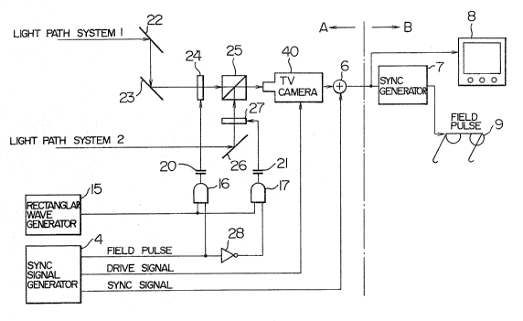
In Fig. 1, the side A designated by one-dot chain is a
three-dimensional imaging apparatus and the side B a three-
dimensional display unit. Reference numeral 40 designates a
TV camera, numeral 4 a sync signal generator, numeral 6 an
adder, numerals 22, 23, 26 mirrors, numerals 24, 27 liquid
crystal shutters, numeral 25 a half mirror, numeral 28 an
inverter, numerals 16, 17 AND circuits, numeral 15 a
rectangular wave generator~ numerals 20, 21 capacitors, and
numeral 100 a liquid crystal drive circuit. The mirrors 22,
23, the liquid crystal shutter 24 and the half mirror 25 make
up a first light path system, and the mirror 26, the liquid
~ 20 crystal shutter 27 and the half mirror 25 a second light path
:~ system. ~he sync signal generator 4, the adder 6, mirrors
22, 23, 26, the liquid crystal shutters 24, 27, hal~ mirror
25 and the TV camera 40 provide a three-dimensional imaging
apparatus.
`
~ 25
`~ - 10 -
:
1 Now, the operation of this configuration will
be explained. The TV camera 40 is supplied with a pulse-
like signal required for driving the TV camera from the
sync signal generator 4. ~lso, the drive pulse, the
field pulse and the sync signal for the TV camera produced
from the sync signal generator 4 are all in synchronism
with each other. The light entering from an ohject
through the mirrors 22, 23, and liquid crystal shutter
24 passes through the half mirror 25 and forms an image
at the photo-electric transducer section o~ the image
pick-up device of the TV camera 40. The light entering
from the object through the mirror 26 and the liquid
crystal shutter 27, on the other hand, is bent by 90
degree through the half mirror 25 and forms an image
at the photo-electric conversion section of the image
pick-up device of the TV camera 40. The optical axes of
the light path systems 1 and 2 are arranged at a given
angle ~ (not shown) against the same object. (The light
path systems 1 and 2 correspond to the right and left eyes
respectively of the man).
The optical shutter used for the present
invention is a liquid crystal shutter long in service
life, in which the light interruptions can be controlled
by a voltage and the response speed is sufficiently hi~h as
compared with the field scanning frequency of the TV camera.
This optical shutter using liquid crystal is substantially
of the same construction as the one described with
reference to Fig. ~. Since they are also the sa~.e in
.
.
1 operation and will be described only briefly.
The li~uid crystal shutters 24, 27 are comprised
of deflection plates 10, 11, liquid crystal 12 and
transparent electrodes 13, 14 shown in Fig. 6. The
liquid crystal shutters 24, 27 are controlled by the
drive pulse supplied from the liquid crystal shutter drive
circuit. As already explained with reference to Figs. 4
and 6, the liquid crystal shutters pass the light when
the field pulse supplied to the AND circuits 1~, 17 making
up the liquid crystal shutter drive circuit is at low
level. The field pulse is high in level for the first
field, and low in level for the second field. As a result,
the liquid crystal shutter 27 shown in Fig. 1 passes the
light for the first field, and the liquid crystal shutter
24 allows the light to pass for the second field. The
light signal representing an object image that has passed
the second light path system enters the image pick-up
device for the first field, and the light signal carrying
an object image that has passed the first light path
system enters the image pick-up device for the second
field.
The image pick-up device is basically adapted
to receive a light signal at the photo-electric transducer
section from an object image over the period of one field
or one frame, and after accumulating (storing~ ~he signal
charges over a period of one field or one frame upon
photo-electric conversion, reads out the signal charges
thus stored. Thereforel an output signal is delayed by
- 12 -
l one field behind the light signal entering the image
pick-up surface.
If an image pick-up device or image pick-up
tube of linear sequential scan type or an X-Y matrix
image pick-up device (MOS image pick-up device) is used
for the TV camera 40, it is impossible to obtain a three-
dimensional imaging signal for the reason explained below
with reference to Fig~ 4. Fig. 4(a) is a diagram
illustratively showing the scanning field of the TV camera
and the liquid crystal shutter conditions and the potential
at point A of the image pick-up surface (photo-electric
transducer section) of the image pick-up device of linear
se~uential scan type, and Fig. 4(b) a diagram showing
the image pick-up surface of an image pick-up device of
linear sequential scan type. A light signal enters an
image pick-up device after passing through a second light
path system (liquid crystal shutter 27) from an object
image in the first field, and after passing through a
first light path system (liquid crystal shutter 24) in
the second field. By way of explanation, the light
signal that has passed the first light path system is
called the light R, and the one that has passed the
second light path system the light L. Explanation will
also be made of a case in which an image pick-up device
of linear sequential scan type, that is, an image pick-up
tube, is used. The potential at point A of the image
pick-up surface of the image pick-up tube undergoes a
gradual change with time as shown in Fig. 4(a) by storage
- 13 -
~-3~
1 of signal charges, and at a predetermined timing, the
signal charges at point A are read out. The signal
charges generated at point A, however, are a mixture
of a component SR of the signal charges generated by
the light passing through the first light path system
and the signal charges SL generated by the light passing
through the second light path system as obvious from
Fig. 4(a). In other words, light from two light path
systems are mixed and enter the image pick-up device,
and therefore a video signal obtained from the TV camera
40 is blurred, thereby making it impossible to produce a
three-dimensional imaging signal. For this reason, the
present embodiment uses an image pick-up device for the
TV camera 40, which comprises at least a photo-electric
transducer and a vertical transfer means or a photo-
electric transducer doubling as a vertical transfer ~eans
with a signal charge storage section along the extension
of transfer by the vertical transfer means. The time
of signal charge storage at each photo-electric transducer
element of the image pick-up device is kept less than one
field of scan period, and images o~ an object from two
light path systems entering the image pick-up device are
alternately switched for each field by an optical
shutter at substantiall~ the same timing as the transfer
of signal charges from the photo-electric transducer of
the image pick-up device configured as above to the
~ vertical trans~er means.
-; A specific example of an image pick-up device
- 14 -
: ,:
-` ~3(~
1 usable according to the present invention is an inter-
line transfer charge-coupled device (hereinafter abbre-
viated as IL-CCD), frame transfer charge-coupled device
(hereinafter abbreviated as FT-CCD) or frame inter-line
transfer charge-coupled device (hereinafter abbreviated
as FIT-CCD). Explanation below will be made about a case
using IL-CCD as an image pick-up device. Fig. 2(a) is a
diagram showing a schematic configuration of an inter-
line transfer charge coupled device (IL-CCD) used with
a three-dimensional imaging apparatus according to an
embodiment of the present invention. The configuration
and operation of the IL-CCD, which is well known, will
be briefly described. The IL-CCD, as shown in Fig. 2(a),
comprises a light-receiving section A and a horizontal
transfer section R. Numeral 41 designates a semiconductor
substrate, and the light-receiving section A includes a
photo-electric transducer (photo-diode) 42 aligned two-
dimensionally, a gate 44 for reading the signal charges
stored in the photo-electric converter, and vertical
transfer means 43 having a CCD for vertical transfer of
signal charges thus read out by the gate. The parts
other than the photo-electric converter 42 are optically
masked by an aluminum mask (not shown). The photo-
electric transducer is separated by a channel stopper
45 in both horizontal and vertical directions. An over-
;~ flow drain (not shown~ and an overflow control gate
(not shown) are arranged in the vlcinity of the photo-
electric transducer. The vertical transfer means 43 is
'
- 15 -
.
~3~4~'-3~
1 comprised of a plurality of horizontally-connected
polysilicon electrodes ~Vl, ~V2, ~V3 and ~V4 which are
connected vertically for each four horizontal lines.
The horizontal transfer section B includes a horizontal
transfer means 46 of CCD and a signal charge detector
47. The horizontal transfer means 46 includes transfer
electrodes ~Hl, ~H2 and ~H3 connected at intervals of
three electrodes in horizontal direction. The horizontal
transfer means 46 transfers signal charges transferred
thereto from the vertical transfer means toward the
charge detector 47. The charge detector 47 includes a
well-known floating diffusion amplifier for converting
the signal charges into a signal voltage.
Now, the operation will be briefly explained.
The signal charges stored by photo-electric conversion
at the photo-electric transducers 42, 42' are trans-
ferred to the vertical transfer means 43 from the photo-
electric transducers 42, 42' by a signal read pulse ~CH
superimposed on ~Vl and ~V3 of the vertical transfer
pulses ~Vl to ~V4 applied to the vertical transfer gate
during the vertical flyback period. In the process, if
the signal read pulse ~CH is applied to ~Vl, only the
signal charges stored in the photo-electric transducer
;~ 42 are transferred to the potential well under the ~V1
electrode, whlle if the signal read pulse ~CH is applied
to ~V3, only the signal charges stored in the photo-
; electric transducer section 42' are transferred to the
potential well under the ~3 electrode.
- 16 -
~3~
1 In this way, a signal charges stored in the photo-
electric transducer sections 42, 42' arranged two-
dimensionally are transferred to the vertical transfer
means 43 upon application of the signal read pulse ~CH.
As a result, if the signal read pulse ~CH is superimposed
on ~V1 and ~V3 alternately for every other field, the signal
is read out of each photo-electric transducer section for
each frame, and therefore the frame storage operation is
performed by IL-CCD.
The signal charges transferred from the photo-
electric transducer 42 to the potential well under the
electrode of ~Vl or ~V3 of the vertical transfer means
43 are transferred to the potential well under the corre-
sponding horizontal tansfer electrode of the horizontal
transfer means 46 one horizontal line at a time for each
horizontal scan period by the vertical transfer pulses
~Vl, ~V2, ~V3 and ~V4. Also, if the signal read pulse
~CH is applied to both ~Vl and ~V3 at substantially the
same time during one field period, on the other hand, the
signal charges stored in the photo-electric transducer 42
are transferred to the potential well under the ~V1 elec-
trode, and the signal charges stored in the photo-electric
transducer 42' to the potential well under the ~V3 electrode
respectively, so that each photo-electric transducer reads
a signal for each field, and thus the IL-CCD performs the
field storage operation. In the process, the signal
~ charges transferred to the potential well under the ~Vl
:~ and ~V3 electrodes of the vertical transfer means 43 from
- 17 -
::
1 the photo-electric transducer 42 are mixed with siynal
charges L for the first ~ield and M for the second field
from the photo-electric transducer vertically adjacent
thereto in the vertical transfer means, and then trans-
ferred one horizontal line at a time for each horizontalscan to the potential well under a corresponding
horizontal transfer electrode of the horizontal transfer
means 46 by the vertical transfer pulses ~Vl, ~V2, ~V3
and ~V4. The signal charges thus transferred to the
potential well under the horizontal transfer electrode
are further transferred to the signal charge detection
section 47 arranged in horizontal direction by the high-
speed horizontal transfer pulses ~Hl, ~H2 and ~H3, and
after being converted into a voltage signal, are produced
from the image pick-up device as a video signal.
The timing of reading the IL-CCD signal and
the timing of driving the liquid crystal shutters in the
three-dimensional imaging apparatus according to the
present invention, together with the potential change at
point Z of the photo-electric transducer in Fi~. 2(a) are
shown in Fig. 2~b). Fig. 2~b~ also shows a pule (VBLK)
representing the vertical flyback period, a field pulse
produced from the sync signal generator 4 of Fig. 1, the
signal read timing of IL-CCD, the timing of driving the
~5 liquid crystal shutters, the potential change at point Z
of the photo-electric transducer and the output signal of
: the image pick-up device. Signals are read out of the
photo-electric transducer to the vertical transfer means
- 18 -
~3(~9~
1 (transfer of signal charges) during the vertical flyback
period, and the switching of the liquid crystal shutters
substantially coincides with the read timing of the signal
from the photo-electric transducer to the vertical transfer
means. The timing at which the field pulses are switched
also substantially coincides with the timing at which
the signal is read from the photo-electric transducer to
the vertical transfer means. If the image pick-up device
and the liquid crystal shutters are driven at these
timings, tlle light signal carrying an object image enters
the image pick-up device after passing through the second
light path for the first field and after passing through
the first light path for the second field respectively.
In the process, the potential at point Z of the~ image pick-
up surface of the image pick-up device changes with time
slowly as shown in Fig. 2(b), and at a predetermined timing
(with a signal read pulse applied to the vertical transfer
means from the photo-electric transducer), the signal
charges at point Z are transferred to the vertical transfer
means. At the same time, the signal charges from the point
Z, as obvious from Fig. 2(bj, make up only those produced
by the light passed through the first light path or those
generated by the light passing through the seo~d light
path. Specifically, each pixel of the photo-electric
transducer is not entered by light mixture from two
light paths. By picking up an image of an ohject maintain-
ing ~he drive timings and configuration mentioned above,
a video signal due to an object image transmitted through
::
: -- 19 --
'
: '.
~ .
~ 3~
l the light path system l i9 produced for the first field
alterntely with a video signal due to an object image
transmitted through the light path system 2 for the second
field, thus producing a three-dimensional video signal.
According to the present embodiment, after signal charges
of the photo-electric transducer are all transferred (read)
to the vertical transfer means, these signal charges are
mixed with those an adjacent photo-electric transducer in the
vertical transfer means thereby to produce a video signal
of field storage from the image pick-up device.
A second embodiment of the present invention
will be explained with reference to Fig. 3. The IL-CCD
produces a video signal of field storage without mixing the
signal charges of two adjacent photo-electric transducers
as explained above. The principle of this operation will
be explained with reference to Figs. 2(a~ and 3(b). Fig.
3(a) shows a plse (VBLK) representing the vertical flyback
; period, a field pulse produced from the sync signal
generator 4 in Fig. l, a signal read timing of IL-CCD,
the driving timing of the liquid crystal shutters, the
potential change at point Z of the photo-electric transducer
and an output signal of the image pick-up device.
The operation will be explained. In the first
field, the signal read pulse ~CH is applied to ~V3, signal
charges generated at the photo-electric transducer 42'
are transferred to the vertical transfer means at high
speed by the high-speed transfer pulse ~VF applied to the
vertical transfer pulses ~Vl to ~V4, and after being
.
- 20 -
~.3~
1 discharged from the horizontal transfer means, the signal
read pulse ~CH is applied to ~Vl. The signal charges
generated at the photo-electric transducer 42 are trans-
ferred to the vertical transfer means 43, and by the vertical
transfer pulses ~Vl to ~V4, transferred to the potential
~ell under a corresponding horizontal transfer electrode
of the horizontal transfer means 46 one hori~ontal line
after another for each horizontal scan period thereby to
effect the horizontal transfer. In the second field, on
the other hand, the signal read pulse ~CH is applied to
~Vl, signal charges generated at the photo-electric
transducer 42 are transferred to the vertical transfer
means 43 at high speed by the high-speed transfer pulse
~VH applied to the vertical transfer pulses ~Vl to ~V4, and
after being discharged from the horizontal transfer means,
the signal read pule ~CH is applied to ~V3 so that the
signal charges generated at the photo-electric transducer
42' are transferred to the vertical transfer means, and
by the vertical transfer pulses ~Vl to ~V4, transfe~red to
the potential well under a corresponding horizontal
transfer means of the hoxizontal transfer means 46 one
horizontal line at a time for each horizontal scan period
thereby to effect horizontal transfer. This opera~ion
produces a video signal of field storage. As seen from
Fig. 3(a~, the discharge of unrequired signal charges and
the transfer from the photo-electric transducer to the
vertical transfer means are effected within a vertical
flyback period. By doing so, each pixel of the photo-
- 21 -
,
~3~ 4
1 electric transducer is not supplied with a mixture of the
light from the two light path systems, with the result
that the TV camera ~0 shown in Fig. 1 produces a ~ideo
signal of an object image transmitted through the light
path system 1 for the first field alternately with a video
signal of an object image passed through the light path
system 2 for the second field thereby to produce a three-
dimensional video signal.
It is possible in the IL-CCD to shorten the
storage time of signal charges at the photo-electric
transducer as compared with the one-field period. The
purpose of shortening the storage time of signal charges
is to improve the dynamic resolution of the video signal.
The image pick-up device obtains a video signal by accumulat-
ing (storing) the signal charges generated by the lightsignal entering the photo-electric transducer. As a result,
.
if the object image moves when signal charges are being
accumulated (stored), the resolution of the video signal
(called "dynamic resolution") would be deteriorated. If
the dynamic resolution is to be improved, it is necessary
to shorten the accumulation (storage) time of signal charges.
The present inven~ion remains effective even when the
accumulation (storage) time of signal charges is shortened.
The principle of this oper~ation will be explained
below with reference to Figs. 2(a) and 3(bj. Fig. 3(b)
shows a pulse (VBLK3 representing the vertical flyback
period, a field pulse produced from the sync signal
` generator 4 in Fig. 1, a signal read timing for IL-CCD,
- 22 -
. . .
l a drive timing for the liquid crystal shutters, the
potential of an overflow control gate, the potential
change at point Z of the photo-electric transducer and an
output signal of the image pick-up device.
An overflow drain (OFD) is provided for the
purpose of preventing the blooming phenomenon specific to
a solid-state image pick-up device. The amount of charges
storable in a photo-electric transducer is set by the
potential of the overflow control gate (OFCG~, so that if
signal charges are generatd beyond the setting, unrequired
signal charges are absorbed into the OFD and discharged
from the im~ge pick-up device over the ~FCG.
If the potential barrier of the OFCG is kept
low (that is, if the applied voltage to the OFCG is
increased) during the entrance of the light signal from
the object into the photo-electric transducer (during the
vertical flyback period), the signal charges stored in the
photo-electric transducer are discharged to the OFD.
The potential at point Z of the photo-electric transducer
is thus indicated as shown in Fig. 3(b). This operation
permits production of a video signal of a storage time
shorter than the field period. By doing sot each pixel
of the photo-electric transducer is not irradiated with a
mixture of light from the two light paths, and a video
signal carrying an object image transmitted through the
light path system l for the first field is produced from
the television camera 40 alternately with a video signal
carrying an object image transmitted through the light path
- 23 -
~3r~
1 system 2 for the second field thereby to produce a three-
dimensional video signal.
Explanation is made above about a horizontal-
type OFD with OFCG and OFC arranged in the vicinity of
the photo-electric transducer section according to
the present embodiment. Instead of such an arrangement,
however, the OFD may be arranged inward of the image
pick-up device as a longitudinal OFD without departing
from the spirit of the inventionO ~lso, the principle of
operation described with reference to Fig. 3(b) is directly
applicable to the case of controlling the storage time by
use of a solid-state image pick-up device of frame inter-
line transfer type. A solid-state image pick-up device of
frame inter line transfer type, which is described in
detail in JP-A-55-52675 and will not be described in
detail again herein, is basically so configured that a
vertical transfer means for storage is arranged on the
extension of the vertical transfer means of a solid-state
image pick-up device of inter-line transfer type. The
purposes of this device are to transfer the signal charges
obtained at a photo-diode to the vertical transfer means
for storag , and by reading them sequentially, to reduce
the generation of smear and to make it possible to set
the exposure time of the photo-electric transducer as
desired. Setting the exposure time of the photo-electric
transducer as desired is equivalent in effect to the process
of operation explained with reference to Fig. 3(b) about
an example of control of exposure time (storage time)
- 24 -
'
~.3~
1 using a solid-state image pick-up device of inter-line
type. In Fig. 3(b?, the light path systems of light
entering the TV camera are switched substantially at the
same timing as the signal charges are read into the vertical
transfer means from the photo-electric transducer. As
seen from Fig. 3~b), however, the light path systems may be
switched by the li~uid crystal shutters alternatively at
a timing of applying a pulse-like voltage to the OFGC,
for example. Also, the timing of irradiation of an object
image from each light path system to the photo-electric
transducer may be substantially equal to the timing of
application of a read pulse from the timing of application
of a pulse-like pulse to the OFCG. In the case where the
storage time of the signal charges in the photo-electric
transducer is shorter than the time of one field, it is
apparent that the time of the light entering from the
TV camera into the two light path systems is not necessarily
equal to each other. Specifically, the timing of irradia-
tion of an ob~ect image on the photo-electric transducer
o~ the solid-state image pick-up device from the light
; path systems may be either equal substantially to the
signal storage time or may include the signal storage
time.
As explained above,~according to the present
invention, images of an object from two light path systems
are selected alternately in synchronism with the field
scanning of an image pick-up device and imaged three-
dimensionally by use of a single TV camera. Instead of
- 25 -
;:
.~ ' '
.~
~1~3~ 3L~IL
1 the timings shown in Figs. 2 and 3 according to the present
embodiment, the read timing of signal charges and the
switching timing of the liquid crystal shutters may be
included in the vertical flyback period. Further, a
relative displacement, if any, of the read timing of the
signal charges and the switching timing of the liquid
crystal shutters are allowable practically if not more
than the vertical flyback period. The three-dimensional
display unit according to the embodiment under consideration
is exactly identical to the one explained with reference
to Fig. 4 and will not be described.
INDUSTRIAL APPLICABILITY
It will thus be understood from the foregoing
description that according to the present invention a
three-dimensional imaging apparatus is realized with a
single TV camera at a low cost. Further, the fact that a
single camera is used for picking up a three-dimensional
image eliminates the need of precise adjustment of the
angle of the object to the TV camera, etc. and therefore
20 the operation of adjusting the image angle and focal
point is greatly facilitated. As a consequence, even a
layman can pick up a three-dimensional image for an improved
mobility.
:
- 26 -
'
~ .