Note: Descriptions are shown in the official language in which they were submitted.
13047~86
Digital Radio Frequency Receiver
FELD OF THE INVENl~ON
This invention relates to the field of radio comrnunications and specifically
to a radio frequency receiver which is substantially implemented with digital
o 5 circuitry.
BACKGROUND OF THE INVENTION
Conventional radio communications equipment is implemented primarily
10 with analog circuitry. The inherent characteristics of analog components limit the
amountof signal processing possible. For example, the noise and gain
character~stics of analog arnplifiers limit the dynamic range of the processed analog
signal. In addition, analog information can not be readily stored in a manner which
allows sophisticated signal processing.
The use of digital signal processing to replace operations previously
performed using analog processing eliminates undesirable variations in those
operations which may have resulted from external effects such as temperature,
humidity, and aging on analog components. In addition, digital signal processingtechniques offer flexibility in terms of programrnable operating characteristics and
2 o features. For exarnple, a digital intermediate frequency (IF) integrated circuit would
be programmable in terms of its channel frequency, its sampling rate, and, to some
extent, its filter response. A digital signal processor (DSP), executing alternate
stored programs, can perforrn different filtering and demodulation to implement
completely different types of radios. Also, the DSP may be used to introduce
2 5 advanced processing techniques such as adaptive equalization.
An additional advantage of a digital receiver structure is that the DSP and
circuitry can be designed so that it can be "reversed" to perform the corresponding
operations for a digitally implemented transmitter. For half-duplex operation, the
circuitry might be switched so that it simply reverses "direction," while for
30 full-duplex operation two IF filters would be needed.
~304786
The primary technology contribution leading to the feasibility of a
substandally digital receiver is a high-speed (2~-100 MHz), high-resolution (10-12
bits) A/D converter. A secondary factor leading to the technical feasibility of a
digital receiver structure is the high level of integration and high speeds attainable in
o 5 VLSI IC implementations, ultirnately permitting, for example, a
4-pole/~zero double-precision digital filter with a 40-kHz sampling rate to be
implemented in apresent-day digital signal processor. The present invention
combines these new technologies with improved techniques for front-end analog
processing and digital IF filtering to achieve a feasible design for a substantially
10 digital receiver.
The receiver structure of the present invention permits a revolutionary
change in the manufacturing technology and operating characteristics of mobile
radios. Furthermore, this approach permits a radio to be built with a minimal
number of parts, which at once reduces parts and manufacturing costs, while also15 improving radio reliability and serviceabilty.
SU~ARY AND OBJECI'S OF THE INVENllON
In surnmary, the present invention contemplates an all digital radio receiver
2 o which operates on a received R.F signal which is converted to a digital form after
preselection at the output of an antenna. The receiver of the present invention
comprises a preselector, a high-speed analog-to-digital (A/D) converter, a digitally
implemented intermediate-frequency (IF) selectivity section having an output signal
at substantially baseband frequencies, and general-purpose digital signal processor
25 (DSP) integrated circuits performing final selectivity or equalization, demodulation,
and post-demodulation processing.
Accordingly it is an object of the present invention to provide a digitally
implemented radio receiver.
It is another object of the present invention to provide a radio receiver
3 o structure which is readily adapted to receive a plurality of transmission schemes.
It is yet another object of the present invention to provide a radio receiver
structure which may be substantially implemented using integrated circuit
techniques.
It is still another object of the present invention to provide a digital receiver
3 5 IF filter design which operates at a relatively fast rate so as to reduce the resolution
and step size dernands on the A/D converter.
~304786
BREF DESCRIPIION OF THE DRAWINGS
Figure 1 is a block diagram showing the functions of the digital receiver of
the present invention.
Pigure 2 is a schematic diagram of the front-end circuitry of the digital
o 5 receiver of the present invention.
Figure 3 is a block diagram of the digital zero I.F. selectivity section of the
present invention.
Figure 4a is a schematic and block diagram of the digital oscillator
referenced in Figure 1.
Figure 4b is a schematic diagram of a pseudorandom dither generator
compatible with the digital zero I.F. selectivity section of Figure 3.
Figure Sa is a block diagram of a desired "fast", narrowband lowpass filter.
Figure 5b is a block diagram of a decomposed approximation to the fast
lowpass filter of Figure Sa.
Figures 6a through 6d are frequency diagrams detailing the characteristics of
the fast lowpass filters of Figure S.
Figure 7 is a schematic diagram of the second-order narrowband lowpass
infinite-impulse-response (IIR) filter used in the decomposed"fast" lowpass filters of
Figure 5b.
2 o Figure 8 is a schematic diagram of the second-order finite-impulse-response
(FIR) filter with a notch at half the sampling rate used in the decomposed fast
lowpass filters of Figure Sb.
Figures 9a through 9c are schematic diagrams of the
time-division-multiplexed second-order lowpass IIR filter used in the
time-division-multiplexed "slow" lowpass filters described in conjunction with
Figure 3.
Figure 10 is a block diagram of the fifth-order lowpass FIR filter used to
further reduce the sampling rate from 80 to 40 kHz.
Figure 11 is a block diagram of the fourth-order lowpass IIR filter used for
3 o ~mal selectivity and passband equalization, prior to demodulation.
Figure 12 is a block diagram of an FM demodulator implemented with a
general purpose ~SP.
Figures 13a through 13c are diagrams detailing the principles of phasors in
the context of the present invention.
Figures 14a and 14b are flow diagrams detailing the operation of the
background routine of the F~I demodulator of the present invention.
130478~
Figures 15a through lSb are flow diagrams of the operation of the scale routine
described in conjunction with Figure 15a.
Figures 16a and 16b are flow d~gr~ms deta~ling the operation of the
remaining portions of the digital demodulator of the present invention.
o s DETAILED DESCRIPIlON OF T~ DRAWlNGS
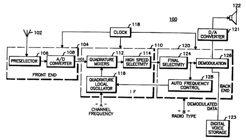
Figure 1 illustrates the functions of a digital receiver, comprising three
major operations. While the diagra n shows no example of receiver diversity, it will
be obvious to one skilled in the art that various diversity approaches could be applied
for use in a receiver of the present invention. In particular, the "front-end" section
104, which is further detailed in Figure 2, interfaces an antenna 102, receiving an
analog radio-frequency (RF) signal, to the digitally implemented ~ selectivity
section 110. The preselector 106 provides wideband filtering of the incoming
signal, to prevent aliasing in the subsequent AtD conversion process. The A/D
block 108 includes the gain and sample-and-hold operations necessary for the digital
processing of the present receiver structure.
The next major section, IF selectivity section 110, further detailed below in
conjunction with Figure 3, provides a quadrature local oscillator (LO) 116 whichgenerates a complex exponential signal (quadrature signals sine and cosine). Thefrequency of this signal is selected by the system channel frequency input"A". The
quadrature mixers 112 use digital multipliers to frequency-shift the desired
narrowband channel down to the IF frequency of approxirnatly zero Hz. The
high-speed selectivity section 114 includes several cascaded narrowband lowpass
filter sections, which remove undesired signals at higher frequencies from the
desired signal which is centered near zero frequency. This lowpass filtering permits
2 5 gradual sampling rate reduction from the high rates at the output of the A/D converter
108 to rates comparable to the channel bandwidth at the input to the "back-end"
section 120.
The "back-end" section 12û is used to "specialize" the general-pulpose radio
structure into one specifically tailored to a particular radio application, designated by
a system radio-type input "B". Its best implementation may comprise a
general-purpose digital signal processor (DSP). The final selectivity section 124
provides any additional fillering needed prior to demodulation of the radio signal in
accordance with the type of modulation and channel characteristics. For example, it
may provide adaptive channel equalization for a digital data communications
system. This filter section 124 also provides adjacent channel attenuation, and
i30~86
passband equalization to compensate for imperfections in the characteristics of the
high-speed selectivity filters 114, resulting from the coarse coefficient quantization
needed to implement multiplierless (lowpass) filters. The demodulation section 126
may be software-programmed to implement many types of demodulation, including
05 FM demodulation for voice and frequency-shift-keyed (FSK) data. The
demodulated voice signal may be converted back to analog form, then amplified and
played through a loudspeaker, as suggested by icons 121 and 122. Alternatively, a
digital voice message may be stored in digital a digital memory 123 for later
playback. In a data communications system (not shown), the demodulated data
lO symbols may be routed to a computer for further processing or to a computer
terminal for immediate display. In addition, control inforrnation to implement
automatic frequency tracking 128 may be generated in the "back-end" section 120.Finally, a clock-generation section 118 is required to control the input sampling rate
of the A/~ conversion as necessary for accurate down conversion, to operate the
15 digital circuitry in a regular fashion, and to control the output sampling rate, perhaps
for synchronizing with subsequent systems. In the exemplary embodiment to be
described here, the sampling rate fs is taken to be 20 MHz, and the band of
frequencies to be received is centered at approximately 875 MHz.
Figure 2 is a schematic diagrarn of the front end circuitry of the digital
20 receiver of the present invention. This circuitry functions to digitize a selected band
of radio frequency signals. The present invention provides that sampling is donedirectly at R.F. frequencies. However, wideband pre-selection is provided by R.F.
analog filters prior to sampling. The function of the R.F. filters 202 and 206 is to
provide selectivity to spurious responses. These spurious responses included the
2 5 image, half I.F. spurs, Able-Baker spurs, etc. as found in a conventional receiver
front-end. In addition to these spurs, selectivity must be provided to frequencies
which can be aliased by the sampling process. Maximum allowable bandwidth is
limited to the Nyquist bandwidth (fs/2, where fs is the sampling rate), althoughpractical filters will significantly reduce this.
Use of a 2-pole and 5-pole filter as shown in Figure 2, each with
bandwidths of approximately 4 MHz, will provide greater than 90 dB rejection to
aliased frequencies when sampled at a 20 MHz rate. In addition to providing
selectivity to signals entering antenna 224, filter 206 bandlimits wideband noise
entering the first sample and hold 208 generated by R.F. preamplifier 204. This is
necessary to prevent aliasing of noise, thus effectively increasing the noise figure of
the front-end 200. R.F. preamplifier 204 is used to amplify the R.F. signal to asufficient leve~ to provide the necessary signal-to-noise ratio needed for system
1304786
sensidvity. Since different filters are needed for different bands, it is practical to
include the R.F. amplifier 204 as part of the ~1lter structure (202 and 206). The
receiver of the present invention provides an R.F. ampli~ler 204 having a gain of
approximately 2~ dB and a noise figure of approxirnately 5 dB.
05 Clock 212 and sampling pulse generator 210 provide clock signals and
sampling pulses to the first sample and hold 208, second sample and hold 220, the
analog to digital converter 222, and the digital zero-IF selectivity section (not
shown). Clock generation may be accomplished by a 20 MHz crystal oscillator,
which is widely available. A 40 MHz signal for use by the digital signal processor
(not shown) is derived by doubling the 20 ~H~ signal by an analog doubling
circuit.
The pulse generator 210 is used to shape the 20 MHz clock signal (an
approximate sinusoid) into very narrow pulses. The width of the sampling pulse
depends on the highest frequency band desired to be received. A pulse width of
approximately 300 psec. will generate a "comb" of harrnonics with approximately
uniform amplitude to approximately 1 GHz. This is necessary for operation at theoperating frequency of approximately 875 MHz of the receiver of the present
invention. Pulse generation may be accomplished using a conventional step
recovery diode and ringing circuit. A circuit of this type is described in a publication
entitled Harmonic Generation Using Step Recovery Diodes and SRD modules,
Hewlett Packard Application note #920, available from Hewlett Packard Microwave
Serniconductor Division, 350 Trimble Rd., San Jose, Ca., 95131.
The band of signals amplified and selected by blocks 202, 204, and 206 is
sampled by the first sample and hold 208. This is analogous to down-converting in
a conventional R.F. receiver. Although a flash analog-to-digital converter
effectively sarnples the signal, practical converters have bandlimited inputs, thus
requiring sampling prior to conversion. Also, to date, all known high resolution (>
10 bits), high speed converters utilize a two-step conversion process. This type of
converter necessitates the use of a second sample and hold circuit 220.
Double sampling is necessary to overcome the practical limitations of
acquisition time, accuracy, and droop. The first sample and hold must acquire
extremely fast, in the r~nge of 300 psec in the receiver of the present invention. This
requires the use of a small hold capacitor in order to charge the capacitor fromsample to sample to approximately the voltagé of the input signal. The inability to
completely charge in the sampling interval to the value of the input signal results in a
mild filtering processing which can be considered negligible for narrowband signals
typically used for land mobile communications. The use of a small hold capacitor in
i31~)4786
the first sample and hold results in a droop ratc unacceptable for use by a two-step
analog to digital converter. Also, settling time of a relatively simple hold circuit as
can be used by the first sample and hold may be inadequate for a two-step converter.
For these reasons, a high accwacy second sample and hold 220 is used. Since the
05 signal has been effectively down converted, it is changing at a much slower rate.
This allows the use of a larger acquisition time and larger hold capacitor. Rnown
two-step converters require the sample and hold to droop less than 1/2 the step size
in significantly less than the sampling period (typically less than 1/2 the sampling
period).
The first sample and hold (208) may be implemented according to
conventional techniques using a Schottky diode bridge and a dual gate MOS FET asthe buffer arnplifier. The second sarnple and hold may be realized using a Schottky
diodc bridge, with additional back biasing to li~ut droop in the hold mode. A high
speed amplifier consisting of J-FETS in differential configuration as inputs and high
15 dynarnic range bipolar followers serves as a buffer amplifier.
Wideband amplifier 209 is necessary to further amplify the signal in order to
overcome the quantization noise of the analog to digital converter. The amplifier 209
is used to amplify a sampled signal; hence it must be wideband. High dynamic
range is also necessary to prevent amplifier nonlinearities from distorting the signal.
20 The amplier 209 noise figure is dependent on the amount of "takeover" gain
provided~F. amplifier 204 and overall noise requirements for sensitivity. A
Motorol 591 CATV wideband amplifier is suitable for use as the wideband
amplifier with the 800 MHz receiver of the present invention. An A/D converter
structure similar to the type described herein is shown in an article by Muto, Peetz,
25 and Rehner entitled Designing a 10-bit, 20 Ms-Per-Second Analog-to-Digital
Converter Sys~em, HEWLErr PACKARD JOURNAL, Vol 33, #11, pp. 9-29, Nov
1982.
According to the teachings of the present invention, a dither signal 218 is
added to the sampled signal at combiner/isolator 214. The combiner/isolator helps
30 prevent nonlinearities present in the wideband amplifier and dither source from
translating the low passed noise to other frequencies. The purpose of the dither 218
is to uniformly spread quantization noise of the analog-to- digital converter. The
uniform spreading of the noise floor over the Nyquist bandwidth prevents
intermodulation distortion caused by quantizing from being an inherent problem, and
35 also allows signal recovery below the least significant bit level, thus reducing gain
requirements before the A/D converter and easing the problems caused by
non-linearities in the stages preceding the converter. The dither signal 218 must be
i304~B6
added before the second sample and hold 220 if a two-step converter is used since
the signal must be held constant during the conversion period. The dither source218 can be realized by using an analog noise source such as a noise diode. The
general characteristics and advantages of dither signals are described in a paper by
05 Schuchman, L., Dither Sign41s and 7heir EJ~ect on Q~antization Noise, IEEE
TRANSACTIONS ON COMMUNICATIONS TEC~OLOGY, PP. 162-165, Dec. 1964.
Noise added to the signal should be spectrally isolatçd from the information.
The sampling performed in the 800 MHz receiver of the present invention places the
inforrnation approximately between 3 and 7 MHz. Low pass filter 216 prevents
10 noise from being added to the information signal. The receiver of the presentinvention is provided with a 5-pole elliptic filter with a 1.5 MHz cutoff frequency for
low-pass ~llter 216. The average voltage level of the dither signal over the noise
equivalent bandwidth of the low pass filter 216 should be greater than approximately
S step sizes of the analog to digital converter. Care must be exercised to prevent the
15 dither signal from causing clipping at the A/D converter 222.
The analog-to-digital converter 222 converts the analog signal to a digital
signal. The converter must be capable of accepting signals over the dynarnic
environment of the intended receiver application. For the land mobile
communications application, a rninimum of 10 A/D bits is necessary, and theoretical
20 studies indicate the dynamic range provided by a 12-bit converter should be
comparable with all existing conventional land-mobile receivers. The two factors of
prime importance of the analog to digital converter 222 are sampling speed and step
size. The step size determines the amount of gain necessary prior to the converter in
order to take over the quantization noise floor. The larger the step size, the larger the
25 gain requirement. Large amounts of gain result in nonlinear effects prior to the
converter. Conversion speed is also very important since this determines the
allowable bandwidth of the front-end filters, and also reduces the gain requirement
by spreading the quantization noise over a larger bandwidth.
An analog to digital converter 222 satisfactory for use with the 800 MHz
30 digital receiver of the present invention is a two-step 10-bit converter with a step size
of approximately 3 mV, which is capable of converting at rates greater than 50
MHz. According to the principles of the present invention, a front end gain of
approximately 54 dB is necessary to realize a post detection signal to noise ratio of
approxirnately 10 dB in a receiver having a 30 kHz bandwidth when receiving a 0.3
35 ~v signal sarnpled at a 20 MHz rate. The large amount of gain necessary prior to
converter 222 limits the nonlinear performance of the system. Interrnodulation ratio
(1~) is limited to approximately 65 dB which is somewhat less than that achievable
1304786
by conventional receivers. It will be obvious to one of ordinary skill in the art that a
reduction of the step size to approxirnately 200,uV will allow an lMR > 80 dB to be
achieved. This value is comparable with most existing conventional 800 MHz
receivers.
o 5 Referring now to Figure 3, a digital zero-IF selectivity section (DZISS)
compatible with the practice of the present invention is depicted in block diagram
form. The digital zero-IF selectivity section is disposed between the front-end
circuitry 200 of Figure 2 and the backend DSP 120 of Figure 1, and it operates to
convert the modulated digital RF signal output by front end 200 to the baseband
signal processed by the backend DSP 120. The DZISS 300 is cornprised of an
in-phase rnixer 304, a quadrature-phase rnixer 306, a digital quadrature local
oscillator (L0) 302 (providing an in-phase L0 signal 309 and a quadrature phase L0
signal 311), two "fast" digital lowpass filters 308 and 310, two "slow" digital
lowpass filters 312 and 313, and a clock source (not shown).
In the practice of the present invention identical digital information is applied
to both the in-phase mixer 304 and the quadrature-phase mixer 306 at input ports303 and 307 respectively. Generally, ports 303 and 307 are not single lines, but are
in fact multiple lines representing a multi-bit (e.g., 10 or 12 bits) digital word. The
actual length of the digital word used in any given application is dependent upon
many factors, including: the resolution required, the dynarnic range required and the
frequency of sampling the received RF signal. For example, a word length of 12
bits is considered to have an acceptable performance in receiving a typical radio
signal sampled at 20MHz.
Mixers 304 and 306 have as a second input quadrature L0 lines 309 and
311, respectively. As with the A/D output signal discussed above, the L0 signalsare not single connections, but are multi-bit discrete time representations of signals
- that are 90 degrees apart in phase (i.e., sine and cosine waveforms). Mixers 304
and 306 perform arithmetic multiplications of the A/D input word and the L0 word,
rounding the result to form an output word that is applied from the output ports of
30 mixers 304 and 306 to the input ports of digital lowpass filters 308 and 310,respectively. The digi~al word lengths of the LO and mixer output signals may beselected to yield acceptable noise performance. As the digital word is lengthened,
more quantization levels are available to represent the signals. The smaller
quantization increments lead to improved noise performance, as is well understood
35 in the art. This quadrature mixing process described above is analogous to that
performed in an analog "zero-IF', or direct conversion receiver.
i~O4786
1G
However, the use of truly linear digital multipliers precludes second order m~xing of
undesired signals
to D.C., and other undesirable effects, as occurs with analog direct conversion.05 The quadrature mixing performed by multipliers 304 and 306 acts to
frequency-translate the desired signal to a center frequency of approximately zero
Hz, where the amount of frequency translation maybe determined by channel
frequency control 305. The resultant quadrature signal may then be lowpass filtered
to remove out-of-band noise and undesired signals. In the preferred practice of the
present invention, this selectivity is provided in two stages. The first stage is
formed by fast recursive digital ~llter sections 308 and 310. Digital filters 308 and
310 are identical in structure and may be formed from a recursive filter topology
which will be described below in greater detail. The remaining selectivity is
provided by "slower" recursive filters 312, and 313, respectively. This choice of
architecture will be discussed in more detail below. Following the filtering process,
the digital signals are output to a backend DSP 120 for further processing.
Figure 4a is a schematic and block diagrarn of the digital oscillator described
in conjunction with Figure 3. Recall that the function of the quadrature oscillator is
to provide digitized, sampled versions of the cosine and sine waveforms utilized in
the quadrature mixing process. Implementation of the digital zero-IF selectivitysection depends on the ability to generate accurate, stable digital representations of
these waveforms. A class of digital oscillator realizations particularly suited to the
requirements of the present invention is based on the concept of ROM (read only
memory) lookup. Consider the generation of a digital signal comprising samples of
2 5 the complex sinusoid:
w(t) = ei27~fct
where fc is the desired oscillator frequency.
According to conventional communications theory,
3 5 ej2~lfct = cos2~1fct + jsin2~1fct,
. ~ ,
~304786
1 1
Thus the desired cosine and sine waveforms may be regarded as the real and
imaginary parts, respectively, of the complex sinusiod waveform. The sampled
version of ei2~fct is obtained by replacing the continuous time variable t by the
discrete time variable nT, where n is a counting integer (1,2,3, ...) and T is the
05
sarnpling period, which equals l/fs = l/sampling rate. This discrete time signal is
then equivalent to:
w(n)= ei27~fc(nT)
ROM lookup methods of generating this signal follow from making the
frequency variable fc~ as well as the time variable, discrete. If we let fc = kf5/2N
(where k and N are integers), then:
w(n)= ei2~kfS(n/fs)/2N=ej2~nk/2N
It can be seen that cosine and sine values for only 2N different phases need
be generated. One method of generating these values, called direct ROM lookup,
basically involves the use of ROM table containing the 2N pairs of values (cosine
2 o and sine), which is addressed by a register containing the integer nk (proportion to
phase.) The phase register is incremented by the incremented by the value k
(corresponding to the desired frequency fc) at each sample time (corresponding to
n). The frequency resolution obtained is ~f = fS/2N, wherein 2N distinct frequencies
can be generated.
Depending on the application, the direct ROM look-up technique may
involve large amounts of ROM. The ROM size may be reduced somewhat by taking
advantage of the symmetric properties of cosine and sine waveforms. Such
properties allow the number of table entries to be reduced from 2N, to 2N/8, pairs of
numbers. Even with this reduction the ROM size may still be excessive. In such
3 o cases, a technique called Factored ROM lookup may be employed to further reduce
ROM size.
The digital local oscillator 400 of the present invention uses the factored
ROM look-up technique utilizing the fact that the unit magnitude phasor can be
broken into a complex product of "coarse" and "fine" phasors. Thus, the unit
magnitude phasor ei0 can be represented dividing the signal into ei0c eJ0f.
Therefore, the unit magnitude phasor can be realiæd by having separa~e
~304786
coarse value phasors and fine-value phasors stored in ROM which are multiplied
together to get thediscrete time sine and cosine values required for the quadrature
mixers. The advant.~ge of this factorization is that the amount of ROM necessary to
store the coarse-value and fine value phasors is greatly reduced from that required
05 for the direct ROM look-up approach. The expense paid for this ROM size
reduction is the introduction of circuitry to perform the complex multiplication of
coarse and fine phasors. Generally, a complex multiplication can be implemented
with four multipliers and two adders. By proper selection of the fine-value phasor,
and recalling that the cosine of a small angle can be approximated by one, the ROM
l0 for the cosine fine-value phasor can be eliminated. Further, by approximating the
small angle cosine values as one, two multipliers can be eliminated from the
multiplication structure required to generate a complex product. This results in both
a cost and size savings in the factored ROM implementation.
Referring still to Figure 4a, the digital quadrature local oscillator 400, as
15 implemented using a factored-ROM approach, is depicted in block diagram form.Frequency information, in the form of an N bit binary number proportional to thedesired frequency, within the band sampled by the A/D converter, is loaded into the
channel frequency latch 402. Channel frequency latch 402 may be realized in manydifferent forms. For example, assuming that N=20, five cascaded 74LS175's
20 (Quad D flip-flops), manufactured by Motorola, Inc., and others, provide an
acceptable implementation. Those skilled in the art will appreciate that channelfrequency latch 402 may be loaded by various means. For example, in a single
frequency radio the channel frequency latch could be permanently loaded with a
single binary number. For multiple frequency radios, channel frequency latch 402
25 could be loaded from an EPROM or ROM look-up table or else calculated by and
latched from a rnicroprocessor.
The output of channel frequency latch 402 is coupled to a binary sumrner
404. It will be understood by those skilled in the art that in the following discussion
of digital quadrature local oscillator 400 all coupling lines in between the functional
30 blocks are in fact multi-bit binary words and not single connections. The output of
adder 404 is coupled to phase accumulator 406. Phase accumulator 406 can be
implemented as an N-bit binary latch which is used to hold the address of the next
location of ROM to be addressed. Thus, the output of phase accumulator 406 may
be directly coupled to cosine coarse-value ROM 418, sine coarse-value ROM 416,
35 and sine fine-value ROM 414 (recall that fine-value cosine ROM is not required, as it
is being approximated by one). Further, the output of phase accumulator 406 is fed
back into summer 404 to be added (modulo 2N) to the binary number representing
~30~78
the channel frequency inforrnation located in the channel frequency latch 402. The
output of phase accumulator 406 is updated once every clock pulse, which is
generally the sampling frequency. The result of this binary addition is that phase
accumulator 406 is holding the binary sum (proportional to phase) of the last address
0 5 plus a binary vector contained in the channel frequency latch. This number indicates
the next address to be required to create the quadrature local oscillator signals cos
27~fcnT and sin 21~fcnT.
In the preferred embodiment, the ROM size may be reduced, or
equivalently, the frequency resolution may be improved without increasing the ROM
size, by adding a digital dither signal to the output of phase accumulator 406 and
truncating the result prior to addressing the ROM tables. The frequency resolution
of the local oscillator is defmed by the data path width (N) of the phase accumulator
and the sampling rate fs required. The most straight-forward method of increasing
frequency resolution is to add more bits to the phase accumulator and increase the
size of the ROM tables. However this can be an expensive solution since the ROM
must double in size for each bit added to the phase accumulator. Another option
would be to add bits to the phase accumulator but truncate the additional bits before
performing the ROM look-up. This introduces severe phase rounding and causes
spurs in the local oscillator output. In order to avoid these spurs a low level dither
signal is added to the accumulator output before truncation.
According to the principles of the present invention, the frequency
resolution of the digital oscillator may be enhanced, without increasing ROM size
and without introducing spurs in the output, by adding a binary dither signal to the
output of phase accumulator 406 before truncating. To accomplish this, digital
oscillator 400 is provided with an L-bit dither source 408, which generates an L-bit
wide, uniform probability density, pseudorandom "white noise" signal. Dither
source 408 is clocked at the sampling frequency f5 so as to provide a new L-bit
dither word for every phase word output from phase accumulator 406. An N-bit
dither word is formed by appending M = N - L leading zeroes to the L-bit dither
word output from dither source 408. This composite N-bit dither signal is added to
the N-bit output of phase accumulator 406 by N-bit binary adder 410, in Modulo 2N
fashion. The sum output of adder 410 is then truncated to M bits (truncation notshown). In practice this truncation process is achieved by simply ignoring the least
significant bits produced at the output of digital adder 410. The truncation operation
itself allows for reduced ROM size.
Quantization or ~uncation of the binary phase word produces distortion or
noise in the generated sine and cosine waveforms. Since the phase is a periodic
1304786
function (sawtooth), the noise produced by quantization would also be periodic
unless it is randornized somehow. Periodic noise would result in discrete "spurs" in
the oscillator output spectrum which are undesirable in most applications if their
level exceeds some threshold. Addition of the dither signal prior to phase
0 5 quantization randomizes the phase noise, resulting in a more desirable white noise
spectrum at the output. The binary phase word is represented by a binary word of N
bits. The dither signal comprises a pseudo-random binary word of L bits which issummed with the N bit phase word. The process results in a binary word N = L +
M bits. This binary word is then truncated to a binary phase word of M bits which
10 is relatively free of the spurious signals described above.
The effect of phase quantization on oscillator output noise can be shown by
the following analysis. The desired oscillator output is described by the following
equation:
w(n) = ei2~fCnT = ej0(n)
If the phase angle is quantized with error a(n), the actual output is described
as follows:
w(n) = ei[0(n)+a(n)]
The error introduced is:
E(n) = w(n) - w(n) = ei[0(n)+a(n)] - ei0(n)
= ei0(n) [eia(n)- 1]
For the case of interest where a(n) is very small (~< l), eia(n) can be
approximatedby l+ja(n),thusyielding:
E(n) = ei0(n) j~(n)
The spectrum of E(n) can be seen as simply a frequency translation (and
unimportant scaling by j) of the spectrum of the phase quantization noise ~(n). Thus
if a(n) is random or "white", so is E(n). Furthermore, the power of E(n) equals the
power of a(n), allowing the output noise level created by the phase noise to be easily
3 5 estirnated.
Choosing the power level of the dither signal involves a tradeoff between
noise whitening effect and output noise power level. As the dither power is
~30~786
increased (by increasing the number of bits, L, in the dither signal), the noisebecomes more whitened, but the total phase noise power increases as well. It can be
shown that if the dither signal exhibits a uniform probability density,
the choice of L = N-M results in the preferred level of dither power since it
05 represents the smallest dither signal necessary to completely whiten the phase
quantization noise. Thus, in the preferred implementation, the number of dither bits
L equals the number of bits discarded in the truncation process. It may be notedthat dither signals exhibiting other than uniform probability density may be utilized.
However, a uniform density is preferred as it is the most easily generated. With10 L = N-M, the variance ~power) of the phase noise is equal to 2 times the equivalent
phase variance of the dither signal. Given a desired frequency resolution,
determined by N and fs~ then L and M, and hence the required ROM size, are
determined by the allowable level of white noise at the oscillator output.
As an example, with fs = Z MHz, and N = 20 bits, the frequency
resolution is 19.07 Hz. Truncating to M=17 bits (to reduce ROM size by a factor of
8) without dither creates spurs in the oscillator output, which for one particular
frequency are 98 dB below the level of the desired signal. Addition of a 3-bit dither
signal prior to truncation whitens the error signal, eliminating the
spurs. According to the principles of the present invention, the frequency
2 o resolution of the digital oscillator, for a given level of output noise, can be increased
indefinitely by simply adding more bits to the frequency and phase latches, and to
the dither signal. The ROM size, determined by M, remains constant. The M-bit
binary word retained after truncation is coupled to the ROM address latch 412,
whose output is coupled to ROM's 418, 416, and 414. Upon receiving an address,
ROM's 418, 416, and 414 output the digital binary word located at the received
address on their respective output ports. The digital quadrature signals are then
arithmetically generated from the three binary numbers.
As stated previously, the output signals of ROM 416, and 418 are binary
numbers proportional to the cosine and sine of the coarse phase. The output signal
of ROM 414 is a binary number proportional to the sine of the fine phase. In order
to rninimize the error in the fine cosine approximation, the fine phase values used are
the values centered around the positive axis. The output of ROM address latch 412
~304786
16
is an M bit number that is divided into a Mc bit coarse address and an Mf bit fine
address where M = Mc + Mf. The coarse phase is 2~(Pc + 1/2) /2Mc, where Pc is
the integer corresponding to the Mc bit coarse address. The fine phase is 21~(pf -
2Mf-1)/2M, where Pf is the integer corresponding to the Mf bit fine address. For05 example, if Mc = 10 and Mf = 7, the ROM table enhies may be configured as
shown below in Tables 1 and 2.
Address (Pc) I Contents of I Contents of
coarse COS ROM I coarse SIN ROM
a~addresS Pc I at address 'P
O I COS 2~-(1)/211 I SIN 2J~-(1)/211
cos 2~-(3)/211 I SIN 2~-(3)/211 1
1 2 I COS 2~-(5)/211 I SIN 2~1-(5)/2
3 I COS 2~-(7)/211 I SIN 27~-(7)/2
4 I COS 2~-(9)/211 I SIN 2~-(9)/211
I I I I
;022 I COS 2~1(204S)/2ll I SIN 27~(20~)/2
1 1023 I COS2~(2047)/2ll I SIN2~(2047)/2
TABLE 1
_
Address (Pf) I Contentsof
fine Sl:N ROM
1 1 at address 'p~!
O I SIN 2~ 64)/2l7
SIN 2~ (-63)/217
2 I SIN 27~(-62)/2l7
3 I SIN 2~(-61)/217
;26 I SI~ 2Tt(62)/217
127 I SIN 21~(63)/217
l_
TABLE 2
130~786
17
To generate the cosine waveform (i.e., the real component of the complex
waveform), the outputs of sine coarse-value ROM 418 and sine fine-value ROM 414
are f~rst multiplied in multiplier 426. The output of multiplier 426 is fed to summing
circuit 440 where it is subtracted (2 s complement form) from the output of cosine
05 coarse-value ROM 416. This arithmetic process yields the cosine-value which is
output on port 441 and coupled to quadrature mixer 304 of Figure 3. To generate
the sine values of the digital quadrature L0 the outputs of the cosine coarse-value
ROM 416 and sine fine value ROM 414 are multiplied in multiplier428. The output
of multiplier 428 is fed to a summing circuit 442 where it is surnmed with the output
of sine coarse-value ROM 418. Sumrning circuit 442 outputs via connection 443 the
discrete time sine value digital word which is coupled to quadrature mixer 306 of
Figure 3. Therefore, since the discrete time values of the sine and cosine signals are
calculated mathematically, perfect 90 phase control is achieved using minimal ROM
space. Latches 420, 422, 424, 434 and 438 provide pipelining which facilitates
high operating speed of the digital oscillator. Delays 430 and 436 are provided to
equalize the delays of the various signal paths.
The factored ROM LO reduces the ROM area while maintaining acceptable
frequency resolution. For example, to implement a digital quadrature LO that
operates at 20 MHz, the coarse-value ROM's 416, 418 could each be implemented
in a 1024 x 16 ROM and the fine-value sine ROM 414 could be implemented in a
128 X 8 ROM. This would result in frequency resolution of approximately 20 Hz
using approximately 34,000 bits of ROM. The factored-ROM configuration is
preferred for operation at high sampling rates, since, except for the phase
accumulator, there is no circuitry connected in a feedback manner. This allows the
2 5 rest of the LO circuitry (especially multipliers 426 and 428, which represent the main
speed bottleneck) to be pipelined to achieve a very high operating rate. Pipelining
would consist of introducing latches at certain critical points, such as within the
multipliers themselves, as is well understood in the art. Thus, a factored-ROM LO
is described which outputs discrete time digital quadrature signals which exhibit a
selected frequency.
A digital adder suitable for use with the apparatus of the present invention
may be of a type constructed with several 74LS181 4-bit arithmetic logic unit
devices, connected in parallel. These devices are shown and described in a data
manual entitled "Motorola Schottky TTL Data Book", avaliable from Motorola, Inc.,
Box 2092 Phoenix, Arizona, 85036. ROMs 418, 416 and 414 may be formed by a
variety of well known ROM devices such as a 82LS181 available from Signetics
Corporation, 811 E. Argues Avenue, P.O. Box 3409, Sunnyvale, Calif. 94088, and
i304786
described in the "Signetics Bipolar Memory Data Manual", 1984- Both multiplier
42~ and 428 may be realized as, for example, an MPY016K manufactured by TRW,
Inc., TRW Electronic Components Group, P.O. Box 2472, LaJolla, Ca. 92038.
The amount of coarse-value ROM required can be further reduced by taking
05 advantage of symmetries in the cosine and sine wave forms, and thereby storing
only the values of the unit magnitude phasor residing in the first octant (i.e., the first
45) of the phasor unit circle. Those skilled in the art will appreciate that the unit
magnitude phasor represents sine or cosine values rotating through 360. Due to the
symrnetrical nature of sinusoidal waveforms, the values of the cosine and sine
waveforms over the first octant of the unit circle are identical to the values of these
waveforms over any other octant, except for possible sign changes and reversal of
roles (i.e., sine becomes cosine and vice versa). Therefore, the only coarse-value
phasors that are required are those in the first octant provided there is an indicator of
which octant the phasor is currently residing, and there is circuitry present to negate
(i.e., change sign) and/or exchange the outputs of coarse-cosine ROM 416 and
coarse-sine ROM 418 according to the current octant. An octant indicator is readily
implemented using three binary bits of the ROM address. For example, the three
most-significant-bits (MSB's) could be used to indicate the octant, and the remaining
bits used to address the ROM for the coarse-valued phasor.
Figure 4b is a schematic diagram of an example of a type of digital dither
generator compatible with the digital oscillator of the present invention. A digital
dither signal can be generated by any of several well-known pseudorandom
sequence generation techniques. One type of dither, or random number generator is
shown and described in a paper by G. I. Donov, A High-Speed Random-Nu~ber
Generator, RADIO ELECTRONICS AND COMMUNICATION SYSTEMS, VOI. 25,
No.4, pp. 88-90, 1982.
Referring now to Figure 4b, a feedback shift register pseudorandom
sequence generator which may be advantageously employed in the practice of the
present invention is shown in schematic form. The sequence generator of Figure 4b
is used to provide an L-bit digital dither signal to the binary adder 410 of Figure
4a. The dither generator 408 includes an R-bit shift register 460 which may be
formed of a plurality of flip-flops 464 through 499 which are connected in a cascade
fashion. In the preferred practice of the present invention, a parallel 3-bit dither
signal is tapped from the shift register at the outputs of flip-flops 478, 491 and 499
respectively. The inputs to an Exclusive-Or gate 462 are coupled to the outputs of
flip-flops 464, 493, 498 and 499. The output of Exclusive-Or gate 462 is coupledto the input of flip-flop 464. The shift register produces a 3-bit pseudo-random
i304786
19
dither signal which is added to the output of the phase accumulator 406 of Figure
4a. The flip-flops 464-499 and the Exclusive-Or gate 462 as well as the other
devices used in the practice of the present invention may be any of several wellknown logic devices; however, high speed l~L devices are particularly well adapted
0 5 for the practice of the present invention. Implementations employing other logic
families will also be obvious to oDe of ordinary skill in the art. The dither generator
of Figure 4b is set forth as an example of one type of digital dither generator which
performs satisfactorily with the digital oscillator of the present invention. It would
be obvious to one skilled in the art that many other digital dither generators could
also be advantageously employed, provided the digital dither generator provides a
pseudorandom sequence of L-bit numbers whose period is at least as long as 2N
samples, and whose probability density is uniform, in order for the phase noise
produced by truncation to be "whitened".
As shown in Figure 3, the intermediate-frequency (IF) filter section accepts
data from the A/D converter at the rate of 20M samples/sec, mixes the received
signal to dc (the zero IF frequency), lowpass filters the received signal to extract the
desired signal, and sends the signal to the backend 120 of Figure l at a (drastically)
reduced sampling rate. In the preferred implementation, the lowpass filtering and
sample-rate reduction are not separate operations; instead, the sampling rate is2 o gradually reduced between filter sections, as undesired signals (which could cause
aliasing if not removed) are filtered out. The only filtering section which operates at
the input sampling rate (fS=20 MHz in the exemplary embodiment described here) is
the first section. The only other circuitry which operates at that rate are the
quadrature local oscillator (LO) and mixers. Thus it is this high-speed circuitry
which sets an upper lirnit on the overall operational speed of the digital zero-IF
selectivity section. High-speed operation is very important to the digital receiver of
the present invention, to minimize intermodulation problems occurring with the
front-end sample-and-hold and A/D converter and to allow a sufficiently wideband
signal to be accepted.
Figure Sa is a block diagram of the "fast", narrowband lowpass filters 308
and 310 of Figure 3. The quadrature local oscillator 302 and mixers 304 and 306
are non-feedback circuits (primarily ROMs and multipliers) which are amenable topipelining or other forms of parallelism to in~rease their speed. However, because
the lowpass filter sections 308, 310 are implemented as recursive (infinite impulse
response) filters, they cannot be pipelined to increase their speed. Their speed is
determined by the maximum delay around a closed (feedback) path. For the
lowpass filter implementation of the present invention, this path includes two digital
304786
adders and one latch. It is this path which limits the A/D sampling rate and,
therefore, potentially limits the overall performance of a digital receiver. Because of
problems in atta~ning this very high speed the filter was designed by interleaving two
l~Iz TIL filters. The aliasing problems that would ordinarily be associated witho 5 using a lower sampling rate are alleviated by adding zeroes near the unwanted filter
poles.
The "Fast" lowpass section 546 of Figure Sa is decomposed into two
half-speed sections plus a combining filter, as is shown in Figure Sb. This
modification permits the digital IF section to operate at twice the speed that would
10 otherwise be possible, and potentially allows improved perforrnance of the digital
receiver of the present invention. The "decomposed" filter of the present invention
is shown in conjunction with Figures 3 and 5. Other filter decomposition techniques
have been discussed, for example, in a paper, ~. Bellanger, G. Bonnerott and M.
Coudreuse, Digital Filtering by Polyphase Network: Application to Sample-Rate
15 Alteration and Filter Banks. EEE TRANSAC tlONS ON ACOUSTICS, SPEECH, AND
SIGNAL PROCESSING, Vol. ASSP-24, No. 2, April 1976.
The combining filter 554 is a nonrecursive filter. The combining filter,
which is shown in greater detail in Figure 8, uses two zeros at fS/2 (z = -l) to cancel
the poles introduced by the decomposition. Such a filter can be implemented with
20 only adders and latches (i.e., without multipliers), and so adds minimal hardware.
Note that although decomposition requires additional hardware, it nominally
increases power consumption (with a CMOS implementation), since two half-speed
circuits require approximately the same power as a single full-speed circuit.
(ignoring the additional power of the combining filter.
Figure 6 illustrates the decomposition process in detail with several
magnitude plots. In particular, Figure 6a shows the response of the original version
of the first two-pole section, for an input sampling rate fs f 20 MHz. Figure 6b
shows the "decomposed" characteristic which results from two l0-MHz sections,
while Figure 6c shows the response of the subsequent "combining" filter. Finally,
3 0 Figure 6d shows the composite (i.e., cascade) of Figure 6b and Figure 6c, which is
virtually indistinguishable from Figure 6a, except for the "notch" at l0 MHz (which
results from the two zeros at fs /2, which cancel the two nearby poles).
The decomposed filter can be represented as follows:
3 5 2ND
y(n)= y(n-i)hd(i)+x(n)
1 =1
~304'786
21
where x and y are complex filter inputs and outputs, respectively (i.e., they have
both a real part and an imaginary part). Also, hd are the decomposed filter
pc,lynomial coefficients, and ND = 2 is the order of the original full-speed filter.
Since the decomposed 20-MHz filter is expressed in terms of z-2 (as will be shown
05 in the next section), it can be implemented in terrns of a 10-MHz circuit wherein:
hd (i ) = hh (i /2), i even
0, i odd
where hh are the original high speed coef~lcients.
15 Then the decimating flter can be reexpressed as:
2ND
y(n)= ~: y(n-i)hh(i/2)+x(n)
i =2
step 2
The change of variables i fi 2j sirnplifies this summation to:
ND
y(n)= ~ y(n-2j)hh(j)+x(n)
j=l
From this formulation, decimating-filter inputs x and outputs y can be
decomposed into two streams, as shown in Figure Sa:
x(Y)(m)=~s(2m+y)
y ~Y)(m ) = y (2m +y)
where:
y = mod(n, 2) YOO {0,1 }
Substituting n fi 2m + 1 in the above decimating-filter summation yields:
ND
y(n)= ~; y(2m-2j+1)hh(j)+x(2m+y)
j=l
1304786
Finally, the two decomposed decimating filters ( y = 0,1) may be represented as:
ND
y (y)(m ) = ~ y (Y)(m j ) hh (i) + x (Y)(m )
05
j =l
Assume that the desired filter has a pole z = zp. Then the corresponding filter
characteristic may be represented as:
10H = (1 zp z -1) -1
If this pole is "repeated" 180 away, the following characteristic is obtained:
H ' = [(1 zp z -1) (1 - zp e i~ z -1)~ -1
--[(1 - z z ~1) (l + z z -1)]-1
Since the resulting characteristic is in terms Of z -2, it can be decomposed (as was
shown in the previous section) into two half-speed filters, each with pole z 2 = zp2.
25The lowpass filter sections in the digital zero-IF selectivity implementation of
the present invention is realized using the following form, which is written in terms
of coefficients a and b, where b = ca . For a pole-pair zp, zp*, where:
zp = (1-d )e iq (d, q 1)
the coeff1cients are:
30 a @2d
and
b = d2 + q2
For the half-speed filters, the pole-pairs are zp2 and (zp2)* Since
35zp2 = [(1-d ) eiq]2
@ (1-2d)ei2q
~30~786
23
Then the coefficients for the half-speed filter may be obtained in terms of those for the
full-speed case by analogy to the full-speed case:
a ' = 2(2d )
= 2a
5 and
b ' = (2d )2 + (2q)2
=4(d2+q2
= 4b
This design is illustrated in Figure 5b. A second-order IIR filter is described in
a paper, Agarwal, A.C., Burrus C.S., New Recursive Digital Filter Structures
Having Ve~ Low Sensitivit~ and Roundoff Noise, EEE TRANSACTIONS ON
CIRCUITS AND SYSTEMS, Vol. CAS-27, No. 12, Dec. 197',. The filter structure II
proposed by Agarwal and Burrus has been modified for minimum delay around all
lS feedback loops for the purposes of the present invention. The filter structure of the
present invention is illustrated in Figure 7.
All digital filter structures are made up of basically the sarne three components:
adders, multipliers, and delay circuits (generally latches or RAM). The factors
affecting the performance of a digital filter all have to do with the fact that the various
2 parameters of the filters are quantized, that is, they have finite precision rather than
the infinite precision available in analog filters. The finite precision of a digital filter
basically gives rise to three major performance effects that must be controlled in any
implementation of a digital filter.
Coefficient roundoff is one of these effects. The constant valued coefficients
25 found in a digital filter determine its frequency response. The result of rounding
these coefficients so that they may be represented digitally in a finite number of bits
causes a permanent, predictable change in the filter response. This is analogous to
changing the RLC values in an analog filter; however, digital filters do not suffer the
detriment of temperature variations as in analog filters. Generally, the higher Q of
30 the filter (i.e. narrow bandwidth compared to the sampling rate) the more the
frequency response is distorted by coefficient rounding, unless special structures are
employed. Judicious selection of the filter structure is of key importance in light of
the fact that IF filters a~e generally extremely narrow band, or high-Q filters.Round-off noise is another of the performance characteristics that must be
3 5 controlled in a digital filter. Data entering a digital filter has been rounded to a finite
number of bits, and it is almost always necessary to perform additional roundings at
1304786
24
certain points within the filter. Such rounding operations create an error or noise
signal in the digital filter. For exarnple, if the digital word length used in a filter is
16 bits and the coefficients are represented in 10 bits each multiplication operation
would create a 25 bit product, which must be rounded to 16 bits before the result
o 5 may be put back into memory.
The last major effect that is controlled in a digital filter is the overflow level.
The fact that data samples are represented in a finite number of bits means that there
is a maximum allowable absolute value associated with every node in the filter
which, if exceeded, results in an overflow phenomenon (generally wrap-around if
2's complement binary arithmetic is used). This largest allowed data value, coupled
with the level of roundoff noise described previously, deterrnines the dynamic range
of the filter.
Several conventional structures are available to implement digital filters. A
straight forward design approach is to cascade sections of first and second order
direct-fonn filters until the desired ~llter order is achieved. The advantages of this
method are its simplicity, regularity, and the ease of actual filter design. However,
the conventional approach also suffers from many detriments mostly stemming fromthe fact that high precision (for example 16 bit) filter coefficient representation is
required to implement a narrowband filter. This necessitates highly complex
2 o multiplications (for example 16 20 bits) be performed in the feedback paths of the
lter sections. The multiplications place severe speed and time limitations on the
operation of the filters. Further, pipelining, a common technique used to speed logic
circuits, cannot be employed in feedback loops. Lastly, high precision, high speed
multipliers consume tremendous amounts of power.
Referring now to Figure 7, a digital lowpass filter section 700 is depicted in
block diagram form. The filter employed in the DZISS is a recursive filter (i.e., the
output signal is fed back, scaled, and summed at strategic points in the filter
structure) having a narrow bandwidth and optimized for high-speed and
low-sensitivity to the previously described detrimental effects of parameter
3 o quantization on digital filters. The second-order narrowband lowpass
infinite-impulse response (IIR) filter of Figure 7 is used in the decomposed "fast"
lowpass filter of Figure 5b, which operates at the speed of the A/D converter.
Decomposition is useful in attaining this high operational speed, but requires
additional hardware: two second-order IIR sections instead of one, and a
3 5 second-order FIR section which would not otherwise be needed.
The digital low pass filter 700 provides the function depicted by the function
blocks 550 and 552 of Figure 5b. The digital lowpass filter 700 consists of four
~304786
digital adders (2's complement) 704, 708, 712, and 716, two digital delays or
latches 710 and 718, and two binary shifters 706 and 714. As mentioned previously
in the discussion of the digital quadrature local oscillator 400, the individualconnections of lowpass filters 308, 310, and 312, and 313, as described in Figure
0 5 3, are multi-bit digital words and not single electrical lines.
The input signal to the digital filter 700 is applied to a non-inverting input 702
of the digital adder 704. A second inverting input to the digital adder 704 is taken
from digital delay 718 which is fed back from the output 720 of the filter circuit.
The difference (2's complement) result of digital adder 704 is next applied to the
input of gain element 706 which presents the shifted first sum signal as one input of
digital adder 708.
Bit shifter 706 shifts all bits of the data word outputted from digital adder 704 to
the right (i.e., toward the least significant bit) by Nc bits, effecting multiplication by
a coefficient c equal to 2-NC. This bit shift may be implemented by an appropriate
routing of the data lines from digital ladder 704 to adder 708. Thus, high operating
speed of digital filter section 700 is facilitated, since there is no time delay associated
with bit shifter 706, as there would be in a coefficient multiplication implemented by
a conventional multiplier circuit.
Digital adder 708 adds to the shifted first sum signal the last output of digital
2 o adder 708 as held in delay 710. Further, the last or previous output of digital adder
708 is applied to digital adder 712. A second inverted input to digital adder 712 is
taken from digital delay 718 which, as previously mentioned, is taken from the
output 720 of the digital filter. The result of digital adder 712 is applied to bit
shifter 714 which is coupled to digital adder 716. Bit shifter 714 shifts a~l bits of the
data word outputted from digital adder 712 to the right by ~a bits, effecting
multiplication by a coefficient a equal to 2~Na. Bit shifter 714 also facilitates high
operating speecl since no eime delay is incurred. The parameters Nc and Na
associated with bit shifters 706 and 714 respectively, control the frequency response
of digital filter section 700, and may be chosen to yield the response appropriate to
the intended application, as shown by the previous analysis. Digital adder 716 adds
the second shifted sum signal to the previous output of 716 as held in delay 718.
The output of delay 718 is also the output of the digital lowpass filter section 700
and represents a band-limited representation of the input signal 702 that was
previously applied to the input of sumrning circuit 704.
Figure 8 is a block diagram of the second-order combining
imite-impulse.response (FIR) filter with a notch at half the sampling rate used in the
decomposed fast lowpass filters of Figure Sb. The input 802 to filter 800 is
~304786
26
coupled to the output 720 of filter 700, as pictured in Figure Sb According to
Figure 8, the digital filter 800 comprises digital shifters 804, 806, and 808 coupled
to digital delays 810 and 814 and digital summers 812 and 816, respsctively The
digital shifters 804, 806, and 808 use gains of 1/4, 1/2, and 1/4, respectively~ to
05 implement a filter with two zeros on the unit circle, at half the sampling frequency.
These digital shifters perforrn right shifting of the input 802 by 2, 1, and 2 bits,
respectively. Since such "bit shifting" may be implemented by routing the wiringconnections in the appropriate manner, these gain operations consume no actual time
and require no actual hardware. A first partial sum is formed in adder 812 using the
l0 scaled output of gain element 806 as the first input and the previous, or last, scaled
output of gain element 804 as the second input, obtained from delay element 810.Similarly, the output 818 is obtained as the second partial sum formed in adder 816
using the scaled output of gain element 808 as the first input and the previous, or
last, first partial sum of adder 812 as the second input, obtained from delay element
15 814. The transfer function of this filter may be written:
H(z) = Y(z) / X(z) = (1/4)[1 + z-l (2 + z~~)]
To compute an output, this FIR filter needs only to perform one addition and
one latch operation, compared with two additions and one latch operation in the IIR
sections, so that the FIR combining filter easily operates at the full input sampling
25 rate (20-MHz). An alternative design would allow the adder to run at a lower
sampling rate by the use of additional control circuitry. This would perrnit the F~R
filter to operate more slowly by incorporating decimation into ~he filter operation,
i.e., computing only the outputs needed by subsequent filter sections operating at a
reduced sampling rate. In a CMOS implementation, power consumption is typically
30 reduced when operational speed is reduced. Therefore, the power consumption of
the FIR combining filter could be reduced at the expense of some control circuitry.
Between the "fast" filters 308 and 310 and "slow" lowpass filters 312 and 313
of Figure 3, it is desirable to perfonn sampling rate reduction, or decimation. As is
well known in the art, the degree of sampling rate reduction possible depends on the
35 amount of attenuation provided by the "fast" lowpass filters. For example, if a 20
MHz input sampling rate is used, and the "fast" filters are implemented as
decomposed filters with coefficients as listed below in table 3, then an output
1~04786
27
sampling rate of 2 MHz can be used with over 100 Db of aliasing pro~ection
provided by the "fast" filters.
filter I Irate
05 I sectivn _ I a c ~(MHz!
fast(deco~osed) 1 2 8 2-9 1 20
slowl 1 2-6 2-2 1 2
slow2 1 2-6 2-3 1 2
SlOW3 1 2-6 2-4 1 2
I . I I . I
TABLE 3
The "slow" lowpass filters 312 and 313 can be implemented by several stages of
two pole filter sections. For example, if three stages, each having the structure of
l 5 Figure 9a, 9b, and 9c and the coefficients listed in Table 3 are used, wherein slow 1
slow 2 and slow 3 colTespond to Figures Pigure 9a, 9b, and 9c, respectively, then
the sampling rate can be reduced from 2 ~Iz to 80 KHz.
An alternative hardware-saving design involves interleaving the in-phase and
quadrature sample sarnple streams and using three stages of time-division-
2 o multiplexed filtering. This requires that the filters run at twice the rate they wouldoperate with a non-multiplexed design but since the sampling rate is reduced by a
factor of 10 from the fast filter, this multiplexed filter still can operate at one-fifth the
rate of the first filtering stage.
Figure 9a is a block diagram of the first time-division-multiplexed
2 5 second-order lowpass IIR filtering stage used in the time-division-multiplexed
implementation of the "slow" lowpass filters. Figure 9a through 9c represent a
time-division multiplexed version of a filter structure similar to that depicted in
Figure 7. The main difference between the structure in Figure 7 and the multiplexed
version in Figure 9 is that the delay elements have been doubled in length. Thus3 0 instead of using z- 1 elements, implemented in hardware as single latches, z-2
elements are used which are implemented as two latches configured in series. Theeffect of this structure is that the filter alternates each sample between processing
in-phase and quadrature samples. In the following discussion, the operation of
Figure 9 is discussed in detail. After processing by digital filter 900a, the signal is
3 5 coupled to the second filtering stage 900b and subsequently to the third filtering
stage, depicted by Figure 900c. The overall filter structure of digital filters 900a,
900b, and 900c is identical, so only digital filter 900a is discussed in detail.
1304~86
28
However, the data paths and filter ~sponses of digital filters 900a, 900b and
900c vary slightly between the various stages, as shown by Figures 9a, 9b and 9c,
respectively, as well as Table 3.
The digital lowpass filter 900a consists of four digital adders (2's complement)
o 5 904a, 908a, 912a, and 916a, four digital latches two each in 910a, and 918a, and
two binary shifters 906a and 914a. The input signal to the digital filter 900a is
applied to a non-inverting input 902a of the digital adder 904a. A second inverting
input to the digital adder 904a is taken from digital latch pair 918a which is fed back
from the output 920a of the filter circuit. The difference (2's complement) result of
digital adder 904a is next applied to the input of bit shifter 906a which presents the
shifted first sum signal as one input of digital adder 908a.
Bit shifter 906a shifts all bits of the data word outputted from digital adder 904a
to the right (i.e., toward the least significant bit) by Nc bits, effecting multiplication
by a coefficient equal to 2-Nc. This bit shift may be implemented by an appropriate
routing of the data lines from digital adder 904a to adder 908a. Thus, high operating
speed of digital filter section 900a is facilitated, since there is no time delay
associated with bit shifter 906a, as there would be in a coefficient multiplication
implemented by a conventional multiplier circuit.
Digital adder 908a adds to the shifted first sum signal the output of digital adder
2 o 908a from two sample times past as held in latch pair 910a. Further, the output of
digital adder 908a as held in latch 910a is applied to digital adder 912a. A second
inverting input to digital adder 912a is taken from latch pair 918a which, as
previously mentioned, is taken from the output 920a of the digital filter. The result
of digital adder 912a is applied to bit shifter 914a which is coupled to digital adder
912a. Bit shifter 914a shifts all bits of the data word outputted from digital adder
912a to the right by Na bits, effecting multiplication by a coefficient equal to 2~Na.
Bit shifter 914a also facilitates high operating speed since no time delay is incurred.
The parameters Nc and Na associated with bit shifters 906a and 914a respectively,
control the frequency response of digital filter section 900a, and may be chosen to
yield the response appropriate to the intended application. Digital adder 916a adds
the second shifted sum signal to the previous output of 916a as held in delay 918a.
The output of delay 918a is also the output of the digital lowpass filter section 900a
and represents a band-limited representation of the input signal 902a that was
previously applied to the input of summing circuit 904a.
It will be obvious to one skilled in the art that more gradual sample-rate
reduction could be employed, say, between each of the four (total) lowpass filter
sections. Gradual sample-rate reduction offers a significant advantage in that it gives
1304'786
29
much flexibility in establishing the overall ratio of the input to the output sampling
rates. This permits the A/D sarnpling rate to be established almost arbitrarily to
match a desired preselector passband, subject to a constraint on the output sampling
rate. At the output of the third (and last) slow lowpass filter section, sufficient
0 5 attenuation has been applied to channels at higher frequencies, so that the aliasing
caused by decimation from 2 MHz to 80 kHz does not interfere with the desired
band, centered at approximately zero frequency.
After filter processing and decimation by the high speed selectivity sections 114
of Figure 1, the recovered digital signal comprises a received digital signal having
l o quadrature components. The quadrature characteristics of the received digital signal
insures that phase information present in the original RF signal is preserved through
the processing chain. The received quadrature digital signals are coupled to thedigital receiver backend 120 of Figure 1, which is advantageously irnplemented by a
prograrn nable, general purpose digital signal processing I.C., as mentioned above.
The radio backend 120 performs the additional processing required to generate the
digital baseband signal used to provide a recovered data or audio signal. In addition,
the radio backend 120 can provide final predemodulation filtering and
post-demodulation processing of the recovered signal. Figures 10 and 11 detail
digital filter structures suitable for perforrning final predemodualtion selectivity in
the context of a digital signal processing I.C. Figure 12 below details one technique
which is suitable for demodulating an FM signal in accordance with the teachings of
the present invention.
Figure 10 shows a fifth-order nonrecursive filter 1000 which provides
additional attenuation so that the sampling rate may be further reduced from 80 to 40
kHz while causing negligible aliasing distortion of the desired band. Because this
filter is operating at the relatively low output sampling rate of 40 kHz (complex
samples), it is possible to implement it in a general-purpose digital signal processor.
Such processors are typically well suited to pipelined multiply operations 1004,1010, 1016, 1026, 1030, 1036, and accumulate operations 1006, 1012, 1020,
1024, and 1032, so that the "direct-form" filter structure was chosen.
Figure 11 shows a direct-form filter structure 1100 with four poles and four
zeros, which is employed to smooth out the passband response of the composite
receiver filter. it may be implemented with a series of multiply operations 1104,
1112, 1118, 1120, 1126, 1132, 1140, 1146, and 1150, an-accumulate operations
1106, 1114, 1116, 1122, 1108, 1130, 1136, and 1144 in a general-purpose digital
signal processor. Because single-precision (typically 16-bit wordlength) operations
~304786
do not afford sufficient dynamic range for mobile-radio applications, it is necessary
to use double-precision calculations in the DSP implementation. It will be
apparant to one skilled in the art tbat different bandwidths for the final selectivity
section could be progran~nably obtained by choosing different filter coefficients in
0 5 the back-end DSP. Also, different selectivity bandwidths may be obtained through
use of different downsarnpling rates, or through different wired-gain elements (via
two-to-one selectors, for example) in the multiplierless lowpass filter sections.
Figure 12 is a diagram of a digital FM demodulator compatible with the digital
radio architecture of the present invention. In reality, digital demodualtion is one
lO task, among others, performed by a digital signal processor I. ~. According to
Figure 12, limiter section 1202 comprises the scaling stage 1204 together with the
in-phasechannel inverse calculation generatorl210 and the productmultiplier
1212 where the reciprocal of the scaled and rotated in-phase (I') cornponent is
multiplied with the scaled and rotated out-of-phase (Q'~ component producing a
15 terrn equal to the value of the tangent of the phase angle of the scaled and rotated
signal vector sample. The action of digital multiplier 1212 performs an ideal
limiting of any arnplitude variations of the input signal vector that may be present.
The terrn passed from the digital multiplier 1212 represents the tangent of the
rotated and scaled signal vector sarnple. This terrn is processed by the arctangent
2 o generator stage 1214 whose output equals the phase angle of the rotated and scaled
signal vector. This quantity when added by digital surnmer 1214 to the coarse
phase value output from the coarse phase accumulator 1206 represents ehe total
phase angle of the input signal vectorsample. The difference signal generatedat
the output of digital summer 1218 between the phase angle of the current signal
2 5 vector sample and the negative of the delayed output generated by digital delay 1220
represents 1 sample of the output demodulated message.
Figures 13a through 13c are diagrams detailing the principl~s of phasors in the
context of the present invention. Referring now to Figure 13a, the scaler's 1204function is to scale the amplitude of the input signal vector of varying magnitude to
30 the shaded region shown. The coarse phase accumulator 1206deterrnines the
coarse phase angle of the signal vector, 0c~ and the output of the arctangent
generator stage 1212 equals the fine phase of the signal vector, 0f, as depicted in
fig. 13b. The signal vector 0f is constrained by the vector rotation to lie in the
range of -~/4 S 0f S +~/4 (shaded region of Figure 13b.) The sum of these 2
3 5 quantities generated at the output of digital surnmer 1214 represents the total phase
angle of the input signal
1304786
31
vector sarnple, 0(n). The difference value ~(0(n)) generated by digital summer
1218 between the current phase sample, 0(n), and the phase sarnple, 0(n-1)
generated by digital delay 1220, as shown in Figure 13c, represents one sarnple
of the demodulated output message. The strearn of samples representing the
05 demodulated output message may be low passed f1ltered to remove noise outside the
message bandwidth, as is typically performed subsequent to FM detection.
It would be obvious to one of ordinary skill in the art that the digital
demodulator described in the figures above could be implemented with discrete
hardware digital multipliers, adders, registers, etc. The digital demodulator of the
present invention is particularly suitable for implementation with a class of devices
known as digital signal processors. The present invention would perform
satisfactorily with a variety of well known digital signal processors such a NECD7720, available from NEC Electronics U.S.A. Inc., One Natick Executive Park,
Natick, Mass. 01760, or a TMS 32010 available from Texas Instruments Inc, P.O.
Box 225012, Dallas, Texas 752265. Digital signal processors generally include
hardware high speed digital multipliers as well as the ability to process a digital data
stream in accordance with a predetermined algorithm.
Figures 14a and 14b are flow diagrarns detailing the background processing of
the present invention as implemented with a digital signal processor. In all
descriptions of the present invention, the in-phase and out-of-phase signal vector
components will hereinafter be referred to as the components I and Q respectively.
The algorithm of the present invention begins at 1402, which causes the digital
signal processor to execute decision 1404 to determine the sign of the I component.
Basedon the outcome of decision 1404, the sign of the Q component is
determined by decisions 1406 and 1448. Next, the difference of the I and Q
components is determined by items 1410, 1408, 1472, and 1450 which generate
values comprising the values of Q -I, I -Q, Q - I, and Q + I, respectively. The
sign of the respective results is determined by
decisions 1430, 1412, 1474, and 1452, respectively. Based on the results of
these decisions, the component (I or Q) which has the greater absolute value is
known, and the octant (i.e. multiple of 7~/4) in which the signal vector lies is also
known. This value, if less than zero, is complementedbyitems 1420,
1486, 1476, and 1462, respectively. The value that represents the greatest absolute
value of either the I or Q channel is pushed onto a program stack by items 1442,1432, 1422, 1414, 1488, 1478, 1466, or 1454, respectively, and is hereafter
referred to as the quantity SMAX. The quantity SMAX is used by the call to the
scale subroutine by items 1444, 1434, 1424, 1416, 1490, 1480, 1466, or 1456,
1304'^~86
32
respectively, to determine the correct arnount of scaling to be applied to the input
signal vector sample. The scale subroutine returns correctly scaled signal vector
components I and Q. Next a coarse phase value, based on the octant location of
the signal vector is stored to a temporary storage location by items 1446, 1436,05 1426, 1418,1492, 1482, 1468, or 1460, respectively.
This value will always be a multiple of ~1/2 radians over the range of -~1 <
0(c) 5 7~. The signal vector is then geometrically rotated by the negative of the
coarse phase value that was saved by items 1440, 1428, 1492, 1484,
1470,orl460,respectively. The scaled and rotated signalcomponents that
result are hereafter referred to as the I' and Q' signal vector components. The
effectof this vector rotation is torotate the signal vector such that the rotated
signal vector components I' and Q' yield a composite vector with a phase angle in
the range of -~1/4 5 0f S ~/4.
Figures 15a and 15b are flow diagrams of the operation of the scale subroutine
described in conjunction with Figure 14a above. The scaling subroutine 1500
examines the value of SMAX to determine the correct amountof scaling to be
applied to the signal vector components I and Q. The operation of this
subroutine is dependent on the resolution or number of bits used to represent the
signal vector components. The operation of the scale subroutine will be explained
in the context of using 32 bit long words to represent the signal vector components.
Upon entry to the scale subroutine at 1502, the most significant word (MSW) of
the quantity SMAX is compared to æro by decision 1504. If the MSW ofSMAXis
greater than zero, the least significant word (LSW) of SMAX will be discarded,
and the MSW will be compared to a scaling threshold value by item 1506. If the
MSW of SMAXis found to equal zero, then the MSW will be discarded, and the
LSW will be compared to a scaling threshold value by item 1528. The results of the
comparisions generated by items 1506, and 1528, respectively, are tested againstzero by decisions 1508, and 1530, respectively, and if the result is found to begreater than zero, no scaling of the signal vector components is necessary, and the
subroutine exits through item lS50 to the point where the routine activated
subroutine lS00. If the retained word (i.e. MSW or LSW) of SMAX is less than
the threshold value, the retained word is tested to see if it absolute magnitude is
greater than 255 by decisions 1510, and 1532, respectively. This is equivalent to
deterrnining if the upper 8 bits of the retained word of SMAX are greater than or
equal to zero. If the result of this test is true (i.e. the MSW or the LSW of SMAX
is greater than 255), theretained word is dividedby256byitemsl514Orl536.
respectively. This has the effect of shifting the upper 8 bits of the retained word of
1304786
33
SMAX into the lower 8 bits of this word. If the result of decision 1510, or 1532indicatesthatthe retained word is less than 255, then no division is
performed. This quantity is nowusedasanaddressoffsetbyitemslSl6~lsl2
1538, or 1534 to select values stored in ROM data table, and a scaling factor iso s retrieved from a ROM by items 1520, 1540. This factor is adjusted to the correct
value necessary to scale this signal vector components, depending on previous
decisions 1510 or 1532. Finally the signal vector cornponents are scaled to the
correctregionfor use by the approximations applied within thedemodulator by
iterns 1522 and 1524 or 1542 and 1546 and the routine exists back to the callingprocedure through items 1526 or 1548.
Referring now to Figure 16a, the inverse or reciprocal of the I' vector
component is now determined. This processing is accomplishedby
implementing a 6th order Chebyshev polynomial approximation to the function f(x)
= l/x.
The polynomial which approximates this function is:
f(x) = (l/x) -
{[[[[[ C7(x-l)+C6 ](x-l)+CS 3(x-l)+C4 ](x-l)+C3 ](x-l)+C2 ](x-l)+Cl }
where, x=I'
and, Cl = +1.00000, C2 = -1.0027, C3 = +1.00278, C4 = -0.91392,
C5 = +0.91392, C6 = -1.6~475, C7 = +1.62475.
According to the principles of the present invention, the Q' component is pushedon a program stack storage area by item 1604 and the quantity (I'-l) is calculated
by item 1606, hereinafter referred to as the quantity ARG. Coefficient C7 is fetched
from data ROM by item 1608 and is multiplied with ARG by item 1610 forming a
quantity TMP. Coefficient C6 is fetched from as data ROM by item 1612 and added
to TMP by item 1614 yielding the new value for TMP. This pattern is
successively repeated by items 1616 through 1644 until the Q' component is then
fetched from the program stack storage by item 1648 and multiplied with I~IP by
item 1650 yielding an approximation to the quantity tan 0f = Q'/I'.
.
1304786
34
The arctangent of the quantity obtained by item 1650 is now determined. This
processing is performed by implementing a 5th order Chebyshevpolynomial
approxirnation to the function:
0f= arctan(x)
05
The polynornial that approximates this function is:
arctan(x) -
x{[[[[C6(y)+C5]y+C4]y+C3]y+C~]y+C1 }
where,
x = Q'/I'
y =x2 = (Q~ 2
and, C6 = -0.01343, C5 = +0.05737, C4 = -0.12109, C3 = +0.195S6,
C2 = -0.33301, (~ 1 = +0.99997.
The quantity x = (Q'/I') is push onto prograrn stack storage by item 1652, and
the value of the squared quantity y = x2, hereinafter referred to as ARG is
calculated by item 1654. In a chain like marmer, sirnilar to the calculation of the
inverse value described previously, the value of the arctangent of the quantity
(Q'/I') is computed by items 1656 through 1692. The result of this process is a
signed value representing the phase angle of the rotated signal vector, or the fine
phase angle of the input signal vector sarnple. The value of the coarse phase o~`
the input signal vector sample is retrieved from a temporary storage location by i~em
1694 and is summed with the result of the arctangent calculation by item 1696.
This result represents the phase angle of the input signal vector sample. Th~
phase angle of the previous input signal vector sample. 0n- l, is fetched from aproglamstack by item 1700. The current phase sample is pushed onto a
prograrn stack by item 1702. Finally, the difference of the previous phase sample
and the cu~rent phase sample is calculated by item 1704 thus yielding an output
sample of the demodulated message m(n)
The message sarnple m(n) comprises the demodulated voice signal in a sampled
form. The demodulated voice signal may be converted back to analog form, then
amplified and played through a loudspeaker, ~s mentioned above. Alternatively, adigital voice message may be stored in digital a digital memory 123 for later use
,.. .
1304786
In a data communications system (not shown), demodulated data symbols may be
routed to a computer for further processing or to a computer terminal for immediate
display.
In surnmary, a digital radio receiver has been described. The digital receiver of
o 5 the present invention contemplates an all digital radio receiver which operates on a
received signal which is converted to a digital form after preselection at the output of
the antenna The receiver of the present invention comprises a preselector, a
high-speed analog-to-digital (A/D) converter, a digitally implemented
intermediate-frequency (IF) selectivity section having an output signal at
substantially baseband frequencies, and general-purpose digital signal processor(DSP) integrated circuits performing demodulation and audio filtering. Other uses
and modifications of the present invention will be obvious to one of ordinary skill in
the art without departing from the spirit and scope of the present invention.
We claim:
.,.