Note: Descriptions are shown in the official language in which they were submitted.
~3047~4
FAULT ToL~uANr oscILL~ToR CI~CUIT
1 aACKGROUND OF ~H~ INVENTION
1. Field of the Invention
me invention pertains to the field of self su~tained
oscillators, and more particularly to oscillator~ of high
reliability being capable of sustaining oscillations aft~r a
component failure.
2. scription of the Prior Art
An oscillator i~ an amplifier with feedback circuitry which
provides 360 degrees of phase shift to the output signal and
couples the phase shifted signal to the input port of the
amplifier. When this circuit provides sufficient regenerative
feedback the amplifier becomes unstable and begins to oscillate at
a frequency determined by the resonant characteristics of the
feedback circuit. Should an element in this feedback circuit
fail, the oscillator fails. To maintain the desired oscillator
output signal after a component failure the prior art utilizes
multiple phase locked loops to control tlue oscillations. Should
one or more loops fail, the outpu~ character~stics of the
oscillator are maintained by the remaining operating ph~se locked
loops. fflis technique requires extensive circuitry, occupies an
appreciable area on a circuit bcard, consumes an a~preciable
amount of power, and is expensive to implement.
Since oscillator failure i~ caused by the breakdown of a
component in the oscillator clrcuit, a desired level of
reliability may be achieved by providing failure compensation only
for those components in tlle circuit having relatively high failure
rates. This greatly reduces the complexity, size, and cost of an
oscillator circuit for a desiLed level of reliability.
SUMMARY OF THE TNVENTION
A high reliability oscillator circuit constructed in
accordance with the principles of the present invention includes
redundant resonant elements in the oscillator's feedback circuit.
These elements are coupled in pjrallel to penmit continued
1304~94
2 72558-15
operation of the oscillator, with but an acceptable minor
frequency shift, should a resonant element fail. A resistor
capacitor network is coupled around the amplifier to provide
sufficient negative feedback to prevent oscillations when the
parallel resonant elements are removed from the oscillator
circuit.
In accordance with the present invention there is
provided an oscillating apparatus comprising: an amplifier
having an input port and an output port; and at least two
resonant structures each comprising a series circuit including
a crystal coupled between first and second series capacitors,
said resonant structures coupled to form a parallel circuit,
said parallel circuit having a first terminal coupled to said
input port and a second terminal coupled to said output port
whereby a signal at said output oscillates in accordance with
resonant characteristics of said parallel circuit.
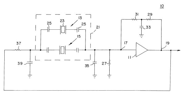
BXIEF DE~CRIPTION OF THE DR~WING
The sole Figure is a schematic diagram of a preferred
embodiment of the invention.
DESCRIPTION OF THE PREFERRED EMBODIMENT
Referring to the Figure an oscillator 10 constructed
in accordance with the principles of the invention includes an
amplifier 11 having resonant structures 13 and 15 coupled in
parallel between the input port 17 and output port 19 of the
amplifier 11. This parallel combination establishes a fault
tolerant resonator 21 which controls the oscillating frequency
of the system. The resonant structures 13, 15 may resonate at
the same frequency and each may include a crystal 23 and
isolation capacitors 25. The isolation capacitors may be
varied to tune the resonant structures for desired oscillator
operation. Though only two resonant structures are shown in
the Figure, it should be apparent to those skilled in the art
1~04794
2a 72558-15
that additional resonant structures may be added, should
qreater reliability be desired.
A resistor 27 is coupled to the input port 17. When
the amplifier is turned on, current flows through this resistor
to establish a bias required for linear amplifier operation.
RC circuit including series resistors 29, 31 and shunt
capacitor 33 coupled at the junction of the resistors 29, 31 is
included in the feedback circuit. Capacitor 33 is of
sufficiently large value to establish a very low impedance at
the oscillator freguency, thereby establishing resistor 29 as a
load on the amplifier and resistor 31 as a shunt across the
input resistor 27 during the oscillator operation. This
decouples the RC network from the feedback circuit during the
oscillator operation while providing negative DC feedback to
prevent oscillation when the fault tolerant resonator is
removed from the system.
~304'^~94
1 To establish the required 360 degree phase shift in the
feedback circuit, the resonator stage, c~nprising the fault
tolerant resonator 21 and the parallel circuit of resistors 27 and
31 with capacitor 35, must provide between 90 degrees and 180
degrees of phase shift. This phase shift is apportioned between
the fault tolerant resonator str~cture 21 and parallel RC circuit
27, 31, 35 to provide a compromise between between long term and
short term oscillator stability~ The closer the phase shift of
this resonator stage is to 90 degrees the smaller is the value of
the capacitor 35. This condition provides long term frequency
stability by decreasing the crystals drive level at the expense,
however, of decreasin~ the loaded "Q" of the circuit, thereby
degrading the short term frequency stability. When the phase
shift through the resonator stage is near 180 degrees, the
capacitance value of capacitor 35 is relatively large. This
condition increases the loaded "Q" of the circuit, providing an
increase in short te~n frequency stability at the expense of
increasing the drive level of the crystal, thereby adversely
affecting the long term frequency stability.
The phase shift difference between 360 degrees and that
provided by the amplifier 11 and resonator stage 21, 27, 31, 35
combination is aclde~ to the feedback circuit by the series
combination of resistor 37 and capacitor 39. me value of the
resi~tor 37 is detenmined by the output voltage of the amplifier
and the maximum AC current that may be drawn by the crystals and
amplifier. After this resistance value is determined, the
capacitance value of capacitor 39 is then chosen to provide the
added phase shift required.
Though the preferred embodiment utilizes a Pierce oscillator
configuration, those skilled in the art will recognize that the
technique may be applied to other oscillator circuits, as for
example Colpitts, Miller, Butler, and Hartley. It is to be
understood that the words which have been used are words of
description rather than limitation and that changes may be made
within thc purview of the appended claims without departing from
the true scope and spirit of the invention in its broader aspects.