Note: Descriptions are shown in the official language in which they were submitted.
13~211
PHA.21446 l 15-6-1989
A signsl generating circuit for ballast control of
discharge lamps.
This invention relates to a circuit for
generating signal voltages useful in the control of a
discharge lamp, and more particularly useful for
controlling the power to a high-pressure discharge
lamp operating as a headlight or fog lamp in a motor
vehicle or the lik~.
In USP 4,724,360, issued February 9, 1988,
there is disclosed a circuit for operating a high-
pressure discharge lamp (e.g. a high-pressure metal
to halide lamp) ~rom a source of DC voltage, such as an
automobile battery, by means of a direct voltage to
alternating voltage converter. The converter-ballast
circuit described therein is especially useful for
operating a headlight in an automobile or similar
vehicle which use~ a high-pressure discharge lamp as
the headlight.
In a ballast system of the general type
described in the aforeseid U.S. patent, it is necessary
to control the open circuit voltage in order to insure
that there is sufficient voltage available to produce
reliable lamp ignition. It is also required to control
the "run-up~ current (i.e. the current delivered to the
discharge lamp during the low arc voltage period that
occurs prior to the steady state or normal lamp operating
condition), and more importantly to control the steady
state lamp power.
In order to accomplish the control functions
mentioned above, it i8 useful to derive signals which
indiçate whether a load condition or an unloaded condition
is present, the open circuit voltage in the case of an
unloaded condition, the lamp voltage (for determining
~run-up" conditions), and the lamp power. It is also
130~i;~`1i
PHA.21446 2 15-6-1989
desirable to have the signals isolated from the discharge
lamp so that the lamp can "float" with respect to
ground for safety and EMI reasons.
It is therefore an object of the invention to
provide a circuit that produces isolated electric signals
which indicate open circuit voltage, lamp ignition,
lamp voltage and lamp power in an electronic ballast
in order to control the operation of the ballast and
lamp.
Another object of the invention is to provide
a simple and inexpensive circuit for generating the
required ballast control signals in an electronic
ballast of the type including a push-pull inverter
circuit and an inductive ballasting element.
S A further object of the invention is to
provide an electronic ballast for use with motor vehicle
headlights (discharge lamps) which can control lamp
power within a fairly narrow range despite substantial
variations in temperature, input voltage and lamp
voltage.
The above objects are achieved by means of a
simple signal generating circuit comprising three
transformers each of which has a secondary winding.
The secondary windings of the three transformers are
connected in series circuit and by means of the proper
turns ratios and winding polarities signals are produced
which provide all of the desired control information
to operate the ballast and lamp.
The first secondary winding is a secondary
winding of the ballast choke. In an open circuit
condition (lamp off) there is no voltage across this
winding, except for short duration ignition voltage
pulses which can be filtered out. When the ballast
3 circuit is loaded (lamp on) a voltage is present across
the first secondary winding which is proportional to
the ballast voltage. This signal voltage therefore
indicates a loaded or unloaded condition of the electronic
-13~ Z~
PHA.21446 3 15-6-1989
ballast.
The second secondary winding, which is connected
in series with the first secondary winding (ballast
choke winding), consists of a secondary winding on the
push-pull transformer of the ballast inverter circuit.
Since the lamp voltage is equal to the source voltage
(i.e. the output voltage appearing across the push-pull
transformer) minus the ballast choke voltage, the signal
voltage across the first and second series connected
secondary windings will be proportional to the lamp
voltage if the turns ratios are the same and the winding
polarities are correct.
In order to generate a signal which is appro-
ximately proportional to the lamp power, an approximation
technique is used whereby a signal voltage which is
proportional to the lamp (load) current is added to the
signal which is proportional to the lamp voltage.
The load current signal voltage is obtained by means of
the secondary winding of a third transformer which
has a primary winding connected across a small resistor
connected in the lamp current path, i.e. the resistor
i8 in series circuit with the lamp. The signal proport-
ional to lamp power is generated by adding together the
signal voltages proportional to lamp current and lamp
voltage.
In the case of a load which appears resistive,
power can be approximated over a limited voltage range
by summing the load current and voltage scaled by proper
constants. In order to provide satisfactory operation
of a high-pressure discharge lamp used as a motor
vehicle headlight, it is required to control the lamp
power within a range of 6% for a +2û% variation in the
lamp voltage. The circuit to be described provides an
error of only about 2% in the results of an adding
operation, K1V + K2I, versus the customary VI product
calculation of power, in the case of a 2û% variation
in lamp voltage.
130~Z~l
PHA.21446 4 15-6-1989
In an unloaded condition where the signal
voltages derived from the ballast choke and the lamp
current sensing resistor are each zero, a signal
proportional to the open cir~uit voltage can be sensed
either across the push-pull transformer winding alone
or across that winding in series with one or both of
the other two windings.
If a capacitor is used in series with the
ballast inductor, as in USP 4,724,360, it is possible
to take account of its effect on the circuit by changing
the ballast winding turns ratio by a factor XL/(X~-XC)
where XL is the reactive impedance of the ballast choke
and Xc is the reactive impedance of the capacitor,
assuming the lamp voltage and current waveforms are
approximately sinusoidal.
The invention will now be described in greater
detail by reference to the accompanying drawings in which:
Fig. 1 is a schematic circuit diagram illustrat-
ing a first embodiment of the invention,
Fig. la shows a modification of a part of the
circuit in Fig. 1,
Fig. 2 is a schematic circuit diagram illustrat-
ing a control circuit for use in the invention,
Fig. 3 is a schematic diagram of a second
embodiment of the invention, and
Fig. 4 is a schematic diagram of a third
embodiment of the invention.
Fig. 1 shows the basic combination of elements
for carrying out the invention. The system to be
described may be used to operate a low power (35W)
metal halide lamp 1 having an argon fill gas for use
as an automobile fog lamp. this type Qf lamp has an arc
voltage of 85`v ~20X and requires a voltage ignition
pulse of at least 1.5KV peak with a source voltage of
300V rms for reliable ignition of the lamp. The lamp
also needs a current of at least 1.25 amps rms immediately
after ignition in the case of a cold start and for an
130~
PHA.21446 5 15-6-1989
acceptably short "run-up" time.
In this system it is necessary to control the
open circuit voltage (for lamp ignition), the lamp
"run-up" current, i.e. the current delivered to the
discharge lamp during the low arc voltage period prior
to steady state lamp operation, and the steady state
lamp power.
In order to accomplish the foregoing it is
desirable to derive signals which indicate a loaded
or unloaded condition, the open circuit voltage in the
unloaded condition, lamp voltage (for determining run-up
conditions), and lamp power. It is also desirable to
have these signals electrically isolated from the lamp
so that the lamp can be floating with respect to ground
for safety reasons and to inhibit radiated EMI.
It is generally known that power can be
determined by taking the product of voltage and current.
The lamp power control in this system operates on the
assumption that lamp power over a limited range of lamp
voltage can be approximated by summing the lamp voltage
and lamp current modified by appropriate constants.
It can be shown that for a variable resistive load that
the relationship (1.4)(I) + (.005)(V) = 1 provides a
maximum error of about +2% when compared with a constant
35W over the voltage range from BOV to 12ûV. Similar
levels of error have been found for lamp loads.
A signal proportional to (1.4)(I) + (.û05)(V),
i.e. lamp power, is generated by using the secondary
windings on the oscillator transformer and ballast
choke for the lamp voltage signal and a sense resistor
and transformer for the current signal. The various
windings are connected in series to produce the desired
"power" signal.
36 In Fig. 1, a DC/AC inverter 2 is connected to
a source of ~C supply voltage, e.g. an automobile battery,
via input terminals at DC. The inverter supplies a
sinusoidal AC signal to a primary winding 3 of an output
1305Zil
PHA.21446 6 15-6-1989
transformer 4 having a first secondary winding 5 for
supplying AC power to the lamp load. The DC/AC inverter
could be of several types, ànd could have a transformer
coupled output or a simple inductor coupling. A sine
5 wave inverter is preferable. The power delivered by the
inverter is controlled via a DC control input terminal 6.
The ballast is controlled by controlling the DC input
to the DC/AC inverter by means of a controlled DC/DC
stage. This stage may be a boost converter, but coold
also be of another type.
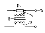
The AC voltage induced in winding 5 is supplied
to the discharge lamp 1 via a series circuit consisting
of a ballast coil 7, which is the primary winding of a
transformer 8 having a secondary winding 9 having one
end connected to ground, a DC blocking capacitor 10 and
a lamp current sensing resistor 11. The capacitor 10
in series with the inductor 8 is optional, its function
being to prevent lamp rectification. The effect of the
capacitor 10 on the control voltage developed at terminal
15 can be taken into account by a judicious choice of
the winding turns ratio of ballast transformer B.
A primary winding 12 of a current sensing
transformer 13 is connected in parallel with the current
sensing resistor 11. The transformer 13 has a secondary
winding 14 connected to an output control terminal 15
at which a voltage Vc appears. The voltage Vc relative
to ground i8 indicative of lamp power. Alternatively,
lamp current may be sensed by means of the modified
circuit shown in Fig. la where the resistor 11 is
connected in parallel with the secondary winding 14 of
transformer 1J, rather than in parallel with the primary
winding 12, as in Fig.l. This configuration has the
advantage that the "sense" resistor 11 now has a higher
3 resistance value. This type of resistor is more readily
available.
The inverter output transformer 4 has a further
secondary winding 16 connected in series circuit with the
13QS~
PHA.21446 7 15-6-1989
secondary windings 9 and 14 between ground and output
control terminal 15.
In the open circuit condition, i.e. before
ignition of the discharge lamp, no voltage is induced
5 in secondary winding 9 (except for short duration ignition
pulses) since there is no current flow in the primary
winding 7. When the circuit is loaded, i.e. the lamp is
in its operating s-a~e, a voltage is produced across
winding 9 which is proportional to the ballast voltage.
This signal voltage, VA, at terminal 17 provides an
indication as to the load condition, i.e. whether the
lamp is on or off.
A voltage proportional to the source voltage is
induced in the secondary winding 16 of the inverter
output transformer 4. Since the lamp voltage is equal
to the source voltage minus the ballast inductor voltage,
the voltage develpped across the series combination of
the two secondary windings 9 and 16 will be proportional
to the lamp voltage, assuming the turns ratios are the
20 same and the winding polarities are correct. The winding
polarities are indicated by the conventional dot symbols
on the transformer windings.
In the operating condition of the lamp, the
lamp current flows through resistor 11 to produce a
25 voltage drop proportional to lamp current. Transformer
13 induces a signal voltage in the secondary winding
14 that is proportional to lamp current. Since the
voltage developed across the series connected windings
9 and 16, i.e. the voltage between ground and terminal
30 18 is proportional to lamp voltage, and the voltage
across series winding 14 is proportional to lamp current,
the voltage appearing across all three serias-connected
winding, g, 16 and 14, i.e. from ground to terminal 15,
is approximately proportional to lamp power, given the
~5 assumptions described above. Thus, a signal voltage is
generated at terminal 15 which is approximately proport-
ional to lamp power by virtue of the addition of a signal
'
13(~5~il
PHA.21446 8 15-6-1989
voltage proportional to lamp voltage (windings 9, 16)
and a signal voltage proportional to lamp current
(winding 14).
IN the unloaded condition (lamp off) the
5 voltages developed by ballast inductor 7 and current
sensing resistor 11 are both zero so that a signal
indicative of the open circuit condition can be sensed
across either winding 9 or 14. The level of the open
circuit voltage can be obtained from the voltage across
winding 16 or, since the voltages across windings 9 & 14
are nearly zero, across the series combination of
wwindings 16 & 9, or 16 & 14 or across all three windings
in series. Thus, a voltage VA at terminal 17 can provide
an indication of a loaded or unloaded condition, a
voltage VB at terminal 18 indicates the value of lamp
voltage and a voltage Vc at terminal 15 indicates lamp
power.
Fig. 2 is a schematic diagram of the control
circuits which are responsive to the control signals
developed at terminals 15, 17 and 18 in the circuit
of Fig. 1 in order to provide the control functions
for the ballast and lamp. A control signal at output
control terminal 6 is coupled to the control input
terminal 6 of the DC/AC inverter 2 of Fig. 1.
During steady-state operation of the lamp,
the signal Vc at terminal 15 provides an indication of
lamp power. The circuit consisting of amplifiers 19, 20,
resistors 21-25 and diodes 26,27 form a precision
variable gain active rectifier circuit producing at
the output of amplifier 19 a full-wave rectified version
of the input signal (K1V + K2I) at input terminal 15.
The output signal of amplifier 19 can be filtered using
a long time constant (e.g. approximately 100 ms). the
3 resistor 25 is preferably a variable resistor by means
of which the lamp power can be manually adjusted by
adjusting the gain of the active rectifier circuit.
The gain of the active rectifier stage is
130S~l~
PHA.21446 9 15-6-1989
equal to R5/R6 where R5 is the resistance of resistor
24 and R6 is the resistance of resistor 25, and where
R5 = R4 = ~3 = R2, where R4, R3 and R2 are the resistance
values of resistors 23, 22 and 21, respectively.
A Zener diode 28 protects the input circuit of
amplifier 20 against any overvoltage. The full wave
rectified output of amplifier 19 is filtered by means of
resistor 29 and capacitor 30 connected in series
between the output of the amplifier and ground. A DC
control signal indicative of the lamp power level is
thereby produced at the non-inverting (+) input of an
output error amplifier 31. The control signal at
terminal 46 is negative in the circuit described.
However, if the circuit was modified to produce a positive
control signal, then terminal 46 would be connected to
the inverting (-) input of amplifier 31.
The inverting input (-) of amplifier 20 is
connected to input terminal 15 via the variable resistor
25 and to its output via a series circuit of resistor
23 and diode 26. The non-inverting input of amplifier 20
i8 connected to ground. The inverting input of amplifier
19 i8 connected to the junction of resistor 23 and diode
26 via a resistor 22, and is also connected to its
output via a feedback resistor 21. The non-inverting
input of amplifier 19 is connected to the output of
amplifier 20 via a diode 27 and to the inverting input
(-) of amplifier 20 via resistor 24.
Although various known circuits could be used
to implement the DC/AC inverter 2 (Fig. 1), a preferred
apparatus consists of an up-converter preconditioner
satge followed by a self-oscillating current-fed sinus-
oidal push-pull inverter. The current (power) delivered
to the lamp is determined by a DC control voltage at the
input of the push-pull inverter since the push-pull
oscillator functions as an AC voltage source at the
secondary winding 5 of output transformer 4 (Fig. 1).
The AC voltage in secondary winding 5 is proportional
1305211
PHA.21446 10 15-6-1989
to the DC input. The ballast element 7 then regulates
current as a function of the AC voltage source.
Lamp current is controlled by controlling the DC voltage
in the up-converter stage of the DC/AC inverter 2.
During the low arc voltage lamp run-up phase,
it is necessary to control the lamp current to provide
an adequate run-up current. The relatiosnhip 1.4 I +
.005V = 1 provides only about 640 ma of current at a
low arc voltage of 20 volts, whereas 1.1 amps or more is
required. It is therefore necessary to modify the gain
of the active rectifier/filter stage to provide the
necessary current at low arc voltages. THis is accomplished
by the lamp voltage monitoring circuit connected to input
terminal 18. Terminal 18 receives the lamp voltage
signal VB from terminal 18 of the circuit of Fig. 1.
Input terminal 18 is coupled to the non-
inverting input of amplifier 32 via a series connected
diode 33 and a resistor 34. The non-inverting input is
connected to an output junction point 35 via the parallel
circuit of capacitor 36, resistor 37 and Zener diode 38
connected in series with diode 39. The junction point
of elements 36-39 is connected to ground. A reference
voltage at terminal 40 is applied to the inverting
input of comparator 32 via a variable resistor 41.
A feedback resistor 42 connects the inverting input
to the output, which in turn is connected to junction
35 via a resistor 43.
The output junction 35 is connected via a
resistor 44 in series with a diode 45 to a common input
junction point 46 for the error amplifier 31.
The lamp voltage signal at terminal 13 is peak
detected by diode 33 and capacitor 36. The resistor 34
and the Zener diode 38 protect the input of comparator
amplifier 32 from voltage transients. The gain of the
rectifier-filter stage is modified during the run-up
phase by controlling the gain of amplifier 32 by means
of resistors 41 and 42. Thus, the lamp voltage is
~3~
PHA.21446 11 15-6-1989
monitored and subtracted from the filtered output signal
of the active rectifier stage when the lamp voltage
drops below a predetermined level set by variable
resistor 41.
When the lamp voltage is below the set point
level the K term in the power expression K (1.4 I + .005V)
= 1 is changed as a function of voltage, which has the
effect of changing the slope of this expression whenever
the lamp voltage is below the adjusted set point voltage.
The slope is adjustable by adjusting the gain of the
amplifier monitoring the lamp voltage. The maximum
amount of attenuation is determined by rssistor 44 and
can be adjusted by making this resistor variable.
If resistor 44 is variable, it can be used to adjust
the run-up current during the low arc voltage phase
of the lamp (lamp start-up).
In the open circuit condition (lamp off),
the signal voltage at terminal 15 represents the open
circuit voltage. During open circuit it is necessary to
modify the power control loop because when the lamp
current is zero, the power control loop will produce
an open circuit voltage of approximately 170 volts rms,
whereas a voltage greater than 300 volts rms is necessary
at this time. It is therefore necessary to modify the
loop gain in the open circuit condition so as to produce
the desired 300 V rms.
The circuit for monitoring the open circuit
condition i8 connected to input terminal 17 which
receives the voltage VA indicative of the ballast coil
voltage. In the case of an open circuit, the voltage VA
at terminal 17 is nearly zero, except for short duration
ignition pulses.
The terminal 17 is connected to the non-
inverting input of comparator amplifier 47 via a series
circuit consisting of a diode 48, a first resistor 49
and a second resistor 50. A reference voltage at terminal
51 is applied to the inverting input of amplifier 47.
.. . .
13(~
PHA.21446 12 15-6-1989
The non-inverting input is coupled via the parallel
circuit of capacitor 52 and resistor 53 in series with
a Zener diode 54 to the junction between resistors
49 and 5û. The junction point of ele~ents 52-54 is
connected to ground. The output of comparator 47 is
connected to input junction 46 via the series circuit
of diode 55 and resistor 56.
The ignition pulses at terminal 17 are clipped
by resistor 49 and Zener diode 54 and the signal voltage
lo at this terminal is rectified by diode 48 and is filtered
by resistors 50, 53 and capacitor 52 to produce a DC
signal at the non-inverting (~) input of amplifier 47.
This ~C signal represents the ballast coil voltage.
In the open circuit condition, the DC signal
is lower than the reference voltage at terminal 51,
thus producing a low output voltage for comparator
amplifier 47. This is operative to attenuate the signal
at the common input junction 46, thus effectively
decreasing the gain between the input terminal 15 and
the signal input of error amplifier 31. By a proper
choice of resistor 56 the open circuit voltage can be
controlled to a value of 300 V rms.
In the loaded condition (lamp on), the signal
voltage across capacitor 52 is greater than the reference
voltage at terminal S1 which causes the output voltage
of amplifier 47 to go high, thereby reverse biasing
diode 55 and isolating the open circuit monitor from the
error amplifier 31. In fact, during steady-state
operation of the lamp, the outputs of amplifiers 32 and
47 are both high so that respective diodes 45 and 55
are both revarse biased to keep amplifiers 32 and 47 from
influencing the operation of the control circuit.
In the case of the open circuit voltage
there is a "step" response in the change of gain of the
rectifier/filter stage. In the circuit for gain mo~ifi-
cation in the run-up phase the gain is varied to provide
a smooth transition so that there will not be a visible
13U~2i~L
PHA.21446 13 15-6-1989
step in the light output of the lamp when the transition
occurs.
The full wave rectified output of amplifier
19 is filtered by resistor 29 and capacitor 30 to produce
a DC signal indicative of the level of lamp power.
This signal is compared in error amplifier 31 with a
DC reference voltage at terminal 57. The resultant error
signal at terminal 6 is then used as a control signal
to control the output of the DC~AC inverter. If lamp
power is too low, the error signal increases the DC
control voltage and hence the lamp power is increased.
If lamp power is too high, the opposite occurs. The
error amplifier is compensated to ensure loop stability.
Fig. 3 shows a second embodiment of the
invention which is a modification of the circuit shown
in Fig. 1. The circuit of Fig. 3 uses a simple inductor
71 instead of a transformer at the AC output as in Fig.
1. Energy is supplied from a DC/DC inverter 61 via the
inductor 60 to a resonant inverter 62. This current-
fed push-pull circuit provides the same signal voltages
at terminals 15, 17 and 18 as the circuit of Fig. 1
and operates in a similar manner in the development
of these signal voltages.
Fig. 4 shows a further modification of the
circuit of Fig. 1 whihc now uses a leakage transformer
63 for coupling a DC/AC or AC/AC inverter 64 to the
discharge lamp 1. In this apparatus a signal voltage
is developed at terminal 65 which is indicative of the
lamp voltage since the sense winding 66 is tightly
coupled to the secondary winding of leakage transformer
63. Lamp current is sensed in the same way as in Fig. 1.
A signal voltage is developed at terminal 67, relative
to ground, which is approximately proportional to lamp
3 power. The signal voltage appearing between terminals
65 and 67 can be used to provide an indication of the
lamp load condition, i.e. whether the lamp is on or off.
130S~l
PHA.21446 14 15-6-1989
The signal voltages developed at terminals
65 and 67 are applied to the inputs of a control device
68 which will function similar to the control circuit
of Fig. 2 to derive a control signal at the output 69.
5 This control signal is coupled to a control input of
the inverter 64 so as to control lamp current or power.
The inverter may control the lamp curent by means of
amplitude control of the primary.
A further capacitor 70 may be connected across
the series connection of capacitor 10 and lamp 1, as
indicated in broken lines. The capacitor 70 is optional
and it functions to modify the waveform of the lamp
current, i.e. to give it a more sinusoidal waveshape.
The capacitor 70 is also designed to resonate with the
leakage inductance of transformer 63 in order to
generate a high voltage for ignition of the discharge
lamp.
Although the invention has been described in
connection with particular useful embodiments thereof,
it will be apparent that various modifications can be
made without departing from the spirit and scope of the
invention.