Note: Descriptions are shown in the official language in which they were submitted.
~3~533~
This invention generally relates to photometric
devices for performing densitometric measurements on
translucent sites. More particularly, this invention
relates to an au~omatic scanning device using end-
point and/or kinetic measurement techniques for
measuring the optical density of a plurality of
translucent samples in order to analyze their
content~.
A variety of techniques and devices are
commercially available for the detection and
measurement of substances present in fluid or other
translucent samples by determining the light
transmitivity of the sample. In particular, a number
of photometric devices are capable of simultaneously
performing individual assays on a plurality of liquid
or other translucent samples. Such methods generally
handle a multiplicity of samples by using
"microplates" which contain a standard array (8 x 12)
of wells and which are made of an optically
-- 1 --
~ 27-130/hay
.
~36)~34
transparent material. The optical density of the
samples is measured by determining attenuation
undergone by light as it passes through the
translucent samples, contained in the microplate
wells, to conventional photodetecting means.
A widespread use for microplates is in the
enzyme-linked immunosorbent assay IELISA) technique
which is used for detection and quantitation of an
extensive range of substances and biological cells in
academic research and biotechnology as well as for
clinical testing. In such assays, molecules of a
marker enzyme (such as alkaline phosphatase) are
deposited on the bottom and part of the way up the
sides of each of the wells of a microplate; each well
having been assigned to interact previously, directly
or indirectly, with a sample containing an analyte of
interest. The number of marker enzyme molecules
bound to each well of the plate is a function of the
concentration of analyte in the sample of interest.
Determination of the activity of the bound enzyme,
therefore, permits detection or quantitation of the
analyte.
For determination of fluid-phase enzyme
activity, current techniques for both research and
clinical applications employ kinetic analysis which
involves measurement of the initial rate of enzyme- ~ -
catalyzed, chromogenic reactions in the presence of
excess of the enzyme substrate; a procedure which~has
several well-known advantages over the alternative
"end-point" analysis method of allowing the enzyme to
react with a chromogenic substrate for a fixed period
of time and then making a single optical density
measurement after quenching the enzymes. In kinetic
analysis, multiple readings are made within the
initial (typically linear) reaction period and the
27-130/hay
3L3~3~
intervals between readings are necessarily short
(typically less than 30 seconds). By using kinetic
analysis, the introduction o errors caused by
~a) differences in initial optical density and/or
~b) loss of independence from substrate
concentration, is substantially avoided.
Currently available automated optical density
measurement instruments for microplates typically
function by mechanically moving either the multi-well
microplate or the optical components themselves in
order to successively perform assays of samples
located at the plurality of individual assay sites.
This requirement places a severe restraint on the
time required to actually measure the transmittance
in all wells of the microplate, thereby making large
scale kinetic analysis assay applications impractical
due to the extended sampling times. In part because
of this, "end-point" analysis is employed for ELISA
protocols read by current instruments.
A measurement system which is capable of reading
a plurality of assay sites in sequence without
relative physical movement of the microplate and the
optical components is disclosed in Wertz et al. U.S.
Patent No. 4,408,534 which discloses the use of fiber
optic transmission means with a single light source
sequentially coupled to a plurality of optical fibers
which transmit li~ht to the measurement sites.
However, the apparatus described in the Wertz-patent --
uses a highly inefficient system for coupling light
from the light source into the optical fibers, which
in turn leads to a variety of potential problems for
kinetic measurements of enzyme activity. For
example, the Wertz apparatus requires a high power
light source and the increased light intensity can
adversely affect the chemical reactions in the assay
27-130/hay
~3~ ~
sites by increasing the operating temperature of the
measurement system non-homogeneously and hence
altering the rates of reaction in different wells to
a different extent. In addition, such systems are
unduly complex because of the wide fluctuation in
signal levels generated as a result of the reception
of light at the photodetectors after it has passed
through the sample sites; this prevents efficient
utilization of the overall dynamic range of
amplification for the signal amplifiers of the
measurement system.
Another limitation of conventional microplate
reading devices is their inability to make useful
quantitative measurements for ELISA protocols
performed in filter-bottom microplates. A principal
problem is that the individual wells in such plates
vary considerably in their initial optical density
relative to alr thereby introducing considerable
error when end-point measurements are taken. Kinetic
analysis, on the other hand, is not affected by this
type of problem.
Another major problem associated with
conventional microplate reading devices, when used
for assayin~ chromogenic reactions kinetically, is
that they are subject to errors arising from erratic
redistribution of the colored product as a result of
phase separation and/or uncontrolled bulk movement of
the aqueous phase of the sample during kinetic ~ -~
analysis. More specifically, in the case of ELISA
protocols, where the enzyme is bound to the plastic
surface of the microplate wells (on the bottom and/or
part way up the sides), the bound enzyme interacts
with an unstirred aqueous phase layer which typically
causes localized phase separation of the colored
product of the enzyme reaction due to its high local
27-130/hay
~3~ 4
concentration. This separation introduces an
unquantifiable error and a degree of non-linearity
into such kinetic measurements. Even in cases where
the colored product remains in true solution, erratic
bulk movement of the aqueous phase leads to uneven
redistribution of the concentrated product and hence
to an unquantifiable error.
It is a primary object of this invention to
provide an automatic photometric device for multi-
site kinetic and/or end-point densitometric assays,
which is capable of accurately acquiring a large
number of measurements in a relatively short period
of time.
Another important object of this invention is to
provide such a photometric measurement device which
uses a single relatively low power light source
leading to reduced ambient operating temperature and
extended life.
Another object is to provide such a photometric
device with convenient control over the accuracy with
which the sensed signals for this measurement system
are processed.
It is a related object of this invention to
provide a photometric device of the above kind which
does not re~uire relative mechanical movement of the
microplate and the optical components of the system
in order to perform successive multi-site assays.
Another important object of this invention is to
provide such a photometric device which, by virtue of
its ability to perform kinetic analysis, is able to
make quantitative measurements of enzyme activity in
filter-bottom microplates.
27-130/hay
13~3;~L
Another 1mpor-tant object of this invention is to
provide such a photometric device which provides
signlficantly enhanced ~olor distribution in the assay of
chromogenic reactions and lS not subject to measurement
errors arising from nonuniform distribution of -the colored
product in such chemical reactions.
It is also a related object of this invention to
provide a measurement device of the above kind which iæ
efficient, economical and convenient to use.
These and other objects are achieved according to the
system of this inven-tion by providing a photometric kine-tic
measurement device for analyzing samples contained in a
plurality of sample sites disposed on a multi-site assay
plate, the device comprising: a ligh-t source for providing
light to one or more of said sample sites; photodetector
means for receiving light transmitted -through each of said
one or more sample sites and for providing a signal in
response to said light received wherein the ligh-t vertically
passes through the sample; means for imparting oscillatory
movement to said multi-site assay plate for a pre-determined
time before each of a series of readings is performed on a
sample site in order to agitate the sample therein; and a
means for kinetic analysis of the signal of the
photodetector means.
The present invention also provides a multibeam
photometric measurement device for measuring optical density
of samples contained in a plurality of sample sites disposed
on a multi-site assay plate, said device comprising: a
single light source adapted through coupling means to be
selectively applied, according to a predetermined sequence,
through selected ones of a plurality of light transmitting
means to selected ones of said samples sites; a plurality of
photodetector means disposed on a detector board and
positioned in relation -to said assay plate in such a way
that light transmitted through each of said sites is
received by a corresponding photodetector; means for
simultaneously imparting mixing movement to said samples
~'A..'~
~omprlsing rneans for impar-tincl movenlent to sald assay plate
for a predet.ermined time before a reading is performed on a
sample site; and means fo:r analyzing the output of said
photodetector means to de-termine and indicate the optical
density of sai.d sites.
The present inven~ion also provides a photometric
measurement device for measurincl optical density of samples
con-tained in a plurality of sample sites disposed on a
multi-site assay plate, saicl device comprising; a ligh-t
source for applying light to selected ones of said sample
sites; photodetector means posi-tioned in relation to said
assay pla-te in such a way that light -transmitted through
each of said sites is received by said photodetector; means
for simultaneously imparting mixing movement to said samples
comprising means for i.mparting movement to said assay plate
for a predetermined time before a reading is performed on a
sample site; and means for analyzincl the OUtpllt of said
photodetector means to determine and indicate the optical
density of said sites, said means for analyzing comprising:
means for sequentially selecting the analog output signals
for desired photodetectors for analysis; means for
converting said analog signals to thei.r corresponding
digital values; means for amplifying said analog signals in
such a way as to utilize a substantial portion of the
dynamic range of said analog -to digital conversion means;
means for storing precalculated values corresponding to said
digitized values, acceptirlcl saicl d:ig:it:ized vallles and
retrieving the corresponding stored precalculated value in
response to each of sa.id digi-tal value~; and means for
processing said retrieved values in order to calculate the
optical density of said samples.
The present invention also provides a Pho-tometric
measuremen-t device for measuring optical density of samples
contained in a plurality of sample sites disposed on a
multi-site assay plate, said device comprising: a light
source for applying light to selected ones of said sample
site.s; photodetector means positioned in relation to said
assay plate in such a way tha-t ligh-t transmitted -through
-- 7
each of Sdl~ SlteS lS received by said photocletector, means
for slmultaneouslv i.mpartl.ng mixlng movement to sald ~amples
comprislng means for lmparting movement to said assay p]ate
for a predetermined time be:Eore a reading is performed on a
sample s:ite; and means for analyzing the output of said
photodetector means to determine and indicate the optical
densi-ty of said si-tes, wherein said photodetectors are
divided into blocks, each consisting of a plurality of
photodetectors, in such a way that photodetec-tors in said
blocks are spaced substantially apart on said detector
board, and the outputs of the photodetectors of each said
block are connected together to yield a common output
signal, whereby the output of a selected photodetector can
be analyzed by selecting -the common output signal for the
block in which the photodetector lies.
In a further aspec-t, the present invention provicles a
method for measuring the transmittance of a plurality of
sample sites on a mul.ti-site assay plate comprising the
steps of selectively focusing light from a single light
source through a pl.urality of light tran.smitting means upon
selected ones of said sample sit.es, for each sample site,
measuring , at. a succession of time in-tervals, the intensity
of light passing through the reacting sample in the sample
site by using pho-todetecti.ng means, oscillating said assay
plate for a first fixecl time durati.on in order to agi.tat.e
the samples contained therein and allowing the agi.tated
samples to settle for a second fixed time duration before
performing each of said successive measurements, measuring
the intensity of light when coupled directly from said light
transmitting means to said pho-todetecting means, measuring
the intensity of light when coupled from said light
t.ransmi.tting means to said photodetecting means, through the
sample site when it ~ontains no reacting sample, using said
measurements to calculate the optical density of said sample
sites.
In a further aspect, the present invention provides a
method for taking measurements of the transmi.ttance of a
plurality of sample sites on a multi-site assay support,
- 7a -
c~omplislr1q the steps of measllrlnci the photosigna.l generatedhy llght shininq through an airspace in the absence of a
samp.le to ~ive a flrst air t.ransmission photoslgnal value;
measuring the photosignal generat.ed by light shining through
an ai:rspa~e in the ahsence of said support to give a second
air transmission photosignal value, adjusting sai.cl
relationship to compensate for a difference between said
first air photosignal value and said second air photosiynal
value.
In a still further aspect, the present invention
provides a method for determining a colormetric assay
utilizing a multibeam photometer having a photodetector
means positioned in relation to a multi-site solid such that
light is received at a plurality of different sites on the
surface of sai.d photodetector means, said me-thod comprising
the following steps:
measuring the photosignal generated by light shining
through an airspace in the absence of a sample support -to
give a first air transmission photosignal value; measuring
the photosignal generated by light shining through an
airspace in the absence of said suppor-t to gi.ve a second air
transmission photosignal value; adjusting said relationship
to compensate for a difference between said first air
photosignal value and said second air photosignal value.
In a fur1,her aspect., the present inven-tion provides a
method for measuring the t,ransmi.ttance o.E a plllrcllitY of
samples conta:Lned in a pl.urality o.E sample sites on a multi-
si-te assay ~late wh:Lle sai,d assay plate is in a device for
carrying our said measuring, said method comprising the
steps of:
inserting said assay plate into said device; imparting
mi~ing movement to said samples by imparting movement to
said assay plate for a first fixed time dura-tion; providing
light to one or more of said sample sites; for each sample
si-te, measuring the intensity of light passing through the
sample in the sample site; and removing said assay plate
from sai.d device.
- 7b -
~;313S3~
Other objects, characteristics dnd acl.vanta~les of the
present invent:i.on wl.ll be apparent from the followin~
detalled clescrl~lion taken in conjunction with the
aecompanyi.nq drawi.ng.s, in whieh:
Fig. I :LS a simplified schematic representa-tion of a
photometrie reading device accordlng to the system of this
invention;
Fig. 2 is an illustrati.on of the fiver distributor
showing the varlous designated posi-tions utilized to eouple
the light souree to eaeh of the plurality of optie fibers;
Fig. 3 is an illus-tration of the disposition of the
various optieal fibers wi.thin a fiber manifold assoeiated
with the ample assay sites;
Fig. 4 is a simplified block cliagram of the proeessing
eireuitry aceording to -this invention;
Fig. 5 is a flow eha:rt representing the general
sequenee of operations involved in a typieal sequential sean
of the sample plate aeeording to the illustrative
measurement syst.em;
Fig. 6 is a flow diagram of the operating sequenee
undergone by the system as part of the air eali.bration
phase;
Fig. 7 is a flow ehart representing the sequenee of
operations involved in performing the read phase on a sample
tray.
f~
533~
FIG. 8 is a perspective view of a preferred
embodiment of a multibeam photometer according to the
present invention;
FIG. 9 is a side elevation cutaway view of a
microplate well inserted between the LED array and
photodetector of the photometer of FIG. 8;
FIG. 10 is a block diagram of the electronic
control circuitry for the photometer of FIG. ~;
FIGS. llA and llB are circuit diagrams of a
portion of the control circuitry of FIG. 10;
FIG. 12 is a timing diagram for portions of the
circuit of FIGS. llA and llB; and
~ IG. 13 is a flow chart of a computer program
for controlling the control circuit of FIG. 10.
While the invention will be described in
connection with certain preferred embodiments, it
will be understood that it is not intended to limit
the invention to these particular embodiments. On
the contrary, it is intended to cover all
alternatives, modifications and equivalent
arrangements as may be included within the spirit and
scope of the invention as defined by the appended
claims.
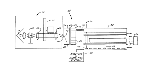
Referring now to the drawings, FIG. 1 is a
simplified schematic representation of an exemplary
kinetic measurement system 10 embodying the present
invention. The system l0 includes a light
assembly 12 capable of providing a finely focused
reflected beam of light for coupling to the test or
assay sites. The light assembly 12 comprises a
single source of uniform, reflected and focused light
14 which, in the preferred embodiment, includes a
27-130/hay
~3~ 3~
tungsten-quartz bulb emitting light in a wavelength
range of about 300 to 900 nanometers. The output of
the light source 14 is passed through a chopper 16
which modulates the light at a fixed frequency which
in the preferred embodiment is 800 hertz.
The modulated light from the chopper 16 is
collimated through a lens 18 onto a filter wheel 19
which extracts light of a selected wavelength and
bandwidth which corresponds to the wavelength at
which the test samples exhibit light absorbency. The
filtered light is passed through a lens 20 which
receives the collimated light and focuses it onto a
l precise point 22 from which the light can be coupled
to selected fibers which conduct the light to the
plurality of assay sites.
The kinetic measurement system 10 utili~es a
highly efficient and structurally simple light
coupling and transmitting mechanism. As shown in
FIG. 1, the collimated light exiting the light
assembly 12 is directed to a light coupling
arrangement which includes a cylindrical rotor 24
which is capable of being rotatably positioned
accurately about its axis. The rotor 24 includes an
optical fiber 26 having an input end 28 located at
the center Gf the rotor 24 and coincident with the
focal point 22 of the light output from the light
assembly 12. The output end 30 of the fiber 26 is
located near the periphery of the fiber rotor 24 so =~
that as the rotor rotates the input end 28 of the - --
fiber remains stationary with respect to the light --
assembly 12 while the output end 30 moves around a
circular path. The rotor 24 thus permits efficient
coupling of light from the light assembly 12 into
selected ones of a plurality of light transmitting
means which carry the light to corresponding assay
sites.
-- 10 --
27-130/hay
~3~353~4
The light output from the fiber 26 in the
rotor 24 is received by a iber optic distributor 32
containing a multiplicity of optical fibers 34 having
their input ends arranged in a circular array. This
circular array of fiber ends has the same radius as
the location of the output end of the fiber 26 in the
rotor 24 so that as the rotor 2g is indexed about its
axis, the output end of the fiber 26 is brought into
alignment with successive fibers 34 in the
distributor 32. On the output side of the
distributor 32, the fibers 34 are brought together to
form a fiber bundle 36 which leads to a fiber
i manifold 38 which aligns each of the fibers 34 with
one of the assay sites (to be described below).
The rotor 24 is indexed by means of a suitable
stepper drive or other appropriate controllable
displacement means so that it sequentially directs
the collimated light from the focal point 22 into
different fibers 34 of the bundle 36.
The use of the optical fiber coupling
arrangement to couple light from the light
assembly 12 to individual optical fibers 34 within
the distributor 32 constitutes a significant
advantage because of the efficiency of transmission
associated with the mechanism. More specifically,
the optical fiber 26 ensures that substantially all
the collimated light from the light source 14 is
coupled into a selected optical fiber 34 without any -
significant diffusion at the point of coupling at -
either end of the coupling fiber 26. Thus, light
from the source 14 is coupled through the rotor 24
only into a selected one of the optical fibers 34
with minimal undesired coupling of light into optical
fibers adjacent to the selected fiber. This highly
efficient coupling allows the use of a single light
27-130/hay
5 3 ~! 41~
source with relatively low power capacity since a
high percentage of light emanating from the source is
transmitted to the site of measurement.
The illustrated light source in FIG. l is a
convenient and preferred form; however any light
source or a plurality of light sources providing
light of equal intensity and having the desired range
of wavelength can be used. In this regard, an
alternative form of photometric measurement, which is
based upon a sequentially operated multibeam light
source, will be described in detail below in
connection with FIGS. 8-13.
At the site of measurement, light emanating from
any of the optical fibers 34 located within the fiber
manifold 38 is directed to a corresponding assay site
on a sample plate 40 through an array of lenses 42
disposed between the manifold 38 and the sample plate
40. The sample plate 40 may be a conventional
microplate having a series of wells, usually an array
of 96 wells arranged in 8 rows having 12 wells
each. The sample plate is preferably mounted in an
area where the ambient temperature is regulated,
e.g., by means of a fan, so as to present isothermal
conditions about the sample plate. This is important
in minimizing inaccuracies from varying rates of
reaction occurring at different sample sites as a
result of a temperature gradient about the sample
plate. ~
An array of photodetectors 44 is provided on a
detector board 46 in the form of a matrix conforming
to the positions of the wells located on the sample
plate 40. A second lens array 48 is positioned
beneath the sample tray 40 and serves as means for
focusing light from each well of the sample plate 40,
after the light has passed through the well. The
- 12 -
27-130/hay
3;~
lens arrays 42 and 48 are of the conventional type
and include apertures (not shown) which function to
direct the light towards the individual lenses and
minimize diffusion of light into adjoinino lenses.
The sample plate 40, or at least the bottom of each
well in the sample plate, is translucent or
transparent so that light coupled to a particular
optical fiber within the fiber manifold 38 and then
collimated onto a corresponding sample well
penetrates the well and its contents, passes through
the corresponding focusing lens disposed within the
lens array 48, and reaches the corresponding photo-
i cell 44 located immediately below the sample well.
The photodetector 44 senses the intensity of thelight passing through the corresponding sample well
and produces an electrical output signal proportional
to the intensity of light incident on its surface.
Each of the photodetectors 44 provided on the
detector board 46 functions in a similar manner and
provides a signal which is proportional to the
varying intensity of the light impinging thereon.
This varyiny intensity is caused by the varying
transmittance offered by the sample as a chemical
reaction progresses therein and alters its
constituency. The resulting electrical signals from
the photodetectors 44 are fed to an analysis and
indication system 50 which processes the received
signals and provides an external indication of the
transmittance or optical density of each of the
samples contained within the multiple wells of the
sample plate 40.
The measurement system of Fig. 1 also includes a
single reference optical fiber 52 positioned adjacent
to the focal point 22 so that the fiber 52 receives
light continuously whenever the light source 14 is
27-130/hay
3;~
energized, i.e., whenever any of the sample sites is
being tested. The light emanating from the output
end of the reference fiber 52 is coupled through air
or an empty sample well to a separate
photodetector 45 on the detector board 46, and
provides a reference photode~ector signal whose
significance will be described in detail below.
The optic fiber distributor 32 also has an
optical fiber designated as the "home" fiber which
serves as a reference for determining the current
position of the distributor 32 relative to the
coupling rotor 24. The function of the home fiber
will also be described in more detail below.
In order to promote uniform distribution of the
color resulting from chromogenic reactions in the
samples being measured, the measurement system of
FIG. l is provided with means for agitating the
chemical solutions contained within the plurality of
wells of the sample plate 40. More specifically, as
shown in FIG. l, the sample plate 40 is attached to
an agitating mechanism 54 which oscillates the tray
in a manner that brings about a thorough mixing of
the chemical solutions contained within the sample
wells.
A common problem with conventional microplate
readers, if used for kinetic analysis of ELISA, is
that distribution of the color produced as a
chromogenic reaction progresses may be uneven across
the width of a sample well. Since kinetic optical
density measurements generally involve the
transmission of light through the central portion of
a sample well, uneven distribution of color (e.g.,
due to color development on the walls or corners of a
sample well) can severely distort the accuracy of the
transmittance readings. Non-homogeneous distribution
- 14 -
27-130/hay
~3C~
of color in the samples can also produce significant
variations in the measured values from one cell to
another, even if similar chemical reactions are
occurring in the cells, thereby making the
transmittance measurements unreliable.
Although certain previous measuring techniques
have suggested manual shaking of the microplate prior
to reading, random diffusion of the color as the
reaction progresses can introduce unpredictable, non-
reproducible results into the otherwise generally
linear variation of the kinetically measured optical
density with respect to time; that is, the
transmittance of the sample becomes dependent on the
progressively non-homogeneous color distribution in
the sample. This non-reproducibility cannot be
overcome by shaking the microplate at the beginning
of a kinetic reading cycle because, unlike
conventional end-point measurement where the reaction
is quenched prior to the measurement phase, kinetic
reading involves measurement of optical densities
while the reaction progresses unquenched. Because
the color development continues as the reaction
progresses, initial shaking, even though it provides
a certain degree of linearity, is insufficient to
produce a uniform distribution of color throughout
the reacting solution and causes low precision
measurements.
It has been found that agitation of the reaction .
agents immediately prior to each of the multiple
readings taken within a kinetic reading cycle, in
accordance with the present invention, significantly
improves the measurement accuracy by ensuring a
homogeneous distribution of the color product
throughout the sample as the chemical reaction
progresses. In the particular example illustrated in
- 15 -
27-130/hay
FIG. l, such homogeneous color distribution is
achieved by oscillating the entire microplate before
each reading is taken. This oscillatory movement
agitates the reacting agents within each of the
sample wells so as to prevent any localized
separation of the colored products of the enzyme
reactions. In this manner variation in the
transmittance of the samples within the sample wells
is maintained substantially linear with respect to
time over an entire kinetic reading cycle.
In the particular embodiment shown in FIG. l,
the sample plate 40 is connected to an agitation
mechanism 54 which comprises a motorized arrangement
capable of imparting gentle oscillatory moticn to the
sample plate at a desired frequency of oscillation.
According to a preferred embodiment, the agitation
mechanism 54 oscillates the sample plate with the
same reversible drive motor generally used to control
the position of the sample plate, by energizing the
motor repeatedly in opposite directions at the
desired rate of oscillation. Satisfactory results
are obtained by oscillating the sample plate over a
distance of about 1/16th of an inch at a f requency of
about 20 Hz. The measurement system is programmed to
oscillate the sample plate before each reading. The
oscillation is followed by a short time delay before
the start of the reading phase to allow the reacting
solutions within the sample wells to settle.~ The ; - -
delay interval prevents erroneous readings due to - -
reflection and/or refraction effects arising from
ripples caused by the agitation process. Typical
time periods are 3 seconds for the agitation phase
and l second for the delay interval.
The agitation need not be effected by mechanical
means, as long as the objective of achieving
27-130/hay
~5~
homogeneous color distribution effect is realized.
Other suitable agitation means, such as "ultrasonic"
vibration inducement, may be used, depending upon the
desired efficiency and the constituency of the
reacting agents. Further, the oscillatory movement
of the sample plate need not be limited to lateral or
rotational movements parallel to the plane of the
sample plate; vertical oscillation (up-and-down
movement) can also be used satisfactorily as long as
spilling of test samples can be avoided.
Referring next to FIG. 2, the fiber manifold 38
is shown in more detail, including the disposition of
the various optical fibers across the lower surface
of the manifold. It will be noted that this
particular embodiment of this invention is designed
for the sequential assaying of samples contained in a
conventional microplate which has 96 test sites or
wells arranged in 12 x 8 matrix. Accordingly, as
shown in FIG. 2, the fiber manifold 38 has 96 fibers
arranged in 8 rows A, B, C, D, E, ~, G and H, each
row consisting of 12 fibers. For instance, the row A
has 12 fiber ends Al, A2, A3 A12
Also located in the manifold 38 are the output
ends of the reference fiber 52 and the "home"
fiber. The arrangement of the 12 rows A-H and the
separation between adjacent fibers corresponds
exactly to the arrangement of the sample test sites
in the sample plate used for the assay. Thus, light
transmitted through a particular fiber is collimated
directly onto the corresponding sample well and
passes through to the corresponding photodetector,
thereby generating an electrical signal having a
magnitude proportional to the intensity of the light
impinging on the photodetector.
- 17 -
27-130/hay
FIG. 3 is a schematic representation of the
fiber distributor arrangement showing the circular
array of the input ends of the various fibers located
in the fiber manifold 38. As shown, the
distributor 32 carries the input ends of each of the
98 optical fibers disposed within the fiber
manifold. These 98 fibers are arranged in a circular
array around the distributor 32. The input end of
the "home" fiber is located in a position preceding
the first row A of optical fibers. Three opaque
spots are located between the "home" fiber and the
first fiber Al which corresponds to the first sample
site to be assayed; these opaque spots serve to
reference the start of a new assay sequence, as will
be described below.
Referring now to FIG. 4 there is shown a block
diagram of the processing circuitry used for the
analysis of the signals generated by the
photodetectors 44. In the illustrative embodiment,
the detector board 46 actually has 98
photodetectors 44, 96 of which correspond to the 96
sample sites of the sample plate 40 (FIG. l), one of
which receives light focused upon it from the
reference fiber 52, and one of which receives light
from the "home" reference fiber. It will be apparent
that only a single reference photodetector is
required if a single fiber is used to perform;both
the light and home reference functions. The signals -
generated by the 96 photodetectors for the sample
sites are converted to a corresponding voltage form
by a current-to-voltage converter llO. ~hese signals
are then passed through a band limiting low pass
filter lll and subsequently to a multiplexer 112
which functions to controllably select desired ones
of the 96 signals for further analysis according to a
pre-programmed sequence.
- 18 -
27-130/hay
The signals generated in response to light from
the light reference fiber 52 and the "home" fiber are
converted into their equivalent voltage form by
current-to-voltage conversion units 113 and 114 and
then passed through band limiting low pass
filters 115 and 116, respectively. The outputs of
the multiplexer 112 and the two low pass filters 115
and 116 are fed to a second multiplexer 118 which
functions to controllably select one of the three
signals at its input for further analysis.
The "home" reference fiber provides a convenient
means for locating the angular position of the
fiber 26 in the rotor 24 relative to the fiber
distributor 32. More specifically, the "home"
reference fiber serves as a means for ensuring that
the rotor 24 is positioned correctly so that the
light output from the coupling fiber 26 is directed
to the proper optical fiber in the distributor 32 to
begin a sequential assaying process. Since any light
entering the "home" reference fiber is transmitted
directly to a dedicated "home" photodetector 44, the
existence of a peak signal at the output of the
"home" photodetector is an indication that the
rotor 24 is positioned at a so-called "home" position
where the coupling fiber 26 is aligned with the
"home" reference fiber.
Any time a new assay is to be started, the
measurement system first positions the rotor 24 at
its "home" position. In order to accomplish this,
the rotor 24 is rotated while monitoring the output
of the "home" photodetector, until a peak output
signal from that photodetector is detected. Since
the position of the "home" reference ~iber relative
to the first optical fiber Al is a known fac~or (in
this case, separated by the three opaque spots),
-- 19 --
27-130/hay
53~
subsequent alignment of the coupling fiber 2~ with
the fiber Al can be conveniently accomplished by
stepping the rotor 24 through three consecutive
positions.
The provision of the light reference fiber 52
serves as a calibration means by which only the
differences in sensed light intensity from one
reading to another may be utilized for analysis of
sample transmittance, thereby eliminating the effects
of variations in the light output of the light
source, system drifts and the like. More
specifically, each time an assay is performed, the
signal produced by the light reference fiber is
measured before the start of the reading cycle. Then
all subsequent signals produced by the photodetectors
for the test sites are scaled relative to the signal
initially produced by the light reference fiber. In
this way, only actual changes in the transmittance of
the liquid samples as a result of the chemical
reactions occurring at the sample site are
measured. Any localized differences in intensity
such as those resulting from fluctuations in light
intensity from the light source over the course of
its lifetime, or premature readings taken before the
light source or other system parameters have had a
chance to stabilize, are disregarded.
Since the "home" reference fiber is coupled
directly to the corresponding photodetector, it can
also be conveniently used as a reference light
reading source and can effectively provide all
functions performed by the light reference fiber as
described earlier, in addition to providing a
reference for determining the position of the fiber
rotor 24 relative to the fiber distributor 32.
- 20 -
27-130/hay
3~4
Returning now to FIG. 4, the signal selected by
the multiplexer 118 is passed through a conventional
bandpass filter 119 with a reasonably large bandwidth
centered about the frequency at which the chopper 16
modulates the light passing through it (e.g.,
800 hertz). The bandwidth of the bandpass filter 119
is selected to be sufficiently large to accommodate
the fluctuation in signal settling time that occurs
as a result of rapid readings being performed on the
sample plate. The band-limited output of the
filter 119 is then fed to a variable gain amplifier
lZ0 whose function will be described below.
The output of the amplifier 120 is fed to a two-
way switch 122 which in its normally closed position
provides a direct electrical connection from the
amplifier 120 to the subsequent portion of the
processing circuitry. When the two-way switch 122 is
open, the preceding portion of the measurement system
is cut off and the switch 122 serves as a virtual
short circuit for measuring the signal generated only
by the rest of the processing circuitry. Thus, the
switch 122 serves as a means for determining the
"dark current" flowing through the processing
circuitry in the absence of any light passing through
the fiber distributor 32. This dark current
measurement is free from distortions and noise from - -
sources preceding the two-way switch 122, because the
section of the processing circuitry in which the~
current is measured is totally isolated from the rest .
of the measurement circuitry. The significance of
taking such readings while the circuit is isolated
from the light source will be described below.
From the two-way switch 122, the output signal
is passed through a high pass filter 124 which in
combination with the low pass filters 111, 115 and
27-130/hay
116 provides secondary bandpass characteristics to
the processing circuitry. The output of the high
pass filter 124 is fed through a phase detector 126
which in conjunction with a reference input from the
light source chopper 16 and a low pass filter 128
functions to extract a direc~ current signal
corresponding to the alternating current resulting
from the modulating effect of the chopper 16. More
specifically, the phase detector 126 ef~ectively
inverts the negative portions of the alternating
output signals from the detector board 46 on the
basis of the timing input provided from the chopper
16. The average value of the resulting signal
represents the DC equivalent of the alternating
signal. To extract this average value, the output of
the phase detector 126 is fed through a low pass
filter 128.
The output signal from the low pass filter 128
is fed to a second variable gain amplifier 130 which
is a high precision amplifier providing a series of
well defined gain settings. The operation of the
variable gain amplifier 130 in conjunction with the
first variable gain amplifier 120 in providing
controllable accuracy and increased dynamic range for
the processing circuitry of this invention will be
described in detail below. The output of the
amplifier 130 is passed through a low pass filter 132
and then on to an analog-to-digital converter i34 ~ ;
which functions to translate the amplified analog
signal into its corresponding digital form. The
digital signals produced by the analog-to-digital
converter 134 are then fed to a conventional digital
microprocessor system which performs a series of
mathematical calculations and comparisons required to
determine the optical density of the samples on the
- 22 -
27-130/hay
basis of a predefined algorithm. The same ~igital
microprocessor system is also used to regulate the
sequential scanning of the plurality of test sites,
the different multiplexing arrangements, and all
related processing circuit functions.
According to a feature of this invention, the
measurement system is made more efficient and
economical by effectively augmenting the dynamic
range of the analog-to-digital converter used to
represent the analog signals defining the processed
values of the various signals produced by the
photodetectors. The variable gain amplifiers 120 and
130 function to adjust the extent to which the
processed signals are amplified in such a way that
even when the signals vary over a wide range of
amplitudes, a major portion of the quantization
levels of the analog-to digital converter is utilized
wi~hout exceeding its original dynamic range. The
actual operation of the amplifiers will be clarified
by considering the case where the ADC 134 in ~IG. 1
having a 12-bit capacity so that the total number of
quantized output levels is 4096, ranging from 0-
4095. As the wavelength of light extracted (by the
filter wheel 18) from the light emanating from the
light source changes, the intensity of the resulting
light also varies. This, in combination with
variations in light transmission characteristics from
one optical fiber to another and the frequency
response characteristics of the photodetectors
themselves, as well as changes in transmittance due
to chemical changes in the samples, can produce
signals whose amplitudes vary over a significant
range.
In order to ensure that the signal with the
largest possible amplitude does not result in an
- 23 -
27-130/hay
$~
output value that exceeds the range of the ADC, it is
conventional to use a low gain amplifier. However,
the disadvantage associated with such an arrangement
is that the low gain amplifier produces a low level
digital output in cases where the intensity of light
received at the photodetectors produces a relatively
weak sensed signal, thereby utilizing the dynamic
range of the ADC very inefficiently. Conventional
recourse in such situations has been to upgrade the
system by using an ADC with a higher bit-processing
capacity, which significantly adds to the overall
system cost.
According to this invention, the variable gain
amplifiers 120 and 130 initially process the incoming
signal at very low gain settings. The resulting
digital output is then compared with the maximum
possible value of the ADC output in order to
determine the maximum possible gain to which the
incoming signal may be subjected without exceeding
the maximum digital output value of the ADC. For - - -
instance, if an input signal produces an ADC output
of about 50 counts at the initial gain setting (which
are normally 1), the system compares this count value
to the maximum count value possible with the ADC
which, in the case of the 12-bit ADC, is 4095 and
determines the extent to which the signal may be
safely amplified so that the digital output falls
within the maximum count value. ~
A safety margin of about 10% is built into this
dynamic ranging process by performing the above
comparison not on the basis of the maximum output
value of the ADC but instead by comparison with a
value that is roughly 90% of the maximum output. For
the 12-bit ADC, the actual count of 50 would hence be
divided into a safety-adjusted maximum output of 3686
- 24 -
27-130/hay
3~
counts to give a desired amplification Eactor of
about 74. Subsequent to this determination, the gain
settings of the variable gain amplifiers are adjusted
to closely approximate the desired gain factor. ~he
above arrangement thus allows maximum utilization of
the dynamic range of the measurement system,
regardless of variations in the relative strengths of
the signals generated by the photodetectors.
According to this invention, the gain Gl of the
first variable gain amplifier 120 is adjusted on the
basis of the signal derived from light being
transmitted through air, whereas the gain G2 of
second variable gain amplifier 130 is adjusted on the
basis of the signals derived from the sample site
photodetectors. The actual sequence of operations
involved in the adjustment of gain settings for the
variable gain amplifiers as well as the overall
method of operation of the measurement system will
now be described below with reference to FIG. 5.
FIG. 5 is a flow diagram of the general sequence
of operations involved in a typical sequential scan
according to the system of this invention. The
sequence begins at step 150 where the various system
variables, such as the number of readings to be made
within the kinetic reading cycle, duration of
agitation, the duration of the delay following the - -
agitation phase, etc., are initialized. At step 152,
the air calibration phase is carried out by
performing a reading upon each of the sample wells~~--~~
through air. Measurements made during the air
calibration phase are performed with a unity gain
setting G2 for the second variable gain amplifier 130
and the gain Gl of the first variable gain amplifier
120 is optimized for the maximum dynamic range of the
analog-to-digital converter. The various steps and
- 25 -
27-130/hay
measurements undergone as part of the air calibration
phase 152 will be described in detail below.
The air calibration phase 152 is followed by
step 154 where a kinetic reading cycle is initiated
upon the basis of the initialization data provided to
the measurement system as part of step 150. The
kinetic reading cycle includes the execution of the
agitating, delay and reading steps at each of a
series of pre-programmed discrete time intervals at
which optical density readings are to be taken for
the particular samples being measured. ~t will be
apparent that, in the case of end-point anal~sis, the
reading cycle will comprise the execution of the
above steps only at a single time interval.
Step 156 is the read phase, which includes a
series of three steps beginning with the agitation
phase 158 during which the sample plate is vibrated
for a pre-defined time interval. Subsequently, at
step 160, the settling phase takes place during a
pre-defined delay interval in which the oscillation
mechanism is dormant and the reaction agents within
all the sample wells of the sample are allowed to
settle down for a pre-defined time interval before
obtaining the actual signal readings. At step 162
the measurement system obtains the transmittance
reading on all the wells of the sample plate. This :
step includes optimization of the gain setting G2 for
the second variable gain amplifier 130 while
maintaining the gain setting Gl of the first variable
gain amplifier 120 at the optimized value determined
during air reference. The sequence of events
involved in the read step 162 will be described in
detail below.
Following the read step 162, a check is made at
step 164 to determine whether the system has
- 26 -
27-130/hay
~53~
completed the pre-defined kinetic reading cycle. If
the answer at step 164 is no, step 166 continues the
kinetic reading cycle. The read phase 156 is
reiterated by the measurement system until the
agitation phase and the accompanying delay and read
sequences have been performed at each of the
prescribed intervals of the kinetic reading cycle.
If it is found at step 164 that readings have indeed
been performed at all prescribed time intervals, the
measurement system comes to a stop. This marks the
end of the kinetic reading cycle.
The reading cycle has been described above only
with respect to the sequence of operations undergone
by the illustrative photometric measurement divide in
obtaining the various light readings required to
calculate the optical density at the sample sites.
It will be understood that the microprocessor system
which forms part of the analysis and indication
system (FIG. 1~ processes the data resulting from the
measurements as the reading cycle proceeds and
initiates computation of optical density values (on
the basis of a pre-defined algorithm as will be
explained below) for those sample sites and time
intervals for which required measurements have been
completed.
The following definitions and symbols will be
used in the ensuing description of the various
operations carried out by the measurement system of : ~:
this invention durinq the air calibration and read- -
phases.
ODn The calculated optical density of a given
sample well (where n varies from 1 t'hrough 96 in
order to designate each of the 12 sample wells
positioned along each of the 8 rows A through H of
the microplate).
- 27 -
27-130/hay
~L3~33~
Wn: The signal output of a photodetector
corresponding to a given sample well containing the
reacting sample.
Gl: The adjustable gain of the first stage
variable gain amplifier 120 (controllable by a set of
gain multiplication factors including 1, 2, 4, 8, 16,
32, 64 and 128).
G2: The adjustable gain factor for the second
stage variable gain amplifier 130 (adjustable by a
set of gain multiplication factors including 1, 10
and 100).
Dn: The dark current reading taken with the
two-way switch 122 of FIG. 4 in its open position,
for a given sample well. This reading is taken with
the first stage gain setting Gl set to 1 and at the
same second stage gain setting G2 used to obtain the
corresponding ~n signal output.
W.AIRn: The signal reading of a given sample
well's air calibration taken with the secondary stage
variable gain amplifier at a gain setting G2 = 1.
Dair: The dark current reading of an air
calibration performed with the secondary stage gain
setting G2 = 1.
L.REFair: The light reference signal reading
taken during an air calibration with the secondary
stage gain setting G2 = 1.
L.REFread: The light reference signal taken at
the initiation of a READ cycle with the secondary
stage variable gain setting G2 = 1.
Dread: The dark current readings taken at the
beginning of a READ cycle.
Referring now to FIG. 6, there is shown a flow
chart of the sequence of operations included within
the air calibration phase of FIG. 5. At the first
step 200, the measurement system positions the rotor
- 28 -
27-130/hay
24 at the reference "home" position by sequentially
displacing the rotor until the existence of a peak
signal is detected at the output of the "home"
reference photodetector. At this stage, the gain
settings for both the first and second stage variable
gain amplifiers 120 and 130 are set to unity.
The next step in the air calibration sequence is
step 202 where the measurement system switches to
either the photodetector for the light reference
fiber or the photodetector for the home reference
fiber in order to measure the light reference signal
L.REFair. This reading is measured with the sain G2
of the secondary stage variable gain amplifier set to
unity and the gain Gl of the first stage variable
gain amplifier optimized to provide the largest count
value at the output of the analog-to-digital
converter 134 (according to the safety-adjusted
dynamic ranging procedure described above). Also at
step 202, the measured reference signal value
L.REFair and the optimized first stage gain setting
Gl L air are stored in the memory of the
microprocessor system for later use in the optical
density calculations.
At the succeeding step 204, the rotor is
displaced through a designated number of positions
relative to the "home" position so as to locate the
rotor at a position corresponding to one of the three
opaque spots Xl, X2 and X3 on the fiber distributQr _
32. According to the preferred embodiment, the rotor
is actually displaced by two positions relative to
its home position so that the coupler comes to rest
at a position corresponding to the opaque spot X2.
In this position, the opaque spot effectively blocks
the coupling of any light from the coupling fiber 26
into any of the fibers in within the fiber ~anifold
- 29 -
27-130/hay
334
32 and hence isolates the light source from the
photodetectors.
At the succeeding step 206, the dual position
dark current switch 122 activated and a dark current
reading Dair is taken with both the first and second
stage gains Gl and G2 set to unity. The dark current
reading Dair represents the residual current flowing
within the portion of the processing circuitry of
FIG. 4 following the two-way switch 122. This value
is subtracted from the signal reading of every sample
well in order to provide a true representation of the
transmittance value for the sample well at any
designated time. Also at step 206, the measured dark
current reading Dair is stored in the system memory
for later use in calculating the optical density.
At this stage, the measurement system is ready
to perform air calibration readings on each ~f the
sample wells. Accordingly, at step 208, the rotor 24
is advanced to the position Al corresponding to the
first sample well of the microliter plate, and the
photodetector corresponding to the sample well Al is
switched on. At the succeeding step 210, the air
calibration signal reading W.AIRn for the sample well
Al is taken with the gain G2 of the secondary stage
variable gain amplifier set to unity and the gain Gl
of the first stage variable gain amplifier optimized-
to a value GlAl; the latter value represents the gain
setting which allows the maximum safety-adjusted -
output from the analog-to-digital converter without
exceeding its rated dynamic range. At the end of
step 210, the measured signal reading W.AIRn (in this
case n = Al) and the optimized gain setting GlAl are
stored in the memory.
At step 212, the microprocessor system checks to
determine whether air calibration has been performed
- 30 -
27-130/hay
$~4
at each o~ the 96 sample well sites on the sample
microplate. IE the answer at step 212 is negative,
step 214 advances the rotor to a position
corresponding to the succeeding sample well site
before reverting to the air calibration step 210. If
the answer at step 212 is positive, i.e., air
calibration has indeed been performed on all 96
sample well sites, it marks the end of the air
calibration sequence at step 216. It will be noted
that the entire air calibration sequence is performed
with the sample plate in its retracted position,
i.e., away from the photodetector board so that light
from the fiber manifold 38 is transmitted directly to
the photodetectors.
Referring now to FIG. 7, there is shown a flow
chart of the sequence of operations undergone by the
measurement system while performing the read phase.
It should be noted that before actual reading is
performed on a a sample plate, the measurement system
proceeds through the air calibration phase with the
sample plate in its retracted position. Prior to the
start of a read phase, the sample plate is moved into
its advanced position in preparation for the ~eading
phase.
At the start of a reading operation (step 300 in
FIG. 7), the measurement system locates the rotor at
the "home" position. For this purpose, the signal
from the "home" reference fiber photodetector i5
tracked by the processing circuitry with both the
first and second stage variable gain amplifiers
having their gains Gl and G2 set to unity.
Step 302 is then accessed, where a measurement
of a light reference signal occurs. More
specifically, the measurement system switches to the
photodetector corresponding to the light reference
- 31 -
27-l30/hay
3~
fiber (or the photodetector corresponding to the home
reference fiber if this fiber is being used to
perform the functions of the light reference fiber),
and a light reference signal L.REFread is taken with
G2 set to unity and Gl optimized to its maximum value
GlL air according to the dynamic ranging procedure
described above. Also as part of step 302, the
measured L.REFread value i5 stored in the system
memory for later use during calculations of optical
density.
At the succeeding step 304, the rotor 24 is
displaced through a designated number of positions to
locate it at one of the three opaque spots Xl, X2 and
X3 provided on the fiber distributor 32. More
specifically, the rotor is stepped two positions
relative to the home reference fiber so as to be
located at the second opaque spot X2.
The following step 306 actuates the dual
position switch 122 and measures a series of dark -
current readings Dair X with the first stage variable
gain Gl set to unity. A single reading is taken at
each of the possible gain settings G2 (in this case
1, lO and 100) of the secondary stage variable gain ,
amplifier. The measured values of Dair X are also
stored within the system memory as part of step 306.
At the succeeding step 308, the rotor is
advanced to the first sample well position Al.~, In,L-
~addition, the system switches to the photodetector ,
corresponding to the first sample well Al to begin
the actual sequential reading cycle. The succeeding
step 310 activates the agitation mechanism for a pre
designated time interval Tl to promote homogeneous
color distribution as described above.
The agitation phase of step 310 is succeeded by
a settling phase at step 312 during which the
- 32 -
27-130/hay
agitation mechanism is deactivated and the system
dwells for a time interval T2 to allow the agitated
samples to settle down in preparation for performing
transmittance readings upon them. The agitation
phase at step 310 may entail displacement of the
sample from its position between the fiber manifold
and the photodetector board to permit oscillatory
movement of the plate. Accordingly, the settling
phase may actually take place during the time it
takes to reposition the plate from its agitation
position to its reading position. Immediately after
agitation and the subsequent settling of the reacting
samples within the sample plate, optical density
readings are taken.
At step 314, the signal WAn for the first sample
well, i.e., Al, is measured with Gl set to the
corresponding stored gain value GlAl determined as
part of the air calibration (step 210 in FIG. 6).
During this measurement, G2 is initially set to unity
and then optimized to a value that produces the
maximum safety-adjusted output value from the analog-
to-digital converter of FIG. 2. Also, as part of
step 314, the measured signal value WAl is stored
within the system memory for use in calculation of
the optical density for that sample well.
At the succeeding step 316, the microprocessor
system performs a check to determine whether signal
readings have been obtained for all 96 sample ~ -
wells. ~f the answer at step 316 is negative, the
microprocessor system advances the rotor to a
position corresponding to the next sample well. At
the same time, the processing circuitry switches to
monitor the photodetector corresponding to the
selected sample well. The system then reverts to
step 310 and goes through the agitationl settling and
- 33 -
27-130/hay
~3~i3~4
read steps 310, 312 and 314 again. These three steps
are reiterated until the check at step 316 produces a
positive answer, indicating that signal readings have
been obtained from all sample wells. This marks the
end the reading cycle at step 322.
It will be noted from the above description that
for any given sample well designated by the letter n,
the gain Gln for the first stage variable gain
amplifier 120 is individually determined for each
sample well during the air calibration phase, and
then is maintained constant for all subsequent
readings in that kinetic reading cycle. The value of
Gl is not adjusted again until the next air
calibration phase. The gain G2n for the second stage
variable gain amplifier is set equal to unity for all
air reference and light reference readings, so that
the dynamic range of the second stage amplifier 130
is utilized only when actual transmittance readings
are being taken, and not for air reference
readings.
Once the optical parameters defined and
described above with respect to FIGS. 6 and 7 have
been obtained by the measurement system for a given
sample well, the calculation of the optical density
ODn of the reacting sample contained within that
sample well is calculated as: -
ODn=LoGlo[(w AIRn-Dair)/(wn Dn)
(L.REFread~Dread)/(L-REFair Dair)
(G2n)
This equation represents the logarithmic value
of the product of three separate quantities. The
first quantity (w.AIRn-Dair)/(wn-Dn) is the rati
the adjusted signal readings for a given sample well
- 34 -
27-130/hay
3~4
(1) without any sample and (23 with a sample. All
readings measured by the processing circuitry of the
microprocessor system are adjusted for any ofEset
voltages generated by the analog-to-digital converter
or other system offsets and drifts by taking into
account the corresponding dark current readings, as
indicated in the above equation for ODn~ For
instance, the signal reading W.AIRn is normalized for
dark current effect by subtracting from it the value
Dair of the corresponding dark current reading.
Similarly, this signal reading Wn is adjusted by
subtracting from it the corresponding dark current
reading Dn~
The second quantity (L REFread~Dread)/(L REFair
Dair) is a measure of the ratio of the light
reference readings obtained for a given sample well
during the air calibration phase and the read
phase. These two readings are also normalized on the
basis of the corresponding dark current readings.
Finally, the third quantity (G2n) in the above - -
equation accounts for the effect of the dynamic
ranging procedure described above, i.e., this
quantity neutralizes the effects of amplification of
the signal readings by the processing circuitry.
The application of the above equation to the
parameters measured as part of the kinetic reading
cycle results in a highly accurate optical density i~
measurement because the equation takes into account ;~- -
the effects of system offset voltages as well as - -
those resulting from localized differences in light
intensity and measurement conditions from one kinetic
reading cycle to another, or from one sample well to
another.
In accordance with a further feature of this
invention, the computation of the logarithms required
27-130/hay
to calculate the optical density readings is
performed by storing all the required logarithmic
values within the microprocessor system in the form
of a look-up table and subsequently using the
digitized output o the processing circuitry as an
index to retrieve the appropriate logarithmic
value. In previous systems, the output signals of
the photodetectors of the detector board have been
fed to a logarithmic amplifier to obtain the
logarithmic values of the output signals. This
technique is subject to a variety of problems and
limitations because of the constant need to adjust
the system for offset gains of the logarithmic
amplifiers. In addition, any temperature drift in
the computing hardware must be accurately tracked and
appropriately compensated to retain the accuracy of
computation. According to the present invention, the
computation of the logarithmic values is made
substantially more accurate and independent of the
system hardware parameters by storing within the
microprocessor system memory ail possible logarithmic
values that would be required by the system in order
to compute the optical density readings.
More specifically, the look-up table contains
logarithmic values corresponding to each of the
pos~ible output quantization levels for the analog-
to-digital converter of the system (as shown in
FIG. 4). Considering, for example, the case of a
12-bit analog-to-digital converter, the possible
quantization levels range from 0 to 4095. This means
that there are 4096 different values that a signal
may take after it has been detected, processed and
digitized. The logarithmic value corresponding to
each of these 4096 possible values are stored within
a logarithmic look-up table which is contained within
- 36 -
27~130/hay
53~
the ROM portion of the microprocessor system. The
logarithmic look-up table is defined in such a way
that the digitized output from the analog-to-digital
converter serves as an address or index that points
to the corresponding logarithmic value stored within
the look-up table.
Because the look-up table is available within
the microprocessor system memory, computation of the
optical density becomes a simple matter of using the
digitized output to extract the corresponding
logarithmic value stored within the look-up table,
and then performing simple mathematical subtractions.
i According to yet another feature of this
invention, the process of selecting a particular
photodetector from the multiplicity of detectors on
the detector board is simplified by use of a tiered
parallel addressing scheme for the photodetectors.
More specifically, the photodetectors are divided
into a selected number of blocks, each block
consisting of a plurality of photodetectors.
Corresponding photodetectors in the various blocks
are connected in a parallel fashion in such a way
that if, for instance, the first photodetector in the
first block is addressed, the measurement system also
automatically addresses the first photodetectors in
the remaining blocks. -
Consiclering, for example, the case of a 96-well
microplate, the detector board comprises 97 ~ ~
photodetectors t96 for the 96 sample wells and l for
the "home" and light reference fiber). According to
a preferred embodiment of this invention, the 96
sample-well photodetectors are divided into blocks
consisting of 16 photodetectors each. The first
block consists of the photodetectors Al-A4, Bl-B4,
Cl-C4 and Dl-D4, the second block consists of the
- 37 -
27-130/hay
photodetectors A5-Ag, Bs-Bg~ C5-C8 and D8-D8r the
third bLock consists of the photodetectors Ag-Al2,
Bg-Bl2, Cg~C12 and Dg-Dl2, fourth block consists of
the photodetectors E1-E4~ F1-F4~ Gl-G4 and H1 H4, th
fifth block consists of the photodetectors E5-E8,
F5-F8, G5-G8 and H5-H8 and the sixth block consists
of the photodetectorS Eg-E12~ Fg-F12~ Gs G12 and
H9-H12. With this block configuration, the first
photodetectors in all of the blocks, that is A1, A5,
Ag, E1, E5 and Eg, are connected in parallel, and the
rest of the photodetectors are connected in a similar
fashion.
The addressing of individual photodetectors is
considerably simplified since the same address is
applicable to the selection of any one of the six
photodetectors. ~ven though six photodetectors are
turned on each time any one of them is to be actually
monitored, the detectors within any given block are
spaced sufficiently apart on the detector board so
that the desired photodetector is not affected by
light scattering from the other five photodetectors
in that block.
The following description with respect to
FIGS. 8-13 relates to a preerred embodiment of a
rapid solid state multibeam photometer for multi-site
microanalysis which can perform a large number of.
readings in a short period of time without requiring.
mechanical movement of the optical components..or..the .. .
microplate or other multi-site assay sample.
number of light sources are arranged so that one :
light source shines on each of the assay wells or
spots. At least one monolithic photodetector is
employed such that light coming from a plurality of
different assay sites can be detected at a plurality
of different sites on the surface of the
- 38 -
27-130/hay
~s~
photodetector. The light sources are turned on in
sequence so that only a single light source is
shining at any one time. The signal detected by the
photodetector will correspond to the particular well
or spot in the sample beneath the light source which
is turned on at that time.
In the preferred embodiment, an array of 96
light-emitting diodes (LED's) is arranged above the
96 wells of a microplate or sample spots on
microplate format filter. At least one silicon
photodetector is arranged beneath the microplate or
filter with an area corresponding to the area of a
plurality of the wells on a microplate. Solder
connecting lines to the top layer of the
photodetector are arranged in a criss-cross fashion
to correspond to the area between the sample sites so
that light is not blocked.
The use of the large photodetector results in a
large noise problem. This noise is overcome by a
number of features. By using bright LED's, the
intensity of the signal relative to the noise is
increased. The primary noise signal encountered is
the 60 Hz line power signal. The effect of this
noise signal is counteracted by taking 10 readings
for each well, with each reading being synchronized
to occur 36 after the previous reading in 60 Hz
phase space. For 10 readings, the time between
readings equals: ~ -
lOn + 1) sec
where n is an integer.
Thus, 60 Hz noise encountered on one reading should
be cancelled out by noise encountered on another
- 39 -
27-130/hay
~L3~;333~
reading at an opposite phase when the lO samples are
averaged.
Noise is also reduced by the use of high-
frequency sequencing of the LED's rather than having
the light source constantly on. A filter is then
used to eliminate noise which occurs at frequencies
above the LED sequencing frequencies. Measurements
are made at this high frequency for both an on and an
off state for each LED. The off state measurement
will give a reference level corresponding to the
noise in the system at frequencies below that of the
sequencing frequency. Because the off state
measurement is done immediately after the on state
measurement, the noise level should be approximately
the same in both states and cancel out.
A disadvantage with using LED's and a large
photodetector is that both have characteristics which
drift with temperature. These characteristics can
change in just a few minutes. Devices which utilize
a tungsten light source and small photodiodes do not
have drift problems of the same magnitude. This :
drift problem is overcome by the following steps. A
reading is first taken without the sample being
inserted to give a photosignal value corresponding to
the light transmission through the airspace between
th LED's and the photodetector. A second reading is -
then taken immediately thereafter of a microplate
filled with water (blank plate), buffer or any:Qther :
base solution in which the chemical reactions are to -
take place or of a blank filter. This will give a
"blank" photosignal level reading corresponding to
the light transmission through the blank plate.
Immediately prior to each subsequent reading of
chemical samples, a second reading through an
airspace is taken prior to the reading through the
- 40 -
27-130/hay
3~
chemical sample. The chemical sample reading is then
compared to the "blank" reading and is adjusted for
differences between the two airspace readings. The
differences in the readings through air will be
caused by drift of the detector and LED
characteristics with temperature. The use of
airspace ~eadings eliminates the need to insert a
blank prior to each sample.
Turning now to FIG. 8, there is shown a
perspective view of a presently preferred embodiment
of a multibeam photometer according to the present
invention. A photometer 2 is depicted comprising
circuit board 4, the details of which will be
described below, monolithic photodetector 6, LED
array 8, and drawer-type sample holder lO. A
microplate or sample tray 14 is usually placed in
opaque mask 16 adapted to isolate the sample tray
well walls while allowing light to pass through each
sample well from top to bottom or vice versa. This
assembly is then placed in open receptacle 18 of
sample holder 10. The reader is activated by
returning sample holder 10 to the closed position
which activates a microswitch, indicating that the
sample may be read.
FIG. 9 is a side elevation cutaway view of a
microplate well inserted into mask 16 and placed
between photodetector 6 and LED array 8. Although
not depicted, microplate format filters may be r,ead , ~ --
by placing the filter in a holder adapted to isolate
each sample site one from another while permitting
light to pass through each individual sample site.
FIG. 10 shows a bloclc diagram of the electronic
control circuitry according to the present
invention. A central processing unit (CPU) 40
controls the operation of the circuit and for each
- 41 -
27-130/hay
3~
LED to be illuminated sends a data signal on data
bus 42 to decoders 44 and 46. The decoded signals
are sent through appropriate lines of busses 48 and
52 to a current driver array 50 and a current sink
array 54, respectively, and through drive bus 56 and
sink bus 60 to activate a particular LED in LED
array 8. Light then passes through sample 14 to
photodetector 6. The signal from photodetector 6
passes through current-to-voltage converter 66,
sample and hold circuit 68, analog-to-digital A/D
converter 70, through data bus 72 and back to CPU 40
for analysis.
CPU 40 can be a standard CPU board having a
microprocessor, random access memory (RAM) and read
only memory (ROM), such as the Microsystems 5323. In
operation, when a particular LED is to be turned on,
a digital code corresponding to that LED is
transmitted along data bus 42 to decoders 44 and
46. Decoder 44 decodes a portion of the data
designating the correct column of the LED to be .
illuminated, and activates the appropriate line of
data bus 48 to current driver array 50. Decoder 46
decodes the portion of the data corresponding to the
appropriate row of the LED to be illuminated and
activates a data line of data bus 52 connected to
current sink array 54. Current is then passed
through the appropriate line of current driver
bus 56, through the appropriate diode of 8 x 12 LED .
array 8 and then through an activated line of sink
bus 60 to the corresponding current sink in current
sink array 54.
The light from a particular LED in LED array 8
will pass through a well in sample tray 14 and be
detected by photodetector 6. The current generated
in photodetector 6 will be converted into a voltage
- 42 -
27-130/hay
~L~135334
level by current-to-voltage converter 66. A sample
and hold circuit 68 will sample this analog voltage
level at a period in time controlled by CPU 40. This
analog value will be converted into a digital value
by A/D converter 70. The digital data is passed along
data bus 72 to CPU 40. Data from CPU 40 can be
passed along to a printer 74.
CPU 40 is controlled by an operating program
which decides when data is to be analyzed, printed or
sent to decoders 44 or 46 to illuminate an LED. A
software clock on a line 76 indicates when an LED is
to be illuminated. The timing of this software clock
relative to a 60 Hz line noise signal may vary
because of the variation in the number of program
steps needed to complete an operation being performed
when the program is interrupted to take a reading.
To avoid this variation, software clock 76 is gated
with a hardware clock 78 in a gate 80. Accordingly,
the absolute time of each LED illumination can be
precisely controlled. The output of gate 80 is-
coupled to a clock input of decoders 44 and 46.
Photodetector 6 is a rectangular silicon cell
with N-doped material on the top and P-doped material
on the bottom. The N-doped layer is thin enough to
allow light to pass through. The natural reverse
bias of the silicon cell due to the diffusion of
holes and electrons is sufficient for purposes of the
present invention and no reverse bias voltage is
added. Due to the resistivity of the N-doped region,
a grid of solder lines criss-crosses the top of the
N-doped layer. The lines are located to be in
between the wells of the microplate so that light
transmitted from the LED's will not be blocked.
Current driver array 50 is supplied with current
by a constant current source 82. The amount of
27-130/hay
3~
current can be set to correspond to the desired
amount and intensity of light to be emitted by each
LED.
~ IGS. llA and llB show the detailed circuitry of
portions of the block diagram of FIG. lO. The
circuitry of FIG. llB is preferably located on the
same circuit card as the 8 x 12 L~D array. The
circuitry of FIG. llA can be located remotely rom
the LED array on a separate card.
Referring to FIG. llA, a current-to-voltage
(I/V) converter 66 is shown which is adapted for
coupling to the photodetector 6 of FIG. 10. A
resistor 84 and capacitor 86 can be adjusted to
provide high frequency filtering of the signal from
photodetector 6. The output voltage signal Oe I/V
converter 66 is applied to a sample and hold
circuit 68. The sampling and holding functions of
sample and hold circuit 68 are activated by a trigqer
input 86. This input originates from one of the data
lines in bus 88 to CPU 40 of FIG. 10. Outpu`t 90 of : -
sample and hold circuit 68 is provided as an input to
A/D converter 70. The maximum value which A/D
converter 70 can accept is 10 volts. Resistor 84
back in I/V converter 66 can be adjusted so that the
largest signals expected to be detected from the
photodetector 6 will produce a voltage of just under
10 volts.
The digital output of A/D converter 70 appears - - -
on data bus 92. Data bus 92 serves to provide the
digital values from A/D converter 70 to CPU 40, as
well as allowing the passage of data from CPU 40 to
decoders 44 and 46. When the CPU is transmitting
data to decoders 44 and 46, the tristate outputs of
A/D converter 70 will be directed to assume a high
impedance state. The outputs of A/D converter 70 are
- 44 -
27-130/hay
3~4
controlled by a chip enable signal 94. The digital
output values from A~D converter 70 consist of two
8-bit bytes. A digital signal on the byte
address/short cycle input Ao activates first the
first byte and then the second byte on the outputs of
A/D converter 70. Thus, more than one output of A/D
converter 70 is shown coupled to each data line.
A decoder 96 provides an enable signal g8 to
decoders 44 and 46 of FIG. 11~. This signal also
serves as the software clock input to synchronizing
circuit 80. The output of synchronizing circuit 80
is an inhibit signal 100.
Referring to PIG. llB, data signals D0-D6 are
shown input to decoders 44 and 46. A constant
current source 82 provides current for current
drivers 50 to LED array 58. The rows of LED array 8
are coupled to current sinks 54, which are inverters
having an open collector output.
When a particular LED is selected, a 7-bit
digital code will appear on data lines D0-D6. ~hen
an enable signal is provided and the inhibit signal
is removed, decoder 44 will activate one output line
and decoder 46 will activate one output line. The
line activated by decoder 44 will switch one of
current drive transistors 50 which will provide
current from current source 82 to all of the LED's in
one of columns A-H. The output line activated by
decoder 46 will turn on one of inverters 54 to a low
state output, thereby coupllng the selected one of
rows 1-12 to ground. This will allow current to flow
through the selected one of the LED's in the selected
one of rows A-H.
A front panel display 12 in FIG. llA has
"ready," "load," and power on indicator lights as
well as "set blank," "read tray," and "optical
- 45 -
27-130/hay
~ ~ 4
density (OD)/range" switches. The switches and
lights are controlled by signals from the CPU as
discussed below.
~ he operation of the circuit of FIGS. 10 and 11
can be understood with reference to the timing
diagram of FIG. 12. The sample and hold trigger
signal is signal 86 of FIG. llA, the decoder inhibit
is signal 100 of FIG. llA and FIG. llB, and the A/D
chip enable signal is signal 94 of FIG. llA. Two
separate readings are taken for each sample, one with
the LED on and one with the LED off. The
transmittance level is the difference between the on
and off readings. The sequences of the on and off
readings are shown separately. All 96 LED ' s are
activated in sequence, and the process is repeated 10
times over equally spaced phase positions of a 60 Hz
line noise signal.
The sample and hold trigger signal on line 86
produces a pulse every 250 microseconds (ms). This
pulse pulse is generated in the CPU with the hardware
clock from a crystal oscillator. The decoder inhibit
signal is produced by a combination of the hardware
clock and a software clock. The software clock
signal is produced as soon after an interrupt signal
in the CPU program as the operation of the CPU
program can be interrupted . This amount of time can
vary from 4 to 20 clock cycles, depending upon the
status of program operation. When such a software
clock signal is produced on line 98, it is combinéd
with the hardware clock in synchronizing circuit 80
to produce a down going pulse on the decoder inhibit
signal at time 104. This causes a particular LED to
be turned on as explained before.
Sample and hold circuit 68 is enabled for
sampling a value at time 106. This sample is locked
- 46 -
27-130/hay
~ ~3G~$~4
in at a hold time 108. This hold time is delayed
past the LED turn-on time 104 to allow the signal to
be processed through current-to-voltage converter 66
and filtered through resistor 84 and capacitor 86.
A/D converter 70 has its tristate outputs enabled at
a point of time 110 and data is read out in two bytes
under the control of two chip enable pulses 112.
Similarly, a sequence for recording a sample
when the LED is turned off begins at a point of
time 114 when the inhibit signal again appears,
thereby disabling the decoders and removing current
from the current drivers to turn off the LED's.
Sample, hold, start of A/D and read of A/D signals
follow accordingly.
Ten on and off readings of this type are taken
for each LED with all 96 LED's being sequenced for
the first on and off reading, then all 96 being
sequenced for the second on and off reading, and so
forth. Because the most predominant noise signal is
the 60 Hz line voltage, these 10 readings are equally
spaced along different positions of the phase of the
60 Hz cycle. Thus, a first reading may be taken
along the rising edge of the first 60 Hz cycle, and
after the remaining 95 LED's are sequenced, a second
reading is taken at a higher point on a corresponding
later 60 Hz cycle. ~ecause of the time difeerence
between an LED on and LED oef reading the ground or -
reference voltage, which is actually changed by the :
60 Hz noise signal, will move slightly, thereby - -
causing an error. This movement will be slightly
upward for a reading taken on one part of a 60 Hz
cycle, and slightly downward for a reading taken
during another portion of a 60 Hz cycle. Thus, by
equally spacing the readings across the 60 Hz cycle,
the errors in the 10 readings should cancel out when
an average value is taken.
- 47 -
27-130/hay
~5;~4
Prior to insertion of a microplate, which is to
be read or used as a blank plate, drawer 10 is pulled
out and the plate reader will do a reading of the
airspace in between the LED's and the photodetector
and after completion will light up the "load"
indicator in front panel 12. The reading of
microplates containing experimental samples is
preceded by the insertion of a microplate containing
a reference fluid such as water (or a set of
reactants at time equals zero (t = 0) to give a
"blank," or t = 0 reading. The "ready~' indicator
will light up when the tray is all the way in and the
instrument is capable of responding to the "set
blank" or "read" switch. The readout on printer 74
can be either seve~al digits of resolution or can be
rounded to a single digit as controlled by the
"optical density ~OD) range" switch.
After the blank value has been determined and
drawer 10 pulled out fully, an experimental sample
tray can be placed in the drawer. The plate reader
will again measure the airspace between the LED's and
the photodetector immediately prior to reinsertion of
drawer 10. The photosignal values as modified by the
various wells of the sample tray are compared to -
values for the blank tray and are adjusted for
variations in the airspace reading. Thus, a blank
tray can be inserted initially and will not have to
be reinserted for sample readings taken over the ~ :
course of several hours or days. The adjustments for
drift in the LED's and the photodetector with
temperature over this time period is made by the
comparison of the two airspace readings immediately
before the blank tray insertion and immediately
before the particular sample tray insertion.
- 48 -
27-130/hay
The on-board software program which controls the
operation of the microplate reader is shown in the
flow chart of FIG. 13. The plate reader is first
turned on and housekeeping functions are performed by
the software ~step A) . The operator then pulls
drawer 10 out. The "drawer out" state is then
detected (step B) and the LED's are scanned (step C)
to produce a series of photosignal values (step D)
corresponding to light transmission through the
airspace. These values are put in a Table 3 in
memory.
Once drawer 10 has been reinserted (step E), the
front panel switches are checked to see whether the
drawer contains a blank tray (step F). For a blank
tray, the LED's are scanned (step G) and the
photosignal values are put in a Table 1 in memory
(step H). The airspace values of Table 3 are then
transferred to another Table 2 (step I) to provide a
set of airspace readings close to the time of the
blank plate reading producing the values of ~
Table 1. The airspace readings are done constantly
when drawer 10 is out, thus constantly updating
Table 3 prior to drawer 10 containing a tray being
inserted.
If drawer 10 is inserted and the "set blank"
switch is not thrown, the front panel switches are
examined to determine whether the samples are to be
red ~step J). If the "read" switch has been thrown,
the LED's are scanned (step ~) and the transmittance
values are put in Table 4 in memory (step L). The
optical densities for the samples are then calculated
~step M) and printed ~step N).
The calculation of optical density (OD) is done
in accordance with the following equation:
- 49 -
27-130/hay
33~
ODn log (nl)(n3)/(n4)(n2)
where the photosignal value of the nth
site in Table X equals nx; and
the optical density of the sample at
site n equals ODn~
Each LED is scanned starting with the first and
proceeding through the 96th as discussed earlier.
Ten repetitions are done equally spaced over the
phases of a 60 Hz cycle. The final photosignal
values used in the calculation described above are
given by the sum of the 10 or minus off signals. As
can be seen by the above equation, the optical
density is the log of the blank value divided by the
sample value adjusted for differences in the airspace
readings.
A photosignal reading in accordance with the
flow chart of FIG. 13 is initiated by an interrupt
signal to a microprocessor in CPU 40. In between
readings initiated by the interrupt signal, the
program in the CPU can cause data to be calculated or
transferred to one of the tables or printed out on a
printer. The actual reading itself is sandwiched in ,,
between these other functions as dictated by the ~ ,
interrupt signal. Because the interrupt signal will , ~,
be interrupting a program operation, a certain,~amount~-,,,,-,,, _
of steps after the interrupt signal are necessary to
basically hold the place in the program by moving
data into memory or completing a step or otherwise.
Thus, the amount of time between the initiation of an
interrupt signal and the reading of an LED could vary
(usually by between 4 and 20 clock cycles). To
prevent this from causing jitter in the readings, the
- 50 -
27-130/hay
533`~
interrupt is provided at least 20 clock cycles prior
to when it is anticipated that a reading should be
taken and is, in effect, ANDed with a real time clock
in synchronizing gate 80 as shown in FIGS. 3 and 4.
This ensures that the location of each reading
relative to the phase of the 60 Hz noise signal will
be precisely controlled.
Rather than manually flicking the switches of
control panel 12, the operation of the plate reader
can be controlled by another computer, such as a
microcomputer coupled to the plate reader. The
attachment of such a host computer overrides the
operation of the switchesA
The rapid solid state multibeam photometer as
described above is characterized by its ability to
reliably read transmittances of multi-site solid
support assay samples in less than about 2 seconds
without movement of the sample or holder. This is
achieved by employing at least one monolithic
photodetector of an area at least equal to the area
of a plurality of multi-site solid support assay
sites.
- 51 -
27-130/hay