Note: Descriptions are shown in the official language in which they were submitted.
~3~
TITLE OF THE INVENTION
AUTOMATIC LOUDNESS CONTROL CIRCUIT
FIELD OF THE INVENTION
The present invention relates to automatic
loudness control circuits for use in acoustic apparatus
such as radio receivers and stereophonic reproduction
systems for automatically optimally adjusting the frequency
characteristics of an audio signal before feeding the
signal to a loudspeaker.
SUMMARY OF THE INVENTION
An object of the present in~ention is to provide
an automatic loudness control circuit which is adapted to
- detect the output level of an audio signal and to
automatically adjust the frequency characteristics of the
15 signal in accordance with the detected level so as to
obtain an optimum tone at all times.
Another object of the invention is to provide
an automatic loudness control circuit a major portion of
which can be fabricated into an IC.
Another object of the invention is to provide
an automatic loudness co~ntrol circuit which is adapted to
selectlvely feed to a loudspeaker one of an output sign21
subjected to loudness control according to ~he level
; of an audio signal. and an output signal not subjected
to loudness control without permitting occurrence of any
noise due to a change-over from one signal to the other.
~L3~ 32
Still another object of the invention is to
provide an automatic loudness control circuit for control-
ling the loudness characteristic~ of an audio signal
according to the output level thereof with high accuracy,
5 the circuit being normally operable despite some varia-
ti~ns in the power supply voltaqe.
Still another object of the present imrertion is to
provide an automatic loudness control circuit wherein thç~re is
not occurred any c~lpping in the bos~sting circui~ provided for
lo obtaining the best loudness characteristics eYen when a power
-~upply of low voltage like 1.5V is applied.
Other objects of the invention will become
~pparent from the description of embodiments given later.
The automatic lGudness control circui~ of the
present invention comprises a low frequency boosting
circuit for extracting a low-fre~uency component from
the output signal of an audio signal ssurce and boosting
the low-frequency component to pxepare a ~ow-frequency
boost signal, an addition circuit for aaaing the low-
frequency boost signal to the ouput signal from theaudio signal source, a power amplifier for feeding the
output signal of the addition circuit upon amplification,
a level de~ection circuit for detecting the ou~put level
of the power amplifier, and a boosting control circuit
for ~ontrolling the magnitude of boosting by the low
frequency boosting circuit in accordance with the detection
signal of the level detection circuit- The boosting
control circuit prepares a ~ontrol siynal for increasing
A~ -2-
.
~35~3~
the magnitude of boosting by the 10W frequency boosting
circuit as the output level lowers and feeds the control
signal to the low frequency boosting circuit~
Accordingly, the low frequency boosting circuit
greatly boosts the low-frequency component of the audio
signal source when the output level lowers and feeds the
resulting signal to the addition circuit. Conversely,
when the output level rises, the boosting circuit boosts
the low-frequency component of the audio signal by a
small magnitude and feeds the resulting signal to the
addition circuit.
The audio signal to be fed to the loudspeaker
from the power amplifier has frequency characteristics
wherein the low-frequency component is boosted to a
greater magnitude as the output level lowers, causing the
loudspeaXer to produce a dynamic sound.
BRIEF DESCRIPT:l:ON OF l'HE D~AWINGS
Fis. l is a block diagram showing the basic
construction of an automatlc loudness control circuit;
Fig. 2 is a block diagram showing the basic
construction of an automatic loudness control circuit
for use in a stereophonic reproduction system;
Fig. 3 is a circuit diagram showing a specific
; example of automatic loudness control circuit in detail;
Fig. 4 is a circuit diagram showing a level
control cixcuit and a level detection circuit specifically;
.~ 3-
,: ~
5~32
Fig. 5 is a graph showing the frequency
characterist.ics realized by the automatic loundness
control circuit; and
Fig. 6 is a block diagram showing a conventional
tone control circuit.
BACKGROUND OF THE INVENTION
Conventional acoustic apparatus are provided
with bass control and treble control knobs on the operation
panel which are manipulated for adjustment to realize the
desired tone.
Fig. 6 shows a tone control circuit heretofore
proposed for effecting tone control in this manner
(Unexamined Japanese Patent Publication SHO 59-212012).
With thls circuit, the signal applied to an
15input terminaI 100 is fed to a low-pass filter 101, a
band-pass filter 102 and a high-pass filter 103. The
output signals from the low-pass filter 101 and the high-
pass filter 103 are passed through variable gain amplifiers
104 and 105, respectively, and fed to an adder 106 along
with the output signal from the band-pass filter 102.
The audio signal obtained -at an output terminal 107 is
sent to a loudspeaker via a power amplifier.
A bass control signal is applied to a control
slgnal lnput terminal 108 to adjust the galn of the
: ,
amplifier 104 for bass control, while a treble ~ontrol
; ~~ ;signal is applied to another control signal input terminal
109 to control the gain of the amplifier 105 for treble
control.
~ A i~ 4-
~;, ~ : ~ : . '
- ' ' ' `
'' ' :
,'
~3g~ L3~
To reproduce an acoustically dynamic sound, it
is generally effective to boost the low-frequency component
of the audio signal as the level of the signal lowers.
With the conventional circuit of Fig. 6, however, the
bass control signal and the treble control signal are
prepared by adjusting the corresponding knobs on the
operation panel, so that every time the level of the
audio signal varies, there arises a need for tone adjust-
ment to realize optimum frequency characteristics, thus
entailing the problem of a cumbersome adjustment procedure.
The tone control circuit of Fig. 6 includes
three filters, i.e., the low-pass ~ilter 101, band-pass
filter 102 and high-pass filter 103 which require
capacitors of large capacity. This presents extreme
difficulties in incorporatin~ the three filters 101, 102
and 103 into the tone con~rol circuit when the circuit is
to be fabricated in the form of an IC, consequently
offsetting the advantage to be obtained by constructing
the circuit as an IC.
DETAILED DESCRIPTION OF EMBODIMENTS
Fis. 1 shows the basic construction of an
;~
A~'
~3~5~32:
automatic loudness control circuit for use in a monaural
signal reproduction system. The output signal of an
audio signal source l is fed to a low frequency boosting
circuit 2, which in turn extractsa low-frequency component
from the output signal and boosts the component to prepare
a low-frequency boost signal. The low-frequency boost
signal is added to the output signal of the audio signal
source l by an addition circuit 3 to obtain an output
signal, which is then fed to a loudspeaker 5 via a power
amplifier 4. The output level of the power amplifier 4
is detected by a level detection circuit 6. A boosting
control circuit 7 controls the magnitude of boosting by
the low frequency boosting circuit 2 in accordance with
the detection signal from the level detec~tion circuit 6.
The boosting control circuit 7 prepares a control signal
for increasing the magnitude of boostins by the low
frequency boosting circuit 2 as the output level of the
power amplifier 4 lowers to feed the control signal to
the low frequency boosting circuit 2.
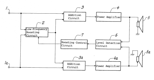
Fig. 2 shows the basic automati~c 1oudness control
circuit of the invention sho~n in Fig. l, as adapted for
use in a stereophonic audio signal reproduction system.
Th circuit of Fig. 2 comprises the circuit of Fig. 1
serving as a left signal,channel and a right signal
channel arranged in parallel,to,the left channel. The right
: ~ .
6-
':
,., ~ , . .
.
.
~36~1S~32
signal channel comprises an audio signal source la,
an addition circuit 3a, a power amplifier 4a and a loud-
speaker 5a, and shares the low frequency boosting circuit
2, the level detection circuit 6 and the boosting control
circuit 7 with the left signal channel.
The automatic loudness control circuit shown in
Fig. 2 for stereophonic audio signal reproduction will
be described in greater detail with reference to the
specific example shown in Fig. 3. In the circuit of Fig.
3, the left signal channel and the right signal channel
operate the same, so that a description will be given of
the left signal channel only, and the right signal channel
will not be described. Each circuit component of the
right signal channel will be designated by the same reference
number as the corresponding component of the left channel,
with the adscript a attached to the reference number.
The audio signal from the audio signal source 1
is fed to a first buffer amplifier 11 via a preamplifier 9
and a capacitor 10, these components thus providing a
signal channel for passlng the audio signal therethrough
without altering the frequency characteristics thereof.
~- ~ A capacitor 13 and a resistor 14 are connected
in parallel with the output termlnal of the capacitor 10
and have their output terminals connected together and
further connected to a first input terminal of an addition
: :
~ -7-
~'' '
.
~3~S~L32
amplifier 12, whereby the high-frequency component of
the audio signal through the capacitor 13 and the audio
signal of entire frequency range as attenuated by the
resistor 14 are mixed together to give a signal, which is
applied to the first input terminal of the addition
amplifier. The circuit from the output terminal of the
capacitor 10 to the first input terminal of the addition
amplifier 12 serves as a high frequency boosting circuit
for boosting the high-frequency component of the audio
signal.
Also connected to the output terminal of the
capacitor 10 is a first low-pass filter 15 comprising a
resistor 16 and a capacitor 17. The low-frequency
component of the audio signal passing through the low-pass
filter 15 is sent to a level control circuit 19 by way of
a second buffer amplifier 18. The output signal of the
boosting amplifier 20 to be described later and a contol
signal from the detection circuit 30 to be described later are
fed to the level control circuit 19, whereby the extent
of attenuation of the output signal from the second buffer
amplifier 18 is controlled. The attenuated output signal
;~of the second buffer amplifier is fed to the boosting
amplifier 20 and lS thereby boosted to a specified
magnitude.
The output signal of the boosting amplifier 20
-8-
,. :
~3~
is passed through a second low-pass filter 21 comprising
a resistor 22 and a capacitor 23 and then through a third
buffer amplifier 24, and is applied to a second input
terminal of the addition amplifier 12.
The circuit from the first low-pass filter 15
to the addition amplifier 12 serves as a low frequency
boosting circuit, whereby the low-frequency component
extracted from the audio signal is boosted to give a low-
frequency boost signal.
The output terminal of the addition amplifier 12
is connected to a power amplifier 25 via a capacitor 26
and a volume-adjusting variable resistor 27. The output
signal of the power amplifier 25 is applied to a loud-
speaker 29 and is also sent to the level detection circuit
30 via a detection resistor 31.
The level detection circuit 30 prepares a
level deteetion signal representing the output signal level
of the power amplifier 25 and feeds the signal to the
level control circuit 19 as a control signal.
A capacitor 28 and a manual switch 33 are
eonnected to another terminal of the level detection
eircuit 30. The manual switeh 33 produees an ON or OFF
: slgnal, which i5 sent to the deteetion eireuit 30 and to
a switching circuit 32.
Depending on whether the manual switeh 33 is on
'~ ~
_g_
~L3~
or off, the switching circuit 32 is set to a loudness
control mode or otherwise (loudness non-control mode) and
on-off controls the first and third buffer amplifiers 11,
24 and the addition amplifier 12 according to the selected
mode.
When the control circuit described above is not
set for automatic loudness control, the manual switch 33
is turned on to set the switching circuit 32 to the
loudness non-control mode. Consequently, the switching
circuit 32 produces a control signal, which brings the
addition amplifier 12 and the third buffer amplifier 24
out of operation, with the result that the output signal
from the preamplifier 9 passes through the first buffer
amplifier 11, is amplified by the power amplifier 25 and
is applied to the speaker 29. Thus, the audio signal from
the signal source 1 is amplified uniformly over the
entire frequency range without being boosted over the
low-frequency or high-frequency range and is released
from the speakex 29 as a sound.
For automatic loudness control, the manual switch
:
33 is turned off to set the switching circuit 32 to the
loudness control mode, whereupon the circuit 32 produces
-.
a control signal to deenergize the first buffer amplifier
.
11 and energize the addition amplifier 12, the third buffer
amplifier 24 and the leveI detection circuit 30.
1 0 -
.~,.,. ,,., ~
: .
Consequently, the output signal of the preamplifier 9 ls
attenuated by the resistors 14, 34 and sent to the addition
amplifier 12, while the high-frequency component of the
output signal is fed to the addition amplifier 12 via the
capacitor 13.
Since the audio signal channel from the signal
source 1 to the power amplifier 25 has no change-over
switch, the mode can be changed by the switching circuit
32 without producing any noise due to switching.
The output signals of the preampllfiers 9, 9a
of the two signal channels are mixed together by the
first low-pass filter 15 and then fed to the level control
circuit 19 via the second buffer amplifier 18. At this
time, the level detection signal from the level detection
circuit 30 and the output signal from the boosting
amplifier 20 are fed to the level control circuit 19 as
control signals, in accordance with which the output
signal of the second buffer amplifier 18 is level-controlled
before being applied to the boosting amplifier 20.
Consequently, the low-frequency component~is boosted by
the level control circuit 19 and the boosting amplifier
20 to a magnitude in conformity with the output signal level
of the power a~plifiers 25, 25a, such that the magnitude of
boosting decreases as the output signal level rises, or
increases as the output signal level lowers.
-11-
,
~3~5~L32
The output signal of the boosting amplifier 20
is applied to the second input terminal of the addition
amplifier 12 through the second low-pass filter 21 and the
third buffer amplifier 24 and added to the high-frequency
boost signal applied to the first input terminal of the
amplifier 12 before amplification. At this time, the
high-frequency component contained in the output signal
of the preamplifier 9 is amplified by the addition
amplifier 12 and then delivered, whereas the medium-
frequency component is attenuated by the resistors 14,34, thereafter amplified by the addition amplifier 12 and
therefore delivered from the amplifier 12 as a signal
component of substantially the same level as the output
signal of the preamplifier 9.
Consequently available at the output terminal
of the addition amplifier 12 is a mixed.signal composed
of the medium-frequency component of substantially the
same leveI as the output signal of the preamplifier 9
and the boosted h~gh- and low-frequency components. The
:20 mixed signal is amplified by the power amplifier 25,
applied to the loudspeaker 2g and released therefrom as
a sound. When the manufal switch 33 is off, accordingly,
the audio signaIs.are sub}ected ~o automatic loudness
: : control in accordance with the output signal level of the
: 25 power amplifiers 25, 25a.
12-
~3~S~L3~:
While the left channel addition amplifier 12
is in operation, the right channel addi-tion amplifier 12a
is also in operation, and the boosted low-frequency
component ohtained at the output terminal of the third
buffer amplifier 24 is applied also to the right channel
power amplifier 25a via the addition amplifier 12a, with
the result that the right and left channels are equal in
low-frequency signal level to assure acoustically natural
signal reproduction.
r~hen the output level of the audio signal source
varies as indicated in broken lines in Fig. 5, the audio
signal applied to the speaker has the frequency character-
istics shown in solid lines. More specifically, the low-
frequency component is boosted to an automatically
adjusted magnitude according to the output signal level
of the power amplifier as represented by solid lines 8a,
8b and 8c. Thus, the automatic loudness control circuit
of the invention affords optimum loudness characteristies
at all times. The high frequeney boosting eircuit
ineluded in the eontrol eireuit also boosts the high-
frequeney eomponent by a specified magnitude as indieated
in dot-and-dash lines in Fig. 5.
Most eomponents of the eireuit of Fig. 1 other
than the eapaeitors 10, 26 and 17, ete. ean be fabrieated
into an IC easily. IC fabrieation can therefore be realized
~ -13-
,
" 13~S432
more advantageously than conventionally possible.
Further since the low frequency boosting circuit
includes the low-pass filters 15, 21 preceding and
subsequent to the boosting amplifier 20, it is possible to
preclude clipping due to the high- and medium-frequency
components of the audio signal and to give an improved
S/N ratio unlike the case wherein the boosting circuit
comprises only one of the filters.
Not only the level detection signal from the
level detection circuit 30 but also the output signal of
the boosting amplifier 20 is applied to the level control
circuit 19, so that even if the level of the input audio
signal rises at a reduced volume given by manipulating
the variable resistor 27, the level control circuit 19
functions normally with the output signal of the boosting
amplifier 20~ This eliminates the likelihood that the
boosting amplifier 20 will reach saturation to result in
an impaired distortion factor.
The output control signal of the switching
circuit 32 is no* given to the second buffer amplifier
18, the level control circuit 19, the boosting amplifier
20 or the like, with the result that these circuits 18, 19
and 20 can be held in operation regardless of whether
the manual switch 33 is on or off. The manual switch 33
~: 25 is therefore operable without causing any potential
:~: -14-
~ :
:, j . , .
~3~1S~32
variation.
The manual switch 33 which can not be incorporated
into an IC need only be provided singly and can be
connected to the terminal of the level detection circuit
30 along with the capacitor 28, so that the present
circuit prepared in the form of an IC need not be provided
with a connection pin specifically for the manual switch.
Fig. 4 shows the level control circuit 19 and
the level detection circuit 30 of Fig. 3 in greater detail.
The input terminal 35 of Fig. 4 corresponds to the output
terminal of the second buffer amplifier 18 of Fig. 3.
The low-frequency component of the audio signal
applied to the input terminal 35 is sent to the boosting
amplifier 20 via the level control circuit 19.
In the level control circuit 19, the detection
signal from the level detection circuit 30 is applied to
the base of a first transistor 37. Connected to the
collector of the first transistor is a first current mirror
circuit 38 comprising second to fourth transistors 39, 40
and 41. The fourth transistor 41 has connected to its
collector a second current mirror circuit 42 comprising
fifth to eighth transistors 43, 44, 45 and 46. Connected
- to the collector of the sixth transistor 44 is a third
~current mirror circuit 47 comprising ninth to eleventh
25 transistors 48, 49 and 5Q.
-15-
'
~5~
A current in accordance with the detection
signal of the level detection circuit 30 flows through
the collector of the first transistor 37. The first
current mirror circuit 38 functions to pass a control
current of the same value as the collector current of the
first transistor 37 through the collector of the fifth
transistor 43. Since the collector current of the sixth
transistor 44 is equal to the collector current of the
ninth transistor 48, the second and third current mirror
circuits42, 47 function to make the collector currents
of the seventh, eighth, tenth and eleventh transistors
45, 46, 49, 50 equal to the control current through the
collector of the fifth translstor 43. Accordingly, the
collector currents of the seventh, eighth, tenth and
15 eleventh transistors 45, 46, 49, 50 can be varied at the
same time in accordance with the magnitude of the detec
tion slgnal of the detection circuit 30 while being
maintained at equal values.
Connected between the second current mirror
circuit 42 and the third current mirror circuit 47 is
a variable impedance circuit 51 comprising bridge-connected
first to fourth diodes 52, 53, 54, 55. Each of these
: diodes 52 to 55 comprises a Schottky barrier diode. The
anodes of the first and second diodes 52, 53 are connected
: 25 together, and the collector of the eleventh transistor 50
-16~
3;;~
is connected to the connection. The anodes of the third
and fourth diodes 54, 55 are connected together, and the
collector of the tenth transistor 49 is connected to the
connection. The cathodes of the first and fourth diodes
52, 55 are connected together, and the connection is
connected to the collector of the eighth transistor 46.
The cathodes of the second and third diodes 53, 54 are
connected together, and the connection is connected to
the collector of the seventh transistor 45. The
connection of the third and fourth dlodes 54,55 are
connected to a signal reference voltage.
Consequently, the eleventh transistor 50 serves
as a first current source for supplying a bias current to
the anodes of the first and second diodes 52, 53, and
the tenth transistor 49 serves as a second current source
for supplying a bias current to the anodes of the third
and fourth diodes 54, 55. The eight transistor 46 serves
as a third current source for withdrawing a current from
the cathodes of the first and fourth diodes 52, 55. The
seventh transistor 45 serves as a fourth current source
for withdrawing a current from the cathodes of the second
and third diodes 53, 54. Further the fifth transistor 43,
the sixth transistor 44 and the ninth transistor 48
constitute a current control circuit for varying the
currents through the first to fourth current sources while
maintaining the currents at substantially equal values.
The connection between the anodes of the first
:
-17-
~3~43Z
and second diodes 52, 53 serves as a signal terminal for
the variable impedance circuit 51, and a resistor 36
is connected between the signal terminal and the input
terminal 35 to cause the resistor 36 and the impedance
circuit 51 to voltage divide the signal fed to the input
terminal 35 to control the extent of attenuation of the
signal to be fed to the boosting amplifier 20.
With the level control circuit 19 described
above, the impedance of the variable impedance circuit 51
as viewed from the signal input terminal is controlled
based on the detection signal from the level detection
circuit 30, whereby the level of the signal to be fed
to the boosting amplifier 20 is controllable.
The output terminals of the left power amplifier
25 and the right power amplifier 25a are connected to
each other via a first detectlon resistor 31 and second
detection resistor 31a. The connection is connected to
the level control circuit 19 via the level detection
circuit 30 which comprises a comparative amplification
circuit 56 and a twelfth transistor 57. The amplification
circuit 56 has a positive input terminal connected to the
.
connection between the resistors 31, 31a and a negative
input terminal which is grounded. The amplification
circuit 56 feeds an output signal to the base of the
twelfth transistor 57, whereby the transistor is brought
~ :
-18-
:
~L3~
into or out of conduction. The capacitor ~8 for smoothing
the output signal of the transistor is connected to the
collector of the twelfth transistor 57. Accordingly, a
current in accordance with the terminal voltage of the
capacitor 28 flows through the first transistor 37
constituting the level control circuit 19.
The collector of the third transistor ~0
included in the first current mirror circuit 38 is connected
to the positive input terminal of the comparative amplifi-
cation circuit 56, thus forming a feedbac~ channel to theamplification circuit 56.
When the output signals of the left and right
power amplifiers 25, 25a are positive relative to a
reference level, the comparative amplification circuit 56
produces "H" output since the negative input terminal of
the circuit 56 is grounded, turning off the twelfth
transistor 57. Accordingly, the capacitor 28 is not
charged, and the second~transistor 39 of the first current
mirror circuit 38 is held off, with no bias current
supplied to the variable impedance circuit 51. Consequent-
ly, the signal applied to the input terminal 35 is fed
- to the boosting amplifier 20 and amplified thereby without
being attenuated by the impedance circuit 51.
When the output signals of the left and right
~25 power amplifiers 25, 25a become negative relative to the
~: : . -19
~36~;4L32
reference level, a current flows through the first
detection resistor 31 in the direction of arrow shown,
thereby causing the comparative amplification circuit 56
to produce "L" output to charge the capacitor 28. While
the negative output signal level of the left amplifier
25 is low at this time, the terminal voltage of the
capacitor 28 does not build up, and the first transis-tor
37 remaining off to hold the impedance circuit 51 unener-
gized. When the negative output signal level of the
left power amplifier 25 rises, the output of the amplifi-
cation circuit 56 lowers sufficiently to increase the
collector current of the twelfth transistor 57, thereby
raising the terminal voltage of the capacitor 28 to turn
on the first ransistor 37.
When the first transistor 37 is brought into
conduction, the first to third current mirror circuits
38, 42, 47 function, passing through the impedance circuit
~ 51 a current in conformity with the detection signal of
: the level detection circuit 30. Suppose the input-ouput
: 20 current ratio of the first current mirror circuit 38 is n1,
:and the input-output current ratio of the second and
third current mirror circuits 42, 47 is n2. The current
flowlng through the first to fourth diodes 52 to 55 of the
: variable impedance circuit 51 has the value of :n1n2I1
: ~ ~
~wherein I1 is the collector current of the first transistor
.
: ~ -20-
:
:
,:. ~: .: ~:
;432
37. The impedance values of these diodes are in conformity
with the current value n1n2I1. Consequently, the signal
applied to the input terminal 35 is voltage-divided by
the resistor 36 and the combined impedance of the first
to fourth diodes 52 to 55 for attenuation and thereafter
amplified by the boosting amplifier 20.
Further when the first transistor 37 conducts,
a current:n1I1 proportional to the collector current of
the transistor flows through the collector of the third
transistor 40 of the first current mirror circuit 38, then
through the feedback channel into the first detection
resistor 31, consequently deenergizing the comparative
amplification circuit 56 and turning off the twelfth
transisor 57. Nevertheless, the first transistor 37
remains on since the capacitor 28 has a sufficiently great
discharge time constant, holding the impedance circuit
51 also in operation. The amplification circuit 56 is
thereafter brought into operation when the level of the
negative output signals of the power amplifiers 25, 25a
rises to such an extent as to pass a current greater than
: the collector current :n1I1 through the third transistor
; 40. Thus, the level detection circuit comprising the
amplification circuit 56, twelfth transistor 57, capacitor
28 and the feedback channel from the third transistor 40
functions as a peak current detection circuit which gives an
: .
~'
32
output waveform holding the peak of the input current
waveform.
The circuit operation described above will be
summarized as follows. When the output signal level of
the left and right power amplifiers 25, 25a eYceeds a
predetermined value, the variable impedance circuit 51
functions to attenuate the input signal to the input
terminal 35 according to the Outp-lt signal level, and
the input signal is held attenuated in conformity with
the discharge time constant of the capacitor 23. only
when an output signal is given which is higher than the
output signal level, the comparative amplification circuit
56 thereafter functions to control the variable impedance
circuit 51 so that the impedance of this circuit becomes lower.
~ccordingly, the automatic loudness control
circuit of Fig. 3, when incorporating the above circuit,
effects loudness control in accordance with the level of
the sound signal to be released from the speakers,
consequently giving the frequency characteristics
20~ represented by the solid lines 8a, 8b, 8c in Flg. 5.
Furthermore, even when the varlable resistor 27 is
manipulated to alter the volume from large to small, the
smoothing function of the capacitor 28 precludes marked
low frequency boosting. The reproduction therefore will
~ not sound strange.
-22-
: ~ :
~ : .
' ~ .
,
: "
32
The variable impedance circuit 51 included in
the level control circuit 19 of Fig. 4 comprises Schottky
barrier diodes and is accordingly about 0.4 V in the lowest
operating voltage, such that a sufficient dynamic range
is available even if the power supply used has a voltage
as low as 1.5 V. Since the Schottky barrier diode
affords an impedance e~uivalent to that of a PN junction
diode with a relatively low bias voltage, the circuit
can therefore be easily fabricated in the form of
an IC.
With the circuit shown in Fig. 4, the output
signal level of the left and right power amplifiers 25,
25a is detected in the current mode, so that even if the
detection resistors 31, 31a are made to have such a small
resistance value as to be fabricated into the IC, no
crosstalk occurs between the output signals of the two
power amplifiers 25, 25a. The impedance of the variable
impedance circuit 51 is controlled with a current in
accordance with the output signal level of the power
ampli~iers and is therefore less susceptible to the
influence of variations in the transistor characteristics.
Accordingly, the impedance lS controllable with high
accuracy, permitting the level control circuit l9 to
operate normaIly even in the presence of some variations
~in the power suppIy voltage.
23-
,,, .,, ~ . :
. -
' ~
' ' ' '
. , .
5~32
The construction of the present circuit is not
limited to those of the foregoing embodiments but can be
modified variously by one skilled in the art without
departing from the scope of the invention as defined in
5 - the appended claims.
-24-
' ~ .