Note: Descriptions are shown in the official language in which they were submitted.
L30~i5Cl~
The invention relates to a display device comprising a
substantially evacuated envelope having mainly flat, substantially
parallel front and rear walls, a layer of luminescent material along the
inner surface of the front wall and ~eans for generating at least one
electron beam which moves substantially in a plane parallel to the
front and rear walls and which can be selectively deflected in the
direction of the layer of luminescent material v a deflection
~eans in a deflection unit, so that each beam scans at least a pa~t of
the layer of luminescent material, said device for generating electrons
comprising at least one cathode unit having at least one cathode which
can be controlled separately.
The invention also relates to a cathode unit for use in a
display device of the type described.
A display device of this type has great advantages
because it provides the possibility of realizing thin flat television
screens. Research is being done into constructions of such types that
the;thick glass walls, which are often~necessary in connection with the
high vacuum, can be avoided as ~uch as possible. Other points of
research aim at obtaining a uniform brightness throughout the picture
surface, independent of the driven pixel and the possibility of
integrati~n with control electronics.
A display device of the type described in the opening
paragraph is ~nown from Netherlands Patent Application No. 7610521 laid
op~en ~o public inspection.
25~ ~ In this device electron beams are guided through channels
and subsequently they are not only deflected to the phosphor screen, but
the beams also perfor~a scanning movement in the transverse direction
of the channel. ~he latter is effected to simplify the electron gun for
such a device.~ In this case~either a source for one beam or a line
cathode arranged on or along the end wall of the channels, xespectively,
is used.
The dimensions of conventional cathodes are such that
,~
" . .. : . ,
3~5~9
PHN 12.337 2 17.03.1988
generated electron beams of two cathodes located at a mini~um distance
from each other enclose a plurality of pixel columns, t~us requiring a
horizontal deflection over a plurality of pixels. ~oreover, the energy
supplied is so high that the solution proposed in the above-cited Patent
Application is extremely costly on qrounds of energy considerations and
extra material costs (hori.zontal deflection electrodes in the
channels).
The use of semiconductor cathodes in different display
devices has already been proposed, notably in the Netherlands Patent
Application No. 7905470 (PHN 9532) in the name of the Applicant.
However, such cathodes have the drawback ~hat, although they amply meet
the requirements imposed on dimensions for use in a device in accordance
with NL 76105~1, their efficiency rapidly deteriorates due to an ion
bombardment caused by positive ions which are created notably in the
high-voltage section of the device.
To prevent this, a preferred embodiment of a display
device according to the invention is characterized in that the cathode
unit comprises deflection means and in that a row of electron
multipliers is arranged in the beam path between the cathode and the
deflection unit.
The cathode is preferably a semiconductor cathode in
; which the main surface of the semiconductor body is preferably
; substantially perpendicular to the plane in which the electron beams ~ove.
In this case it is not absolutely necessary fo~ the
emissive surface to coincide with the main surface of the se~iconductor
body. For example, the cathode may be in the form of one or more
punctiform emitters as described in the Netherlands Patent Application
~L 7905470 laid open to public inspection.
The invention is based on the recognition that the
assembly of cathode, deflection means and electron multipliers
functions, as it were, as an ion trap due to the deflection of the
electron beam between the ca~hode and the electron multipliers.
This ensures a longer lifetime of the cathode. This
i~provement is all the ~ore effective as the total number of required
(semiconductor) cathodes in the entire display device can be reduced,
for exa~ple, by increasing the number of columns driven by one cathode.
..
55~D9
PHN 12.337 3 17.03.1988
Since horizontal deflection takes place prematurely, the
channels as described in the Netherlands Patent Application 7610521 laid
open to public inspection can be dispensed with.
However, deviations due to the earth s magnetic field
which are largely corrected in conventional tubes by means of electron-
optical systems must now be avoided in a different way.
To this end the plane within which the electron beams
move parallel to the front and rear walls is substantially entirely
surrounded by a Magnetic shield whose outer cladding may also function
as a high-voltage electrode.
There are various possibilities for the display after the
deflection of the electron beam from the plane parallel to the front
and rear walls.
For example, the so-called penetration principle may be
chosen ~for example, in the case of two colours), by which the voltage
at the front wall is varied dependent on the colour to be displayed. The
so-called index principle may be used alternatively.
However, the display device preferably comprises a shadow
mask (which ~ay be provided, if necessary, wi~h de~lection electrodes).
The shadow mask may form part of the above-mentioned magnetic shield
unit. For the display of a picture two (~onochrome) or six ~colour) line
;memories are required in this case for displaying the previous picture
or storing the next (sub-)picture.
A light valve~may also be arranged in front of the front
wall, for example, a liquid crystal device successively passing the red,
green and blue sub-pictures. In this case the device should be provided
with picture memories.
A cathode unit according to the invention comprises at
least one cathode, deflection means for one or more electron bea~s and a
row of electron multipliers.
The invention will now be described in greater detail, by
way of example, with reference to the accomPanying drawing in which
Fig. 1 is a diagrammatic cross-section of a display
device according to the invention,
35Fig. 2 is a cross-section along a part of the device of
Fig. 1, perpendicular to~the cross-section shown in Fig. 1,
Fig. 3 ia a cross-section of a separate cathode unit.
,. .
.
~3~S~9
PHN 12.337 4 17.03.1988
The drawings are diagra~matic and not to scale;
corresponding components usually have the sa~e reference numerals.
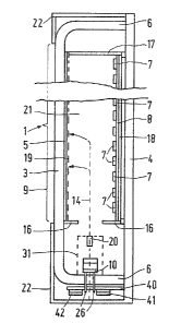
Fig. 1 is a diagral~matic cross-section of a display
device 1 according to the invention, comprising a substantially
evacuated envelope having a front wall 3 and a xear wall 4. Together
with the side walls 6, the front wall 3 forms part of a glass lid or tub
having an overall height of, for exa~ple, 5 cm, whilst the rear wall 4
in this embodiment is in the form of a thin steel wall which may have
reinforcement ribs, if necessary. A layer of lum:Lnescent material, for
example, a phosphor screen 5 is present on the inside of the front wa]l
3.
The display device 1 also comprises means for generating
a plurality of electron beams 14 which move at least substantially in
a plane parallel to the front wall 3 and the rear wall 4 before they
are deflected in the direction of the phosphor screen 5. The electron
beams move not only parallel to the front wall 3 and the reax wall 4 but
also substantially perpendicular to the picture lines of the picture to
be displayed, because horizontal deflection is effected in the cathode
unit 31 before the electron beams reach the deflection unit which is
20 bounded by the walls 3, 4 and the end walls 16, 17. The pho~phor parts
to be impinged on (in other words, the picture line to be activated) are
selected via voltages at deflection electrodes 7 arranged on an
insulated carrier 8 in this e~bodiment. The electron beams 14 are
thereby deflected to the phosphor screen 5.
The electrons are generated by means of semiconductor
cathodes 10, which may be controlled separately, and they are
subsequently accelerated by electrodes 24, thereby forming electron
beams 14, whilst the emissive surface 12 extends perpendicularly to the
walls 3, 4 in this e~bodiment. The electron beams 14 are deflected by
means of deflection electrodes 15 directly after the formation of the
beam.
According to the invention a ro~ of electron multipliers
20 is arranged between the deflection electrodes 15 and the high-voltaye
section 21 in which the deflection towards the phosphor screen 5 takes
place. Subsequently the electron bea~ 14 (intensified by the operation
of the elect.ron multiplier) moves substantially parallel to the front
wall 3 and the rear wall 4 and also perpendicularly to the end walls 16,
.
'; . :
', ' : ,
~3~ 9
PHN 12.337 5 17.03.1988
17.
The electron multipliers 20 have a dual function. On the
one hand electron multiplication is effected so that a picture of
greater intensity can be obtained. On the other hand possible positive
ions, which are generated by the electrons in the high-voltage section
21 and accelerated by the dominant field in the direction of the cathode
unit, are captured by the electron multipliers 20 so that they cannok
damage the cathode 10.
In the device as shown in Figs. 1 and 2 the deviation
which the beams 14 may acquire with the aid of the deflection electrodes
15 is chosen to be such that each cathode covers, for example, n
columns. The cathode unit 31 is thus seemingly split up into a plurality
of sub-units denoted by means of broken lines 23. The deflection
electrodes 15 and the cathodes 10 are now controlled by means of
periodical deflection voltages at the deflection electrodes 15 and
information from a line register 41 in such a manner that the
information associated with the relevant line is presented to the
columns 1, n+1, 2n+1 .... at instant t1 ; to the columns i, n+i, 2n+i
at instant ti (1<i<n), and to the columns n, 2n, 3n, ...., 3n .......
at instant tn. After the information of the next line to be written is
written in the line register 41 and the control of the line electrodes 7
(for example, via a switching element not shown) has ~een adapted,
this procedure is repeated. For electrical connections of the cathodes
and other elements the walls 6 have lead-throughs 26 with which possible
acceleration eIectrodes 24 can be controlled and with which the voltage
for the electron multiplier is ensured, for example, via contact
conductors 25.
The electron beams 14 from the cathodes 10, deflected by
the electrodes 15 and intensified in the electron multipliers 20, are
subsequently accelerated parallel to the front and rear walls before
they reach the actual display section 9. These electrons may exhibit
deviations from their straight path under the influence of the earth s
magnetic field, whilst a lateral correction is not possible. For this
reason the plane within which the electrons are accelerated and move
parallel to the front and rear walls is substantially entirely
surrounded by a magnetic shield, formed in this embodiment from a cage-
like construction comprising, for example, the carrier 8 for the
s~
PHN 12.337 6 17.03.1988
electrodes 7 whose lower side is to this end provided with a metal
layer or metal pattern 18l whilst the device comprises an electrically
conducting bush connected thereto having ~ first wall 16 ~also high-
voltage grid) and an end wall 17, the assembly being maqnetically closed
by the shadow mask 19. Other, more open constructions are alternatively
possible in which, as in this embodiment, genera]Lly known methods of
demagnetizing can be used, if necessary. The electrodes 7 can be
controlled via control circuits ~not shown) which are also arranged,
for example, on the carrier 8 and are contacted by mean5 of metal tracks
(not shown) projecting outside the side wall 6.
The vacuum space can be built in a protective cabinet 22
leaving free the visible part of the picture and accommodating operating
elements as well as control circuit elements 41, 42 arranged on, for
example, a printed circuit board 40.
As already described in the opening paragraph, there are
various possibilities for the display of the picture after the electron
beam 14 has been deflected towards the phosphor screen 5. For example,
in the case of colour display the penetration pxinciple may be used,
notably when using display tubes with at most two colours, ox the so- -
called index principle may be used.
In the device shown the phosphor screen 5 is split up,
for example, into horizontal tracks of luminescent material. The
infor~ation for each of the three colours is presented during 1/3 of the
line period, whereafter the voltaqes at the deflection electrodes are
slightly changed and the information for the adjacent colour track is
presented during 1/3 of the line period, etc. Since the (colour)
information is simultaneously read in the case of TV display and is then
presented serially in accordance with the incoming signal, the colour
information is temporarily stored in line me~ories. Each colour to be
displayed requires two line memories, namely one for the line which is
being read and a second in which the next line is stored.
Another possibility is the use of so-called light valves
in which a monochrome tube is controlled each time during 1/3 of the
picture period with the red, the green and the blue picture signal,
respectively, whilst light valves, for example, LCDs with red, green or
blue colour filters arranged in front of the tube are synchronously
switched on. In this case the presence of picture memories is required.
,
.
.
~.3~S~9
PHN 12.337 7 17.03.1988
In the device of Fig. 2 the cathodes 10 are secured to a
side wall 6 of the envelope 2 of the vacuum space. The cathode unit 31,
with cathodes 10, acceleration electrodes 24, deflection electrodes 15
and electron multipliers 20 may of course also be manufactured
separately in a glass envelope 11 which is secured to the end of the
vacuum space at a later stage of manufacture.
The sub-units denoted by the broken lines 23 may also be
manufactured separately as shown in Pig. 3, and may subsequently be
secured next to one another. This has the advantage that the separate
units can be individually tested and replaced, if necessary. The number
of electron multipliers in the device of Fig. 3 may of course also be
extended in such a way that all columns of the picture can be covered by
means of one cathode 10. If necessary, a thermal cathode instead of a
semiconductor cathode may of course be used alternatively.
, . .
.