Note: Descriptions are shown in the official language in which they were submitted.
~3~
FA070.2
OPTICAL DISK DRIVE DEVICE
AND INFORMATION STORAGE DEVICE
FIELD OF THE INVENTION
The present invention relates to an optical disk drive
device, and more particularly, to an optical dlsk drive
device which controls access of a light spot to an arbitrary
track on an optical disk.
The present invention also relates to optical disk
devices or similar information storage devices which have a
head movable with respect to an optical disk, etc.D and can
write, read or erase the information.
: ` :
The present invention also relates to an information
storage device capable of recording. reproducing, or erasIng
the informatlon on or from an information storage medium
having multiple tracks. More specifically, the invention
relates to an information storage device, which even in the
case of failure of a seeking operation or the like can be
quickly controlled for stable operation.
: 1
:
``: :
. ~ .
,'
' t'
, . . . .
'
,
13~5 7~ FA070.2
BRIEF DESCRIPTION OF T~IE DRAWINGS
Fig. 1 a block diagram of a known optlcal dlsk drlve
device.
F'ig. 2 is a block diagram of the velocity-control
system used in the known optical disk drive device.
Flg. 3 shows high-frequency-band resonance frequency
characteristics of the mechanical system.
Fig. 4 shows an example of frequency characteristics of
a notch filter built ln the velocity-colltrol system of Fig.
; 2.
Flg. 5 and Fig. 6 respectively show examples of the
open-loop characteristics of the velocity-control system
shown in Fig. 2.
Fig. 7 is a dlagram of another known device.
Fig. 8 shows waveform explainlng operation of the known
device of Fig. 7.
Fig. 9 is a block diagram of the optical disk drive
device of an embodiment of the lnvention.
Fi~. 10 is a blcck diagram of the velocity-control
system incorporated in the optical dlsk drive device.
Flg. 11 is a diagram which explains the operatlon of
the state-observer unit in the optical disk drive device.
Fig. 12 is a diagram which explains the operation of
the direction-detectlon circuit o~ the optical disk drive
device.
I
~ ~t7~ FA070.2
Fig. 13 1s an example of an open-loop transfcr
characteristic of the velocity-control system of Fig. 10.
Fig. 14 is a block diagram of a velocity-cos~trol system
of the optical disk drive system of another embodiment of
the invention.
Fig. 15 is a diagram showlng a modificatlon O-e the
optical disk drive system of Fig. 9.
Fig. 16 is a block diagra~ of the optical disk drive
dev~ce of another embodiment of the invention.
Fig. 17 is a block diagram of the velocity-control
system incorporated in the optical disk drive device.
Fig. 18 is a block diagra~ of another velocity-control
system which can be built in the same optical disk drive
device.
Fig. l9 a block diagram of another velocity-control
system built ln the optical control system.
Fig. 20 ls a dlagram which explains the operation of
the track-traversing detection circuit in the optical disk
drive device.
Fig. 21 is a diagram ~hich explains the operation of
the direction-detection clrcuit of the optical disk drive
device.
Fig. 22 is an exsmple of an open-loop transfer
characteristics of the velocity-control system of Fig. 17.
Fig. 23 is a block dia~ram of the device of another
~ . .
~3~S 7~ FA070.2
embodiment of the lnventlon.
Fig. 24 and Fig. 25 show electric circuit diagrams of
the elements of the device.
Fig. 26 to Fig. 28 are time charts which illustrate the
operatlon of the device.
Fig. 29 -to Fig. 31 are explanatory diagrams whlch show
the area of linear output signals.
Fig. 32 is a block diagram illustrating a device of in
another embodiment of the invention.
Fig. 33 is block diagram of a velocity control system
for the device.
Fig. 34 is a diagram which illustrates some details of
the elements of the system.
Fig. 35 is a diagram showing details o~ the track
traverse velocity detectlon means used in the device of the
above embodiment.
Fig. 36 to Fig. 38 show waveforms of slgnals used for
explanation of operation of the device.
Fig. 39 is a block diagram o-f a modification of the
device of the above embodiment.
./~i~ i
~ ~'
~3~7~2 ~070.2
BACKGROUND OF TIIE INVENTION
Fig. 1 shows a block diagram of an access control
system described in Japanese Patent Applicatlon No.
101,439/1985 filed by the assignee of the present
application on May 15, 1985 and entitled "Optical
Disk Drive Device".
As illustrated, an optical disk 101 has a plurality of
recording tracks on the disk. The tracks comprise series of
pits disposed at a hlgh density and arran~ed in a circular
or spiral form. The disk 101 is fltted onto a spindle and
is rotated by a disk-drive motor 102. The disk-drive motor
102 is rotated under the control of a disk-mo$or-drive
control system 103.
An optical head 104 forms a light spot on the optical
disk 101. The light spot is moved in the radial direction
of the optical disk 101. The optical head 104 comprises a
frame 105, a source of light such as a semlconductor laser
106, a collimating lens I07, a polarization beam splitter
108~ a A /4 plate 109, an optical-path changing mirror 110,
an ob~ective lens 111 which focuses the light beam f`rom the
light source 106 onto the medlum surface of the optlcal disk
101 and forms a light spot 115 on the sur~ace, a tracking
actuator llZ which provides flne or microscopic mo~ements of'
the ob~ective lens 111 in the radial direction o~ the
* Published November 18, 1986
....
~3~ -t7~ FA070.2
optical disk 101 for accurate positionlng of the llght spot
on a recording track of the optical disk, and a split-
photodetector 113 which has a pair of sensor parts adJacent
to each other for detecting the return l:lght reflected from
the optical disk 101, and produces a pair of electrlcal
signals corresponding to the amount of light received at the
respective sensor parts.
An addition/subtraction amplifylng circuit 114
determines the sum of the outputs from the split-
photodetector 113 to produce a sum signal as an information
signal (reproduced data signal), and determines the
di-fference between the outputs of the split photode-tector
113 to produce a difference signal as a tracking error
signal. The tracking error signal is supplied to a track-
traverse counter 118 and a speed-detecting circuit 120.
The track-traversing counter 118 receives the output
signal from the addition/subtraction amplifying circult 114
and detects the number of tracks traversed by the optical
head 104. An output of thls counter 118 is supplied to a
target-velocity generation circuit 119.
The target-velocity generation circuit 119 recelves the
output signal of the track-traversing counter 118, and, at
the time of access, generates a target-velocity signal for
the llght spot 115. The target-velocity signal is sent to a
head-actuator drire control clrcuit 117.
~ 7~ FA070.2
The head-actuator driYe control circuit 117 also
receives an output signal from a polarity switchin~ circuit
2. On the basis of these signals, the head actuator drive
control circuit 117 controls the drive o~ a head actuator
116, such as a llnear actuator.
When the head actuator 116 is drlven through the head-
actuator drive control circuit 117 to move the optical head
104 in the radial directlon of the optical disk 101.
A speed detection circuit 120 detects the track-
traverse speed (the speed wlth which light spot 115
traverses the tracks on the optical disk 115). The output
of the speed detection circuit 120 is fed to the polar,lty
switching circuit 2. The speed detection circuit 120,
together with the polarity-switchin~ circuit 2, forms a
velocity-detection circuit 124.
The polarity-switching circuit 2 receives an output
signal from an access-direction command ~eneration circuit
123. Under the control of the output signal of the access-
direction command generation circuit 123, the polarity-
switching circuit 2 changes the polarity of the output of
the speed detection circuit 120. More speciflcally, the
detected speed ~a scalar value) is converted into a detected
velocity (a vector value~ which also shows the direction.
Fig. 2 is a transfer-function block dla~ram of the
velocity-control system which represents the diagram Or Fig.
. `
A
13~579Z FA070~2
1. In this drawing, the results of the subtraction between
the output signal Vs~ o-f the velocity detectlon circuit 124
and the output signal ~r f the target-velocity generation
circult 119 is input to a gain compensatlon circuit 5. The
gain compensation circuit 5 determines the frequency band of
~ the veloclty control system.
; The gain compensation circuit 5, as well as a notch
filter 122 and a head-actuator drive circuit 6, are built
into the head-actuator drive control circuit 117.
; The notch filter 122 compensates the mechanical resonance
~ characteristics GL(S) of a block 6 in -the head actuator 116.
; The head-actuator dr~ve circuit 6 is normally of a
current drive type, and also contains a drive current
detection circuit.
A block 7 in the head actuator 116 represents a force
constant of the head actuator 116. The block 8 represents
transfer characteristics. Its input is an acceleration, and
its output is a head velocity VL (the velocity with which
the optical head 105 ls moved by the head actuator 116). M
designates the mass of the movable part, GL(S) designates
the mechanical resonance characteristlcs of the head
actuator, and S represents Laplacean. KV represents the
sensitivity in the velocity detection of the target-velocity
generation circuit 119 and the velocity-detection circuit
124, and ~ represents the track traverse period (period
;
'.
i3~ 7~ F~070.2
taken for the light spot 115 to kraverse a track).
Fig. 3 shows an example of gain characteristic of GL(S)
in the block 8 in Fig. 2 which is shown to have a large
resonance peak at a certain frequenc~ ~ L (usually in the
order of kllz). Fig. 4 on the other hand illustrates the
galn characteristics IGN(S)I of the notch filter lZ2 in Fig.
2. Gn(S) is selected so that:
IGN(S~I _ Il/GL(S)I.
when
~ N = ~ L-
Fig. 5 and Fig. 6 show open-loop characteristics of the
system of Fig. 2. Fig. 5 shows a case where GN(S) =
1/GL(S), while Flg. 6 shows a case where GN(S) ~ l/GL(S).
The system operates in the following manner:
First, the disk drive motor 102 is energized through
the dlsk-drive-motor control circuit 103, and the optical
disk 101 shown in Fig. 1 begins to rotate. When the
rotation speed reaches a predetermined steady value, the
tracking actuator 112 ls controlled on the basis of a
tracking error signal obtained by the photodetector 113 and
addition~subtraction amplifying circuit 114. As a result,
the light spot llS begins to follo~ the center of a track on
the op-tical disk 101.
At the time o~ track access, the number of tracks on
the optical disk 101, which have been traversed by the light
~f~ ',
~i'
1 3~ 7~2 FA070.2
spot 115, ls counted by the track-traversing counter 118,
and, at the same t~me, in uccordance with the number o~
tracks to be traversed to reach the target track, the target
velocity, which is output from the tar~et-velocity
generation circuit 119, and the track-traverse velocity of
the light spot 115, which ls detected by the velocity-
detect~on circult lZ4, are input to the head-actuator drive
control circuit 117, which performs velocity control in
which the velocity is reduced to zero as the light spot 115
approaches the target track.
Operation of the velocity control sys-tem o-f' Flg. 2 at
; the t.ime o~ track access will now be described in detail. A
velocit~ deviation signal Ve, which is the difference
between the target-velocity slgnal Vr from the target-
velocity generation circuit 119 and the detected-velocity
signal Vs* from the velocity detector 124, is transmitted to
the actuator drlve clrcuit 6 through the ~ain-compensation
circuit 5 and the notch filter 12Z. As a result, a certain
drive current ls applied to the head actuator 116. Due to
this drive current, the head actuator 116 begins to move the
optical head 104, causing the light spot llS to traverse the
tracks on the optical disk 101.
If the track fluctuation velocity, due for example to
eccentricity of the optical disk 101, is denoted by Vd, the
dif~erence between the velocity of the head actuator 116 and
: 10
~ 7~2 FA070.2
the track fluctuatiorl velocity YO ls detected by the
veloeity detection clrcuit 1~4 as a detected-velocity signal
Vs*. This detected-velocitY signal Vs~ :Ls fed back in a
velocity control system and the control :Ls so made that the
detected-velocity signal Ys~ coincldes wLth the tar~et-
velocity signal Vr.
A loop transfer function (open-loop characterlstics) of
this velocity-control system from the velocity-deviation
signal Ve to the detected-veloclty signal vs* can be
expressed as follows:
) KcKAK~Kv GN(s)GL(s) Sr
(1)
.~ .
If it is so designed that the condition GN(S) = 1/G~S)
is satisfied, the head actuator does not have the resonance
frequency in the hi~h-frequencY zone, as shown in the upper
part of Fi~. 6. But if GN(S) ~ l/GL~S) because of
manufacturing fluctuations between individual devices, the
head actuator may have a resonance frequency in the high-
frequency band as shown in Fig. 6. When the peak of this
resonance exceeds db~ the velocity-control system loses its
stabllity.
Moreover, because of a certain dead time of the zero-
order hold characteristics of the velocity-detection circuit
lZ4, a long delay in phase is observed in the vicinity of
11
~3~?~ 7~Z
the track-traversin~ frequency.
Because of the con~lguration described above, the
conventional optical disk drive device had the followin~
problems:
(l) The track traverse velocit~ ls detected based on
the track traverse period. When the traverse is made at a
low veloclty, a time delay (dead time) is lengthened, and
the velocity control system loses its stability, and because
the cut-o-ff frequency o~ the velocity-control system must be
designed low, the velocity deviation will be increased.
(2) When the light spot 115 traverses drop-out or data
address recording portions. such traverse may erroneously be
recognized as traverse of tracks, and, in spite of -the slow
movement of the light spot, the velocity detection circuit
124 erroneously operates as if the track traverse velocity
were high. The result is that the velocity control system
is disturbed.
~ 3) The head actuator 116 typically has a high
mechanical resonance at the frequencY of several kllz. In
order to eliminate this phenomenon, a notch filter 122 is
built in the head actuator drive-control system. If,
however, there are a plurality o~ resonance frequencies, a
plurality of notch filters need to be provided, and the size
of the circuit of the system is thsrefore enlarged. In
addition, where there are dif-ferences in the resonance
12
' .
'-; ~!
~3~7~ ~A070.2
frequency from one device to another, and the resonance
-frequellcies differ from the frequencles of the notch
filters, and the velocity-control system is not stable.
- (4) Because the known system does not detect the
direction in which light spot 115 traverses the tracks, but
simply assumes that the light spot 115 is traversing the
tracks in the direction (toward the inner or outer perlphery
O-r the disk) in which the access is to be made and
determines the required veloclty by changing the polarity Oe
the speed. When the ~peed ls low, and the direction in
which the track is traversed is reversed due to track
fluctua-tion or disturbances, a positive feed-back is applied
to the system, and the optical disk may behave erratically.
Another problem of the above-described optical disk
drlve device is described below:
As the above-described optical disk drive device
obtains head position control informatlon from the optical
dlsk, the absolute position of the head cannot be reliably
detected when operation of the servo-system is disturbed, e.
g., in case of application o-~ a large external impact force.
In that case, as well as in the case of abnormal operation
of *he servo-system the head may run out of the proper range
toward the center or periphery of the disk and collide with
a stopper located at the end of the range of mobility. As a
result of this collision, the head recelves a blow and can
13
," ~ 4i
. .,_
~ 7~2 ~Ao70.2
be broken.
The same problem relates to magnetic disk devices. or
any other equivalent information storage devices.
Another example of prior art is explained below with
reference to Figs. 7 and 8.
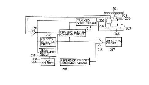
Fig. 7 illustrates a block diagram which shows a
control system of a known optical disk drlve device
published in Papers from the General Meet;ing of the
Instltute of Electronics and Communications Engineers (IECE)
of Japan, 1985, Vol. 7, pp. 7-76 [1170, "Track Access in a
Two-Stage Servo-sYStenl'', by }3iroshi Inada and Shigeru
Shimono]. Fi~. ~ illustrates waveforms of control slgnals
used in connection with the device shown in the block
diagram. In these drawings, reference numeral 201
designates an optical disk for recording information, or
with information already recorded on trac~s which are
arranged in the form of equally-spaced concentric circles or
ln the form of a spiral. Reference numeral 202 designates a
light beam by means of which informatlon is transferred to
and from the optical disk. A head actuator, e.g., a linear
actuator 205 drives a carrla~e 204 of an optical head 203
and moves the carriage 204 wlth respect to the optical disk
201 and across.the tracks. A tracklng actuator 206 i5
installed on the carriage 204 and carries a focuslng lens
for the formation o-f a spo-t of light beam 202 on the tracks
;
14
. ,~;
~3~5~7~3~
FA070.2
of the optical disk 201. The tracking actuator 206 is move~
in the same dlrection as the linear actuator 205 and can
cover only a relatively small, predetermined number of
tracks. A split photodetector 207 which detects the
information signal transmitted by the optical beam 202 and
converts it into an electrical signal and outputs the
electrical signal. A sensor of this detector consists of
two parts. Each such part of the sensor produces on its
output an electric signal corresponding to the quantity of
li~ht of the light beam 202 which is incident on this part.
A subtraction amplifier 211 receives a signal from each
sensor part Or the split photodetector 207, performs
subtr-action, and thus detects deviation of light spot of
beam 202 from the center of the track on optical disk 201.
A velocity detection circuit 212 detects, on the basls o-f an
output signal from the subtraction amplifier 211, the track
traverse ~elocity (the velocity with which the light spot of
beam 202 traverses the tracks of optical disk 201 in its
movement across the disk). A pulse generation clrcuit 213
receives signals from the subtraction amplifier 211 and
generates a pulse each time the light spot of the beam 202
crosses a track on the disk. A track counter 214 receives a
signal corresponding to the track access number N (the
number of the tracks that must be traversed to reach the
target track from the initial (currently-positioned) track)
A~,
~ , .
~3~7~2 FA070.2
supplied from outside. The track counter 214 recelves pulse
signals from the pulse generation circuit 213 and counts
down by "1" each time a pulse is applied to it, and its
count value is the remaining tracks to be traversed to reach
the target track. A reference velocity generation circuit
215 receives from the track counter 214 a signal
corresponding to the remaining number of tracks, initlally
determines the reference velocity pattern correspondlng to
the number of the remaining track, memorizes this pattern,
and then sequentially produces on its output the reference
velocity signals corresponding to gradual decrease in the
number of remaining tracks counted by the counter 214. A
veloclty error detector 216 receives a reference velocity
signal ~rom the reference velocity generation circuit 215
and a light spot velocity signal from the velocity detection
clrcuit 212, and which detects the difference in veloclties.
An amplifying circuit 217 amplifies an output signal of the
velocity error detection circuit 216 and controls the linear
actuator 205. A position control command circuit 218
receives signals from the operational amplifier 211, the
velocity control circuit 212, and the track counter 214.
When on a predetermined track the velocity of the light spot
of beam 202 drops below a predetermined value, the position
control command circult 218 produces a posltion control
command on its output. A tracking servo-circult 219
16
~;
:; . .
,
~ Z F~070.2
receives a position control command from thc posltlon
control command circuit 218 and thus controls operation of
the tracking actuator 206.
The above-described conventional optical disk drive
device operates as follows: Track-access control Is
comprised of a velocity control mode and a position control
mode. In the velocity control mode, the carriage 204 is
drlven by the linear actuator 205, to cause movement of the
light spot in the direction of traverse of the tracks of -the
optical disk 201. In the position control mode, after the
veloclty of the light spot of the light beam 202 has been
reduced below a predetermined velocity at the predetermlned
track, the tracking actuator 206 is controlled and the light
spot is stopped at the position where the spot coincides
with the center of a track on the dlsk 201 (Figs. 8A-8C).
First, ln the velocity control mode, a signal which
corresponds to track access number supplied -from outside
(number N in Fig. 7) is sent to the track counter 214.
Because at the very beginning there are no pulses from the
pulse generation cir-cuit 213, so the number of the remaining
tracks is left unchanged and the generated signal
corresponds to this particular number N. ReceiYing this
signal, the reference velocity generation clrcuit 215
initiall~ determines the reference velocity pattern tFig.
8A), and then sequentially outputs reference velocity
17
13~ 7~2 FA070.2
signals In accordance with the number of remalning tracks as
counted by the track counter 214. The reference velocit~
slgnal and the llght spot velocity signal, which is produced
by the velocity detection circuit 212, are input to the
velocity error detection clrcuit 216 where both slgnals
(l.e., of detected and reference velocities) are compared.
The difference is amplified by the amplifier 217, and -the
amplified signal is used to control the velocity of the
linear actuator 205. In accordance with the reference
velocity pattern, the linear actuator 205 makes acceleration
up to a predetermined number of tracks, the veloeity i5 then
stabilized until a predetermined number of tracks is
reached, when the deceleration is made.
In this way, the llght spot of beam 202 moves across
the optical disk to reach the target track. When the light
spot of beam 202 traverses a track, the quantity of light
reflected from the optlcal disk 1 will change. As the
sensor of photodetec-tor 207 conslsts of two parts, the
quantity of light reflected onto each sensor part also will
vary. The light reflected onto the sensor ls converted to
electrieal signals which correspond to the amount of light
received by the sensor and which are output from the sensor
parts. The OlltpUt signals from the sensor parts are input
to the subtraction amplifier 211 performs subtraction to
produce a difference signal a~ shown in Fig. 8D. In this
~ ~8
:
r.,
~!
13`~ 7~2 F~070 2
difference signal waveform, a ~ero point of each cycle
corresponds to the moment when the center of the track on
optical dlsk 1 coirlcides with the center of the light spot
of beam 202. The velocity detection clrcuit 212 receives
the output difference signals from the subtraction amplifier
211 and detects on the basls of these signals the track
traverse velocity. The pulse generation circuit 213
generates pulses, for example, at the moment of each cycle
when the dif-ference signal waveform of the output from the
subtraction amplifier 211 passes through zero. Each such
pulse is used as a signal indlcating that the llght spot of
beam 202 crossed the track. The pulses are supplied to the
track counter 214. The position control command circuit 218
receives output signals of the subtraction amplifier 211,
the velocity detection circuit 212, and the track counter
214. If at the moment of arrival of the light spot at a
position with a predetermined number of tracks to the target
track, e. g., one track to the targe-t one, the velocity is
below a predetermined value, the positlon control command
circuit 218 will issue an output command which will switch
the system to the position control mode.
In the position control mode, the tracking servo-
circuit 219 receives the OUtpllt signals of the position
control command circuit 218 and the subtraction amplifier
211, and controls the tracking actuator 206 referring to the
:
19
;., ~
h
FA070.2
~3~7~2
phase of the difference signal waveform from the subtraction
amplifier 211. When the center of the target track of the
optical disk 201 coincides with the center of the light spot
of beam 202, the tracking actuator stops. Thus, pull-in
lnto the track is completed. The light spot of beam 202
follows the target track, and recording and reproduction of
information is conducted.
In the known optical disk drive device of the type
described above, the carriage 204 is drlven by the linear
actuator 205, and when the target track is reached and
operation of the linear actuator 205 and trackin~ actuator
206 is switched from the velocity control mode to the
tracking control mode, the detected speed may be disturbed
either by defects in optical disk 201, or by sudden
deviation in the actual velocity due for example to external
-forces. As a result, the pull-in by the tracking servo-
circuit 219 may not be achieved. In such a case, the system
may behave erratically, unless an external position or
velocity scale is provided.
SUMMARY OF T~IE INVENTION
It is an ob~ect of the present invention to compensate
the dead time o~the velocity-detection circuit, increase
the stability of operation of the veloclty-control system,
widen the operating frequensy-band of the system, reduce
.
~ 20
,~
., ~,
FA070.2
7~
deviation in the velocity, c~ecrease disturbances of the
velocity-control system caused by erroneous operation of the
veloclty-detection circuit at the moment of passage over
drop-out and address data portions of the disk, ellminate
the notch filter thereby simplifying the clrcuit, and
suppress the influence of the mechanical resonance at any
frequency.
Another obJec-t of the invention is to protect the
optical head from behaving erratically, even when the track
traverse direction is reversed due to disturbances or track
fluctuations.
Another obJect of the present invention is to provide
such an lnformation storage devlce, whlch protects the head
from "run-out" under any extraordinary circumstances,
protects the head from collision and breakage, and provides
stable operation at the starting period.
Another obJect of the present invention is to provide
such an information storage device for recording,
reproducing, and erasing lnformation on or from the
information storage medium, which does not require an
external scale (which some conventional system employ) and
which is capable of avoiding erratic behavior in the event
of All off track (departure from the target track) which may
occur during traching mode due for example to external
forces, and which is capable o~ returning the light spot to
21
;-!
FA070.2
'7~
the area in the vicinlty of the target track and of
continulng its operation in the tracking mode.
An optical disk drive device according to the invention
comprises:
an optical head which forms a light spot on an optical
disk wlth multiple tracks, said optlcal head includlng an
photodetector which receives light reflected from said
tracks and provides a photoelectric conversion signal, and a
movable part including a lens for focusing said light spot
on sald optical dlsk;
a head actuator which is connected to sa.ld optical head
and which, when said optical head accesses said tracks of
said optical disk, moves said movable part in a radial
direction of said optical disk;
a motion detection means which is connected to said
optical head, and which receLves said photoelectric
conversion signal produced by said photodetector and
produces as output a track-traverse motion signal
representing the track-traverse motion of said light spot;
an acceleration detectlng means for detecting the
acceleration of said head actuator and producing an output
signal representatlve thereof;
a kar~et veloclty generating means connected to said
acceleration detection means for generating a track-
22,:
~ A
.
13~5~ F~070.2
traversing target velocity determined by the output of
acceleration detecting means and said photoelectric
conversion signal;
a state-observer means which is connected to said
acceleration detecting means and said veloclty detectlng
means, and which receives as lnput the output signals from
said acceleration detecting means and said motion detecting
means, and produces as output an estimated track-traverse
velocity of said light spot; and
a head actuator drlve circuit connected to sald target
velocity generation means and said state-observer means for
controlling sald head actuator such that the estLmated
velocity coincides with said target velocity.
According to a further aspect of the invention, -there
is provided an lnformation storage device having a head
which can move with respect to an information-storing medium
and write, read, or erase this information. The device is
provided with a head position detector which detects the
position o-f the head between the limits of the user
utilizable region of said information storing medium and
limits of mobility of said head, and operates so that when
the head exceeds the above-mentioned limlts of -the user
utilizable region, or receives a stop command, the head is
moved to a position associated with the above-mentioned
detector.
23
~, .
,,
~5792 FA070.2
When for any reason the head runs out of its proper
range, it will exceed the limits of the user utllizable
region and reach the position of the head detector. The
latter detects the head, moves it to a position associated
with the detector! and thus protects th~e head from reaching
the limits of its mobility, and hence, from collision with
the stopper.
Accordlng to a further aspect of the invention, there
is provided an information storage device which comprises: a
head for recording, reproduclng, and erasin~ the information
on or from the information storage medium, head drive means
for driving a movable portion of the head in a track-
traverse direction; tracking control means which allows the
tip of the head to follow the center of the track; off-track
detectlon means; and means for controlling the velocity with
which the tip of the head traverses the tracks.
, ~
When an off-track (departure of the light spot from the
~`~ target track) occurs during tracking control, this is is
detected, and the trackin~ control ls interrupted, the track
traverse velocity is controlled, and when the track traverse
velocit~ is reduced below a value at which pull-in into the
tracking is posslble, the tracking control is resumed.
,
,:
i
24
~3~ 2 FA070.~
DETAILED DESCRIPTION OF TIIE EMBODIMENTS
Fig. ~ shows a block dlagram of a system of an
embodiment of the present invention. In this drawing,
reference numerals 10 to 120 deslgnate identical or
correspondlng elements in the conventional system shown in
Fig. 1, and their description is omitted ln order to avoid
duplication of explanation, and the following explanation is
concentrated mainly on elements which are different from
: those shown in Fig. 1.
A direction-detection circuit 1 receives the difference
si~nal and the sum signal from the addition/subtraction
amplifying circuit 114. On the basis of these signals, the
direction detection circuit 1 detects the track traverse
dlrectlon ldirection with which the li~ht spot 115 traverses
the tracks). Responsive to an output signal from the
direction-detection circuit 1, a polarit~ switching circuit
2 determines or switches the polarity o~ an output of the
speed-detection circuit 120. A velocity-detection circuit
20 is composed of the direction-detection circuit 1, the
speed-detection clrcuit lZO, and the polarity switching
circuit 2.
A state-observer unit 3 receives the drlve current
slgnal detected by the drive current detection circuit 121,
: which detects the drive current of a head actuator 116, and
: 25
~j.
'i~'
'
13~7~2 FA070.2
a velocity-detectlon slgnal which has a polarity appended at
the polarity switchlng circuit 2. On the basis of the above
sLgnals, the state-observer unlt 3 presumes or estlmates the
velocity which is closer to the true value. An output
signal from the state-observer unit 3 is sent to the head-
actuator drive control circuit 117.
When a light spot 115 moves along the center of the
track, a control-mode detection circuit 4 generates a
command which resets an integrator 12 in the state-observer
circuit 3.
Fig. 10 is a transfer-function block diagram showing
the velocity~control system of Fig. 9. In this draw:lng, the
state-observer unit 3, the control-mode detection circult 4,
and the velocity-detection circuit 20 correspond to those of
Fig. 9. In addition, a gain-compensation circuit 5, a force
constant 7 of the head actuator, and block 8 are the same as
those in Fig. 8.
The state-observer unit 3 is comprised of gain elements
9, 10 and 13, a feedback gain element 11, an integrator 12,
a subtractor 14 and an adder 15.
The gain element 9 has a gain KF equivalent to the
force constant 7 of the head actuator 116, receives the
drlve current which ls detected in the head actuator drive
circuit 6, and outputs an estimated value o~ the drive
force. The gain element 10 has a gain 1/M which is the
26
~3~ FA070.z
reciprocal of the mass of the movable parts of the head
actuator 116 and the optlcal head 104 which are movable at
the time of access. The output of the gain element is an
estimated value of acceleration of the head. The subtractor
14 determines the dlfference between the detected veloclty
Vs~ from the velocity detectlon circuit 20 and the output o~
the gain element 13, which is the estlmated track traverse
veloclty Vs, as wlll be apparent from the subsequent
descriptlon. The feedback gain element 11 receives the
output o~ the subtractor 14. The adder 15 determlnes the
sum of the estimated acceleration from the gain element 10
and the output o~ the feedback gain element 11. The
integrator 12 lntegrates the sum as output from the adder
15. The integrator 12 is reset by an output from the
control-mode detection clrcuit 4. The gain element 13
simulates the velocity-detection clrcuit 20 and its output
ls the estimated velocity signal Vs.
Of the above described elements, the ~aln elements 9
and 10 ln comblnation form a means for simulating the blocks
7 and 8, i.e., nominal characterlstics of the head actuator
116. The output of the gain element 10 ls a simulation of
the acceleration of the optlcal head. The feedback g~in
element 11, the lntegrator 12, the gain element 13, the
subtrActor 14 and the adder lS ln combination form a means
27
~ 3~ ~ FA070.2
for combinlng the output of the simulating means (9 and 10),
and the detected veloclty V~. Simply stated, its output,
which is the estimated veloclty, is given as the sum o~ the
detected-velocity Vs* (which is updated each time traverse
of a track is detected) and an estimated head veloclty (as
obtained by the simulatlon by the use of the ga~n elements 9
and 10 and the subsequent integration by the integrator 12).
For low frequency components, the detected-velocity Vs* is
dominant, i.e., Vs ~ Vs*. For high frequency components,
the estimated value oE the head velocity is dominant, i.e.,
V ~ V This will be later descrlbed in further detail.
S - L-
Fig. 11 shows waveforms of signals appearing at various
parts of the velocity-control system. Reference numeral 14
designates a track-traversing sensor slgnal obtalned from
the output of addition/subtraction amplifying circuit 114 of
Fig. 9. Reference numeral 15 designates an output signal
(detected velocity signal) Vs* of the velocity-detection
circuit 20. Reference numeral 16 designates an estimated
velocity signal Vs at the output of state-observer unit 3.
Reference numeral 17 designates an estimated velocity signal
VS which appears on the output of the state-observer unit 3,
ln the case when the gain of feedback gain element of Fig.
10 ls equal to zero (L - 0).
Fig. 12 shows the relationshlp between track grooves
.
28
:- >
~' .
13~57~ A070.2
and the detected signals. Fig. 12(a) is a eross-~sect1Onal
view of an optical dlsk. In thls drawin~, reference numeral
18 designates a groove portion and 19 designates portion
between the grooves. Fig. 12(b) shows a difference signal
(tracking error signal) from the addition~subtraction
amplifylng circuit 114 of Fig. 9. Fig. 12(c) illustrates a
sum slgnal (information signal) from the
addition/subtraction amplifying circuit 114. Figs. 12(d)
and (e) are respective comparator signals (which are
obtained by digitizing the analog signals shown in Fig.
12(b) and 12~c) into binary signals.
Fig. 13 shows respectlve open-loop trans-fer
characteristics of the control system shown in Fig. 10,
representing the frequency characteristics of the ~ain and
phase.
In the optical disk drlve device as described above,
light which is emitted from a light source 106 is collimated
by the collimator lens 107, passes through a polarization
beam splitter 108 so that the light emitted therefrom is
linearly polarized, passes through a A J4 plate, is
re~lected by a mlrror 110, and is then converged by an
ob~ective lens 111 into a light spot 115 on the surface of
the optical disk 101 rotating at a steady speed.
The llght reflected from the optical disk 101 passes
29
~J
~3~i79Z
through the obJectlve lens 111, is reflected at the
polarization beam splltter 108, and is sent to a split-
photodetector 113.
The light received by the split-photodetector unit 113
is photo-electrically converted by the spllt-photodetector
113 into electrical signals. In the addltion/subtraction
amplifying circuit 114, the electrlcal signals from the
split-photodetector 113 are added and subtracted to form the
sum signal (informatlon signal) and the difference signal
(tracking-error signal).
At the time of access, the sum signal and tracking
error signal are sent to the inputs o-f the track-traversing
counter 118, the speed-detection circuit 120, and the
~` direction-detection circuit 1.
As the direction-detection circuit 1 detects the track-
traverse direction, i.e., whether the light spot I15 is
moved outward (toward the periphery o-f the disk) or inward
(toward the center of the disk), the polarlty ls determined
or switched in the polarity switching circuit 2. After the
switching of the polarity, the signal is supplied as a
detected velocity slgnal to the input of the state-observer
unit 3. Simultaneously, the drive current signal of the
head actuator 116 which is detected by the drive current
detection circuit 121 is also input to the state-observer
unit 3.
~"
j`:.,
~gl '~`'`
1;3~r t~3z F~070. 2
Furthermore~ at this moment, an output signal of the
control-mode detection circuit 4 clears the reset of the
integrator 12 in the state-observer unit 3, so that the
state-observer unit 3 i5 activated.
Meanwhile, an output slgnal of track-traversing counter
118 is transmitted to the target-velocity generation circuit
119 and the output o-f the target-velocity-speed generation
circuit 119 forms a signal which corresponds to the target
velocity related to the number of the remaining tracks
(tracks to be traversed to reach the target track).
The head-actuator drive control circuit 117 receives
the output slgnals from the target-velocity generation
clrcuit 119, the state-observer unit 3, and the drive
current detection circuit 121. On the basis of these
signals, the head-actuator drive control circult 117
controls the operation of the head actuator 116, and hence,
the track traverse velocity.
Operation of the state-observer unit 3 will now be
described with reference to Figs. 10 and 11. An output
signal of the ~ain-compensation circuit 5, whlch determines
the frequency-band, i.e., the operating range of the
velocity-control system, comprises the drive com~and signal
of the head actuator 116. This signal is converted into a
drive current in the head-actuator drive circuit 6, which
produces a drive force by multiplication with a force
31
~3`~ 7~ FA070.2
constant KF[N/A] in the head actuator 116 into force
constant. The drive force in turn produces an acceleration
by multiplication with a factor l~M which is the reclprocal
o~ the rnass. The acceleration is integrated and affected,
in the high-frequency band, by the resonance characteristics
GL(S) of the head actuator 116. As a result, the head
actuator 116 is moved at a head velocity VL.
Due to eccentriclty o-~ the optical disk 101, for
example, the tracks may fluctuate with respect to a
stationary structure, such as a frame of the optical disk
. drive device, not ill.ustrated as such. In such a case, the
track traverse velocity is then equal to the difference
between the head veloclty VL and the track ~luctuation
:: velocity ~d (the velocity with which the track fluctuates).
This velocity is detected in the velocity-detectlon circuit
20, and is converted into an electrical signal by
multiplication with a gain which comprises a velocity-
~, detectlon sensitivity Kv[Vm/s].
, The detected-velocity signal 15, which is obtained by
.: detection Erom the tracking periods of the track-traversing
sensor slgnal 14, which comprises an output of the
~ addition/subtraction amplifying circuit 114 ~Fi~ , is
i not obtained~until track traverse ls first detected, and is
. thereafter obtained as an average velocity of traverse over
the precedlng half-track. During deceleration, the
32
~,
~. .
'' '~ '
~3~
FA070.2
detected-velocity signal 15 is in the form of steps as
illustrated. It thus has a zero~order hold characterlstics
shown in the speed detection clrcuit 120 (Fig~ 6). As the
velocity is lowered, the track traverse period r is longer.
The state-observer unit 3 comprises an electronic
circuit which simulates the nominal transfer characteristics
of the head actuator 116 and the velocity-detection circuit
20, i.e., tr~nsfer characteristics disregardlng the high-
frequency band resonance characteristlc GL(S) of the head
actuator 116 and the zero-order hold characteristic
(1-e~Sr )~S~ of the velocity-detection circuit 20.
In the state-observer unit 3, the drive current signal
IL of the head actuator 116, which is detected in the drive
current detection circuit 6, is converted through the gain
elements 9 and 10 into the acceleration information. The
adder 15 adds the acceleration in~ormation from the gain
element 10 to the output of the feedback gain element 11,
and the sum is passed through the integrator 12 and then the
ga~n element 13 with a gain Kv. The output of the gain
element 13 represents the estimated velocity signal Vs.
The subtractor 14 determines the difference between the
estimated velocity Vs and the detected-velocity Vs*. This
difference 1s multiplied with L/KV ln the feedback gain
element 11, and is added to the output of the gain element
10 at the adder 15. The sum is input to the integrator 12,
33
~r ~
~3~ FA070.2
as described before. In this way, t}le dlrference between
the estimated veloci-ty slgnal Vs and the detected velocity
signal Vs~ is multiplied with a gain L/KV and added to the
acceleration signal, and the sum ls input to the integrator
12, thus the estimated velocity V5 and the detected-velocity
Vs* converge toward each other (i.e., approaches each
other).
The transfer function from the two input signals to the
state-observer unit 3, i.e., the drive current signal IL and
the detected-velocity signal Vs* to the estlmated velocity
.. , ~
VS on the output of the state-observer uni-t 3, can be
expressed as follows:
VS = 1/(S~L) KFKv/M-IL+l/(s~L)-vs~ (2)
More speclfically, the transfer function from the drive
current s~gnal IL and to the estimated-velocity signal Vs,
and the transfer function from the detected-velocity signal
Vs* to the estimated-velocity signal V~, are both of a
first-order delay, and thelr time constant i8 equal to 1/~,
so the state-observer unit 3 is stable as long as L>0. The
value L is a parameter which determines the rate of
convergence of the estlmated velocity signal Vs. For
example, if converging ls to be achieved with the t~me
constant equal to 1 ms, L is seIected equal to 103.
The significance of the formula (2) wlll now be
considered for each of the respective frequency-bands.
34
: i '~l ' "
: :
FAo70.2
:~3~S'~2
First of all, because KFIL/M corresponds to the acceleration
Or the optical head 104, the following relatlon holds (if we
neglect the terms one or more orders smaller) when the track
fluctuation velocity Vd is sufficiently lower than the
velocity VL of the optical head 104:
IVS*I ~ I1/S.KFKv/M.ILI
Substituting S = J~ , the following relations hold.
(i) When ~ << L ( ISI << L):
VS ~ 1/L.KFKv/M IL~vs
If L ~ 1000, from the formula (3) one can o~tain the
following:
lVS l _ Il/s KFKv/M~ILl>ll/L~KFKv/M~ILl (5)
Therefore
VS _ Vs (6)
(ii) When ~ ~> L ( ISI >> L~, the followlng relatlons holds.
VS _ 1/S KFKv/M.IL+L/s.vs*
;From formula (3). the following is derived:
ILis~vs*l ~ IVs i _ ll/S KFKv/M-ILl (8)
Therefore,
V5 ~ l/S.KFKv/M-IL
is obtained.
It is seen from the formulae (63 and (9), that the
estimated track-traverse velocity signal Vs is equal to the
the detected velocity slg~al Vs~ in the low-frequency band,
while in the high-frequency band, it is equal to an integral
` ' ~(
~3~57~ FA070. 2
of the head-actuator drive current IL. The hre~k point (the
boundary between the reglon in which the estimated track-
traverse velocity slgnal Vs is equal (or about equal) to the
detected velocity signal Vs* and the region in which the
estimated velocity signal Vs is equal ~or about equal) to an
integral of the head-actuator drive current IL) is a
frequency L lrad/sec] which coincides with the frequency
band of the state-observer unit 3. If, for example, L = ~ ,
the formula (2) will be transformed into the following:
VS = VS* (10)
The velocity-control system is then identical to a
conventional one which is shown in Fig. 2 and does not have
a state-observer unit. The time response of such a system,
Vs, coincides with the output signal 15 of Fig. 13, so it is
impossible to compensate for the dead time which occurs in
the velocity-detection circuit 20. If, on the contrary, L
is equal to 0, then the formula (2) wlll be transformed into
the following e~pression:
VS = 1/S-KFKv/M-IL (11)
Thus, in this case, the time response of the estimated
velocity signal V5 coincides with the estimated velocity
signal 17 in Fig. 11, and is not affected by the dead time
of the velocity detection circuit 120, and the the high-
frequency band resonance characteristics of head actuator
116. However, even a slightest offset superimposed on the
,
~ 36
.,~
''
~3Q57~ F~070.Z
drive current IL wlll lncrease the error in the estimated
velocity VS
Moreover, the estimated velocity slgnal Vs does not
contain the track fluctuation velocity Vd at all. So, the
estimated velocity Vs is an estimated vallue for the head
velocity VL, rather than the track traverse velocity. When
the speed of movement of the head is low, and the head
velocity VL ls so low that the track fluctuation velocity Vd
cannot be ignored, the error in the estimated velocity
signal Vs (estimated value) of the track traverse velocity
is large.
Thus, by setting the gain L of the feedback ~ain
element 11 to be sufficiently lower than the high-band
resonance frequency of the head actuator 116, and the track
traverse frequency (the frequency with which the light spot
115 traverses the tracks~, and sufflciently higher than the
track fluctuation fundamental frequency, the time response
of the estimated velocity signal Vs can be made as shown by
the broken line 16 in Fi~. 11, which is intermediate between
the output signals 15 and 17. Thus, the dead time of the
velocity detection circuit 120 can be compensated for to a
certain extent.
Because on the basls of formula (2), the transfer
characteristic from the detected-velocity signal Vs* to the
estimated velocity signal V5 can be represented by the
37
~3~
FAo70.2
characteristic of a first-order low-pass filter represented
by 1/(l+S/L). the estimated velocit~ signal Vs will not be
disturbed substantially, even when the output signal (i.e.,
the detected-velocity signal) Vs~ is disturbed, e. g., under
the effect of recording pits or drop-outs on the optical
disk 101.
In addition, by the arran~ement in which, during
tracking of a track by the light spot 115, the integrator 12
is reset by a command from the control-mode detection
circuit 4, and this reset is cleared simultaneously w:Lth the
switching to the velocity-control mode, since the track-
traverse veloclty during the tracking is certainly equal to
zero, the initial value of the estimated-velocity output
signal -from the state-observer unit 3 Immediately after the
switching to the velocity-control mode will not include any
error. Moreover, even if an error is present, lt will be
converged to zero with the time constant 1/L.
The open-loop transfer function of the velocity-control
system of Fig. 10 can be calculated as follows:
G02(S) = KCKAKFKV/MS-(S~LGL(S).(l-e S~ ))JS~ /(S+L
KcKAKFKv/~s ~ L/ s GL ~ S ) ( l _ e - S ~ ) ) /S / (
...(12)
If ~ L designates the frequency at which the high-band
resonance characteristic GL(S) of the head actuator 116 has
a peak, then b~ setting the value o~ L so that L <~ ~ L is
38
, ,~ ''
13~ 7~2 F~070.2
satlsfied, the followlng relationship holds:
IL~s-GL(s~l S=J~ L = L/~ LI~L(J~ L)l
...(13)
Therefore, the influence whlch is exerted by the value
of the high-band resonance peaks of the head actuator 116 on
the open-loop characteristic of formula (12) will be
suppressed to L/~ L times (L/~ L ~ 1), and the high-band
resonance peaks of the gain characteristics are as shown ln
Fig. 13, and are smaller than those shown in Fig. 6.
It is also different from the frequency characteristic
of a notch filter 122 shown in Fig. 3 in that the high-band
resonance frequency ~ L wlll not be required to be a
specific value. That is, if the frequency satisfies
condition ~ L ~ L, the suppression effect will be obtalned
at an arbitrary frequency, and even there are a plurality of
peaks they are suppressed unlformly. Simllar to mechanical
resonance characteristic GL(S), the phase delay and the gain
reduction due to the zero-order hold characteristic of the
velocity-detection circuit 20 in the formula (12~, are also
alleviated, and the phase o-f the open-loop characteristics
extends to the high-frequency band, and the stability o-E the
system is improved.
When th~ light spot 113 traverses the grooves oE the
tracks as shown in Fig. 12(a), the dif~erence signal (Fig.
12(b)) and the sum slgnal (Fig. 12(c)) from the
39
~1
FA070.2
t7~32
addition/subtraction amplifier 114 are ~0 shifted rela~ive
to each other. Utilizing thls fact, lt is possible to
determine the direction of movement of the light spot, l.e.,
whether it ls moving from the left to the right ln Fig.
12(a), or from the right to the left in Fig. 12(a). That
ls, if the level of the signal ln Flg. 12(e3 is high when
the signal ln Fig. 12(d) rises, or if the level of the
slgnal in Fig. 12(e) is low when the signal in Flg 12(d)
falls, the light spot is moving from the left to the right.
If, on the contrary, the level of the signal in Fig. 12(e)
is low when the signal in Fig. 12(d) rises, or i~ the level
of the signal in Fig. 12(e) is high when the signal ln Fig.
12(d) falls, the light spot is moving from the right to the
left.
If, in the manner described above, the track traverse
directlon (the direction in which the light spot 115
traverses the tracks) is detected by the direction-detection
circuit 1, and the polarity o~ the output signal of the
speed-detection c,ircuit 120 is switched dependin~ on the
track-traversing direction, positive feedback is voided and
the operation of the velocity-control system will be stable.
,': :
Another embodiment o~ the invention is shown iD Fig. 14
~; which is a block diagram similar to Fig. 10. In this
system, the state-observer unit 3 is slightly modified from
,, :
~0
'~'J'i
13~ ~ 7g ~ FA070.2
the state-observer unit 3 in Fig. 10. The transfer function
from the detected velocity signal Vs~ and the drive current
signal IL to the estimated veloclty signal Vs, as well as
the open-loop transfer function, are also as represented by
formulae (2) and (12).
Moreover, although the system shown in Fig. Y has a
polarity switching circui.t 2 installed directly after the
speed-detection circuit 120, what is essential is that the
polarity be switched so that the control system has a
negative feedback, so that the polarity switching circuit 2
may alternatively be provided directly after the drive-
current detection circuit 121 or after the state-observer
unit 3.
Furthermore, in the embodiment described above, the
track traverse speed and the track traverse dlrection are
detected on the basis o~ the signals obtained by determining
the sum and the difference on the split-photodetector
outputs~ But they may obtained in other ways. For example,
when a sample servo system using an optical disk without
track grooves is employed, the track traverse speed and the
track traverse direction may be detected on the basis o~ an
output of the tracking signal ~tracking error signal)
detection means or an output of a track traverse number
detection means and an output o~ a means ~or detecting a
signal corresponding to the reflected-light total-amount
: 41
~3~5 7~ FA070.2
signal .
Furthermore, they may be detected Irom the address
information or the like of the optlcal disk.
In the illustrated embodiments, the polarity of the
output signal from speed-detection circuit 120 was switched
or determined on the basis of the direction detected in the
direction-detection circuit. I~, however, the track
traverse direction is not reverted during velocity control,
or if the time for which the track traverse direetiorl ls
opposite is short, the estimated velocity signal Vs can be
determined from the drive current signal IL alone, by means
of formula (9). Therefore, the veloeity-control system will
never have a positive feedbaek. Accordingly, as shown in
Fig. 15, the polarity of the OUtpllt signal from the speed-
detectlon circuit 120 may be switehed at a polarity-
switching circuit 2 on the basis of the access-direction
eommand 151 supplied from an access-direction command
generator 150, before being supplied to the state-observer
unit 3.
In the embodiment of Fig. 10, the head actuator was a
linear aetuator. The head aetuator may alternatively be a
rotary-type actuator. In this case, the mass M of the
movable parts described with referenee to Figs. 10, 11 and
12 should be replaced by inertia moment J of movable parts.
In other words, the head aetuator may have any suitable
42
~3~792 FA070.2
form. The head actuator need not necessarily drive the
entire head, and can be used for drlving part only o~ the
head. What is essential is that it ls capable of moving the
llght spot over a large distance in the radiation direction
of the disk. It ma~ be of such a constructlon that can
serve both as the tracking actuator and the head actuator.
In the embodiment descrlbed, the head actuator drlve
current is input to the state-observer unit. However, what
is essential is that an acceleration o~ the optical head or
a parameter related to the acceleratlon be input and used
for the determination of the estimated track traYerse
velocity.
As has been shown above, according to the
configurations described above, the velocity-control system
of the optical drive devlce ls provided with a state-
observer uni~ which operates at the time of track-access.
This state-observer unit receives an output signal from the
velocity-detection circuit and the head-actuator drive
current signal. On the basis of these signals, the state-
observer unit estimates the track traverse velocity, which
is then used ~or the velocity control. Accordingly, the
stability of the velocity control system ls improved, and
the velocity control is enabled during access over a short
distance as well as access over a long distance. The access
time is substantially reduced, and the per~ormance of the
43
~.~
~4.,- ;,...
~L3~
FAo70.2
velocity control system does not depend on the fluctuation
of the mechanical resonance frequency of the optical head,
or ~he number of the resonance frequencies. Assembly of the
head actuator and the optical head is therefore facilitated.
Fig. 16 shows a block diagram of a system in accordance
with another embodiment of the present invention. In this
drawing, reference numerals identical to those in Fig. 1
deslgnate ldentical or corresponding elements, and their
description is omitted, and the following explanation is
concentrated mainly on elements which are different from
those shown in Fig. 1.
A track-traversing detection circuit 20 receives the
difference and sum signals from the addltion~subtraction
amplifying circult 114. These signals are used to detect
track traverse. A direction-detection circuit 1 receives
the output from the track-traverse detection circuit 20 for
detecting the track traverse direction. A track-traversing
distance detection circuit 2A receives signals from the
direction-detect1Orl clrcuit 1 and, on the basis of these
signals, counts up or counts down the output slgnal from the
track traverse detectlon circult 20.
44
.
~3~ FA070.2
A state-observer unit 3 recelves the drive curren~
signal detected by the drive current detection circult 121,
which detects the drive current of the head actuator 116,
and a track-traversing distance detection slgnal from the
track-traversing distance detection circuit 2A. On the
basis of the above signals, the state-observer unit 3
estimates the track traverse veloclty which is closer to the
true value. An output si~nal from the state-observer unit 3
is sent to a head-actuator drive control circuit 117.
A control-mode detection circuit 4 is a circuit, which
when the light spot 115 is following the center of a track,
outputs a comrnand for resetting an integrator which is built
in the state-observer unit 3.
; Fig. 17 shows a transfer-function block diagram of the
velocity-control system of Fig. 16. In Fig. 17, the state-
observer unit 3, the control-mode detection circuit 4, and
the track-traversing distance detection circuit 2A
correspond to the elements designated with the same
reference numerals in Fig. 16. In addltion, a gain-
compensation circuit 5, a head-actuator drive circuit 6, a
force-constant block 7 of the head actuator, and mechanical-
resonance-characteristic block 8 are the same as those in
Fig. 2.
The state-observer unit 3 is comprised of gain elements
: 9, 10 and 21, feedback gain elements 11 and 12, a first-
~5
.
:~ '~ '''''
~ ¢, ~
~ ~ ~ ~ ~070.2
order delay element 13, a subtractor 14A and an adder 15A.
The gain element 9 has a gain KF equivalent to the
force constant (block 7) of the head actuator 116, receives
the drive current signal detected in the head actuator drive
circuit 6, and outputs an estimated value of the drive
force. The galn element 10 has a gain 1/M which is the
reciprocal of the mass of the movable part of the head
actuator 116, the optical head 104, and the like movable at
the time of access. The feedback gain elements 11 and 12
receive a track--traversing distance detection si~nal Xs*
from the track-traversing distance detection circuit 2A.
The subtractor 14~ subtracts the output o~ the feedback
gain element 12 from the output of the gain element 10. The
oukput of the subtractor 14A is an estimated value which is
closer to the true acceleration and is input to the flrst-
order delay element 13. The first-order-delay element 13
can be reset by an output signal from the control-mode
detection circuit 4.
The gain elemellt 21 simulates a track-traversing
distance detectlon circuit 2A. The adder 15A adds the
output signal from the feedback gain element 11 and the
output signal from the galn element 21, and the sum is
obtained at ~n adder 15A appears on the output o-f the state-
observer unit 3 to serves as an estimated velocity signal
VS
46
~3~7~3~ FA070 . 2
Flg. 18 shows another embodlment of a state-observer
unit 3, which is a modlfication equlvalent to the state-
observer unit 3 in Fig. 17. In Fig. 18, reference numerals
identical to those in Fig. 17 deslgnate identical or
correspondin~ elements. In this embodirnent, the output from
the gain element 21 and the output of an arithmetic element
21 are added at an adder 16A, and the sum, forming the
estimated-velocity signal Vs, is produced on the output of
the state-observer unit 3. Slmilar to the case with first-
order delay element 13, a predetermined part of the
arithmetic element 22 can be reset by means of an output
slgnal from the control-mode detection circuit 4.
Fig. 19 is block diagram showing transfer functions in
a further embodimènt of the velocity-control system of Fig.
16, which is expressed differently from that shown in Fig.
17. Particularly, the state-observer unit 3 is in a
different form from those in Fig. 17 and Fig. 18. In Fig.
19, reference numerals identical to those in Fig. 17
designate identical or corresponding elements. Reference
numeral 23 designates a feedback gain element 23, and
reference numerals 24 and 25 designate integrators which are
reset by the control-mode-detection circuit 4.
Fig. 20 shows wave~orms which appear at various parts
during velocity control. Reference numeral 14 designates a
track-traversing sensor signal obtained at the output of
47
13~ ~ 9' ~2 FA070.2
addition/subtraction amplifying circuit 114 o~ Fig. 16.
Reference numeral 15 designates an output signal (track-
traversing distance det~ction signal) Xs* of the track-
traversLng distance detectlon clrcuit 2A. Reference nu~eral
16 designates a true track-traverslng dlstance, whlch is not
detected in reality.
Fig. 21 shows a relationship between the track grooves
and the detected signals. Fig. 21 (a) ls a cross-sectlonal
view of an optical disk. In this drawlng, reference numeral
18 designates a groove portlon and 19 deslgnates a portLon
between the grooves. Flg. 21(b) shows a difference signal
(tracklng error slgnal) from the addition/subtraction
amplifying circuit 114 of Fig. 16. Fig. 21(c) lllustrates
the sum signal from the additlon/subtractlon amplifying
circuit 114, and Figs. 21(d) and (ej are respective
comparator sl~nals for those shown in Figs. 14(b) and 14(c~.
Fig. 22 shows the open-loop transfer characteristics of
the veloclty control system shown ln Fig. 17, showing the
frequency characteristics of the gain and phase.
The system descrlbed above operates in the following
manner:
A light which is emltted from the light source 106 ls
collimated by a collimator lens 107, passes through a
polarlzation beam splitter 108. The output of the
polarization beam splitter 108 is a linear:Ly polarized light
,
~ 48
:
FA070.2
and is passcd through a A /4 plate, is reflect~d by a mirror
110, and is then focused by an obJective lens 111 into a
light spot on the sur~ace of an optical disk 101 which is
rotating steadily.
The light reflected from the optical disk 101 passes
$hrough the obJective lens 111 to the polarization beam
splitter 108, where the light is reflected, and incident
onto a split-photodetector 113.
The light received by the split-photodetector 113 is
photoelectrically converted into electrlcal signals. The
electrical slgnals are then combined (added and subtrac~ed)
at the addition/subtraction amplifying circult 1l4, into the
sum signal and the tracking error signal.
At the time of tracking, the sum signal and the
tracking error signal are passed through the track traverse
detection circuit 20, and the direction detectlon circuit 1,
to the track-traversing distance detection circuit 2A and
the track traversing counter 118.
The pulsative track traverse detection signals output
from the track traverse detection circuit 20 are accumulated
positively (added) or negatively lsubtracted) at the track-
traversing distance detection circuit 2A, depending on
whether the track traverse direction is outward (toward the
outer periphery) or Inward (toward the axis), the track
traverse direction belng detected by the detector 1. The
49
! .?.~ ~ ,
7~92
FA070.2
result of the accumulatlon is input to the state~observer
unit 3.
For example, during outward access when the light spot
115 is moved outward, the pulsatlve track traverse detection
signals are counted up by a suitable counter. During inward
access when the light spot 115 is moved inward, the
pulsative track traverse detection signals are counted down.
In this way, the desired total track-traversing distance (as
represented by the total number of tracks traversed) 1s
detected.
At the same time, the drive current signal of the head
actuator 116 as detected by the drive current detection
circuit 121 is also input to the state-observer unit 3.
The resetting of the integrator in the state-observer
unit 3 i5 then cleared by the output of the control mode
detectlon circuit 4, so that the state-observer unit 3 can
operate.
The output of the track-traversing counter 118 is
transmitted to the target veloclty ~eneration circuit 119
from whlch a target velocity corresponding to the remaining
number of tracks is output.
In accordance with the the output from the target-
velocity generation clrcuit 119, the output from the state-
observer unit 3, and the output from the drive current
detection circult 121, the head-actuator drlve control
~ p~,~
~3~7~ FA070.2
circuit 117 controls the operation of the head actuator 116,
and hence, the track traverse velocity.
Operations of the state-observer unlt 3 will now bc
described with rererence to Figs. 17, 18 and 19. An output
signal of the gain-compensation circuit 5, which determihes
the frequency-band, i.e., the operating range of the
velocity-control system, corresponds to a drive command
signal for the head actuator 116. Thls signal is converted
into a drive current in the head-actuator drive circuit 6,
which ls multiplied with the force constant KF[N/A] in the
head actuator 116 into the drive -Eorce, which is multiplied
with 1/M, which is the reciprocal of the mass, into
acceleration. The acceleration is integrated into velocity,
and the velocity, in turn, is lntegrated into a distance.
When the above-mentioned frequency-band of the velocity
control system is in the high-frequency zone, there is also
an influence of the high frequency-band resonance
characteristic GL(S) of the head actuator 116. Thus, the
head actuator 116 will move for a certain distance XL.
When there is a track fluctuation Xd due for example to
the eccentricity of the optical disk 101, the dif~erence
between XL and Xd wlll correspond to the track-traversing
distance. This distance is detected by the track-traversing
detection circuit 2A and is converted, by bein~ multiplied
with ~ain Kx[V/m], which is the sensitivity, into an
51
'~
~ FA070.2
electrical sign~l.
As shown in Fig. 20, the track-traversing distance
slgnal 15, which is detected on the basis of the the
tracking period of the track-traversing sensor signal 14,
output from the addition/subtraction ampllfying circuit 114,
is obtained when a track traverse is detected, as an average
traverse velocity over immediately preceding half a track.
During deceleration, the track traverse velocit~ signal is
therefore stepwise, and has a zero-order hold
characteristics, as shown at the block 2A in Fig. 17. As
the track traverse velocity is lowered, the track traverse
perlod becomes longer. The value of ~ is smaller durlng
high velocity operation, and ls larger durin~ low velocity
operation.
Basically, the state-observer unit 3 comprises
electronic circuits which simulate the transfer
characteristics of the head actuator 116 and the track
traversing distance detection circuit 2A, excepting the high
frequency-band resonance characteristlcs GL(S) of the head
actuator 116 and the zero-order hold characteristic
(l-e~S~ )/S~ of the track-traverse-distance detection
circuit 2A.
In the state-observer unit 3 shown in Fig. 17, the
drive current signal IL of the head actuator 116, which has
been detected in the drive-current detection circuit 6, is
52
~ ~ ~7~;
, .,
~3~ 7~2 F~070.2
converted through the gnin elements 9 and 10 into
acceleratlon information.
The subtractor 14A determines the difference between
the acceleration information and the output o-~ the feedback
gain element 12 which recelves the detected track-traverse
distance Xs~, and the difference is then passed through the
first-order delay element 13 and the gain element 21, into a
velocity signal. At the adder 15A, the velocity signal is
added to the output of the galn element 11 which also
receives the detected track-traverse distance Xs* The
resultant sum signal is the estimated velocity Vs.
The transfer function from the two inputs to the state-
observer unit 3, i.e., the drive current I~ o~ the head
actuator, and the track-traversing dlstance Xs*, to the
output of the state-observer unit 3, i.e., the estimated
velocity Vs can be expressed as follows:
^ 1 K~K LS
VS = S+L V IL ~ Xsb (22)
More speciflcally, because the ti~e constant of the
transfer charac-teristics from the drive current signal IL to
estimated velocity signal Vs, as well as ~rom the track-
traversing dlstance slgnal ~S~ to the estimated velocity
signal V~ is equal to 1/L, provided that L > 0, the state-
observer unit 3 is stable. Value L is parameter wh:lch
determines the rate of convergence o~ the estimated velocity
signal Vs. For example, if the conver~ence is to be
53
~,:
" ~
t~
' '
'
~7~ F~070.2
performed with the time constant equal to 1 ms, L is
selected equal to lo .
Considered below is tlle significance of the formula
(22) ~or the respective frequency-bands. First of all,
because KFIL/M cor-responds to the acceleration o-f the
optical head 104, if the terms one or more orders smaller
may be neglected, the followlrlg relatlon ~23~ holds provided
that the track fluctuation value Xd is sufficiently smaller
than the movement distance XL of the optical head 104.
ISXs I - I S M IL I (23)
: Substituting S = J~
(I) If ~ << L (ISI <~ IJ) ~
S ~ L M IL~SXs (24)
If L ~ 1000, from formula (23) one can obtain the
following:
: s S M L L M L (25)
Therefore
VS _ SXs (26)
: (II) If ~ >> L ( ISI >> L),
- 1 KFKV
V ~ - M IL ~ LXs (27)
From formula (23), the following is derived:
S ~ SXS*I ~ 1 KFKV I I (28)
~ Therefore,
:~ 54
~ ,'
~ t7~ FA070.2
VS ~ S M IL (29)
is obtained.
It is seen from formulae (26) and (29), that the
estimated velocity signal Vs is equal to the differential
value SXs* of the track-traversing distance detection signal
Xs~ in the low frequency-band, and is equal to the lntegral
o-~ the head-actuator driYe current IL in the high frequency-
band. Thus, the frequency f'orming the boundary between the
above-mentioned high and low frequency-bands is L [radJsec]
which coincides with the frequency band of the state-
observer unit 3. If, for example, if is it assumed that L =
, formula (22) will be transformed into the following:
VS = SXS (30)
Because in this case, the drive current IL is not used
for the determinatlon of the estimated velocity Vs, and the
estimated velocity signal Vs is given by the differential of
the track-traversing dlstance signal Xs*, the dead time
developed in track-traversing distance detection circuit 2A
could not be compensated. If, on the contrary, L is assumed
equal to 0, then formula (22) will be transformed into the
following expression:
V = 1 KFKV I (31)
S S M L
;~ Because in this case, the track-traversing distance
signal Xs* ls not used for the determination o~ the
~ '' .
. .
~3~ 7~ FA070.2
estimated velocity Vs, so there is no adverse e-ffect from
the dead time of the track-traversing detec-tlon circuit 2A
or the hlgh resonance-frequency characteristics of the head
actuator 116. Ilowever, even a slightest offset in the drlve
current IL wlll increase the estimation error of the
estimated velocity signal V~.
Since the estimated velocity signal Vs does not include
the track fluctuation amount Xd at all, the estimate
veloclty is comprised of an estimated value of the velocity
of movement of head actuator 116, rather than the track
traverse velocity. When the head velocity is low, and the
head velocity VL becomes so low that the track fluctuation
velocity Vd cannot be ignored, an error which is caused in
the estimated velocity signal Vs becomes substantial.
Thus, by settlng the parameter L to be sufficiently
lower than the high frequency-band resonance frequency of
the head actuator 116 and the track traverse frequency, and
sufficiently higher than track fluctuation fundamental
frequency, the estimated veloclty signal Vs can be made to a
assume a value which is midway between the value given by
formula (26) ad the value given by the formula (29), and the
dead time due to the track-traversing distance detection
circuit 2A can be compensated to a certain exten-t.
On the basis of formula (22), the trans~er
characteristics from the ~ifferential value SXs* of the
56
'~
~3~ 7~2 FA070.2
track-traversing distance signal Xs to the estimated-
velocity signal Vs can be represented by the characteristic
of a flrst-order low-pass filter, i.e., l/(l~S/L~, the
estimated velocity signal Vs will not ble disturbed
substsntially even i-f SXs~ corresponding to the detected-
velocity signal is disturbed, e.g., under the effect of
recording bit or drop-outs on the optical dlsk 101.
Fi~. 18 is another modlfication which is an equivalent
conversion ~orm that shown in Fig. 17. Because in both
cases the transfer characteristics of the state-observer
unit 3 are equivalent, the description of operation of the
modified system is omitted.
Fig. 19 shows a block-diagram of the velocity-control
system which incorporates the state-observer unit 3 of
another modi~ication. In this modification, the gain
elements 9, 10 and 21, and the integrator elements 24 and 25
simulate the transfer characteristics of the track-
traversing dlstance detection circuit 2A and the head
actuator 116, which is the obJect of control. In Fig. 19,
the drive current IL of the head actuator 116 is converted
by the gain elements 9 and 10 into an acceleration, and then
into a velocity signal by the integrator element 24, and
then into a dlstance (over which the head has been moved or
displaced) by the integrator element 25 and the gain element
21. The difference between the dLsplacement-distance signal
57
,, ''^~i .
.
~ 2 FA070.2
and output signal Xs~ of the track-traverslng dist~nce
detection circuit 2A is determined by a subtrac-tor 18~, and
is then sent through respective feedback gain elements 12
and 23 to adders 14A and 17A where they are added to the
outputs of the gain element 10 and the integrator element
24. The outputs of the adders 14A and 17A are inputs to the
lntegrator elements 24 and 25. In this way, the desired
velocity control is achieved. In other words, the
acceleration and velocity are corrected such that the
estimated value of the track-traversi.ng distance converges
toward the track-traversing dlstance detection signal Xs*,
and the si~nal that is obtained by integrating the corrected
acceleration signal in the integrator element 24 is the
estimated velocity Vs. For the system of Fig. 19, the
transfer characteristic from the track-traversing distance
detection signal Xs~ and the drive current IL of the head
actuator 116 to the estlmated velocity Vs can be represented
by the following for~ula:
S+L KF I + L2S *
VS = ~ M L S2,L1S~L2 Xs (32)
Similar to the cases of Figs. 17 and 18, if $he
boundaries between the frequency-bands is denoted by ~L2 of
the state-observer unit 3 w:Lll be approximately as follows:
(I) When ~ <~ ~L2, V5 ~ SXs
and
58
..
,
~ ~ ~t~q3~
FA070.2
(II~ When ~ >> ~L2~ YS ~ F IL
Thus, ln the case of Fig. 19, the effects will be the
same as in the syste~s of Figs. 17 and 18.
Because the state-observer unit 3 of Flg. 19 has in
general the same order ~i.e., the same number of integrator
elements) as the head actuator 116, it may be called a
"same-order state-observer unit". As compared to this, the
state-observer unit 3 of Figs. 17 and 18 have the order one
less than the head actuator 116, and therefore they can be
called "minimum-order state-observer units". It is also
known that by means o~ the so-called Gopinath method, the
same-order state-observer unit of Fig. lg can be converted
into a minimum-order state-observer unlt of the state-
~ observer unit of the type shown in Fig. 17 and 18.
; In addition, during tracking of the tracks by the light
spot 115, the integrator elements 13, 22, 24, and 25 (which
are shown in Figs. 17 to 19) are reset by a command -from the
control-mode detection circuit 4. This resetting ls cleared
simultaneously with the switching into the velocity-control
mode. Slnce the track-traverse velocity during the tracking
is certainly equal to zero, there ~ill be no error in the
initlal value of the estimated velocity output from the
state-observer unit 3 at the time immediately after the
; transition into the velocity-control mode. Moreover, even
~ ~ if an error occurs, the error is wlll be reduced to zero
: :~ 5g
.: ~
'~'i ' ''
:~
'7~2
FA070.2
with the time constant 1/L or 1/ ~L2.
The open-loop transfer -functions o:f the velocity
control system shown in Fig. 17 can be obtained by
calculatlon tn accordance with the following formula:
1 6 ~S~
S~ L(S)--S~--
Go2(S) = K-cKAKFKv S + L
L 1-e S~
KCKAKFKV 1 ~ - GL(S) S
=
: MS L
1 ~ --
...t33)
If the high-band resonance characteristic GL(S) of the
head actua-tor 116 has a peak at a frequency ~ L~ by setting
L to satisfy L ~ ~ L~ then the following relation holds:
L ( L (J
The influence which is exerted by the value of the high
frequency-band resonance peak of the head actuator 116 on
~: the open-loop characteristic of formula (33) will be
suppressed to L/~ L times (L/~ L <~ 1), and as shown in Fig.
22, the high frequency-band peaks of the gain
characteristics will be smaller than those shown in Fig. 6.
The resultant characteristics is also different from
the frequency characteristic of a notch filter 122 shown in
Fig. 4, and the high-band resonance frequency ~ ~ nee~ not
be a specific frequency. Generally, if the frequency
; 60
j,,
~ FA070.2
satlsfies condition ~ L<<L, the suppression effect wlll be
obtained at an arbitrary frequency, and will be uniform even
in the presence of several peaks. Simllar to mechanical
resonance characteristic GL(Sj, the phase delay and the gain
drop due to the zero-order hold characteristic of the track-
traverslng distance detection circuit 2A, in formula ~33
are alleviated. Therefore, the phase of the open-loop
characteristics extends to the high band, and the stabllity
o-f the system is improved.
The method of detecting the track-traverse direction by
the direction detection circuit 1 is simllar to that
described wlth reference to Fig. 1~, Responsive to the
detected track-traverslng direction, the polarity of the
track-traversing detection signal of the track-traversing
distance detection circuit 2A is switched, and accumulated
positively ~counted up) or negatively (counted down). Thus,
a positive feedback of the control system is avoided, and a
stable operation is ensured.
In the above-described embodiment, the track-traversing
distance detection circuit switches the polarity of the
track-traversing signal and performs the positive or
negative accumulation on the basis of the detec-ted track
traverse direction. Where, during velocity control,
reversal of the track traverse direction does not occur or
occurs only for a short period, and because, as shown by
~ '
~, 61
"
~3~5~7~z F'A070.2
formula (29), the estimated velocity is determined
substantially by the drive current, IL, the posltive
feedback does not take place in the velocity-control sys-tem,
the direction detection circuit may be omitted.
In the embodiments of ~igs. 17, 18 and 19, the head
actuator was a linear actuator whlch moves llnearly. The
head actuator may alternati~ely be a rotary-type actuator.
In this case, the mass M of the movable parts should be
replaced by inertla moment J of movable parts. Where the
optical head is a separate type in which part on]y of the
optlcal head ls movable, the head actuator may be designed
to move the movable part of -the optical head. What is
essential is that it is capable of moving the light spot
over a large distance in the radiation direc$ion of the
disk. It may be o-f such a construction that can serve both
as the tracking actuator 112 (in Fi~. 17) and the head
actuator.
In the embodiments described, a drive current detection
means is used for detecting the acceleration of the head
actuator. But the acceleration may alternatively be
detected by an acceleration sensor attached to the movable
part of the head, and lts output may be supplied to the
state-observer unit.
Furthermore, ln the embodiments described above, the
62
~ 2 FA070.2
track traverse speed and the track traverse direction are
detected on the basis of the signals obtained by determining
the sum and the difference on the split--photodetector
outputs. But they may obtained in other ways. For example,
when a sample servo system using an opt:Lcal disk wlthout
track grooves is employed, the track traverse speed and the
track traverse direction may be detected on the basis of an
output of the tracking slgnal ~tracking error signal)
detection means or an output of a track traverse number
detection means and an output of a means for detecting a
signal corresponding to the reflected-light total-amount
signal.
Furthermore, they may be detected from the address
information or the like of the optical disk.
As has been shown above, the velocity-control system of
:
the opt~cal disk drive device described above is provlded
with a state-observer -unit. At the time of track access,
the track-traversing detection slgnal from the track-
traversing distance detection circuit is lntegrated with its
polarity chan~ed under the effect of the output from the
direction-detection circuit. This signal and the drive
current signal of the head actuator are then input to the
state-observer unit, which estimates the track-traversing
velocity, and the actual track-traversing velocity of the
63
~ ~ ~q
i3~ FA070.2
light spot is controlled on the basis of the above-mentloned
estimation. Such a velocity-control system ls characteriæed
by an improved stability of operation and provides, at the
time of access, reliable velocity control with long
distances. It is also possible to achleve velocity control
with extremely short traversing distanc:es. The system makes
it possible to considerably reduce the access time.
The above configuration is efficient because the
performance of the velocity-control system do not depend on
such factors as manufacturin~ fluctuations of the mechanical
resonance frequencies and the number of the mechanical
resonance points of the head actuator and the optical head.
Accordingly, the assembly of the head actuator and the
opticAl head is facilitated.
Fig. 23 is a block diagram of an information storage
device o~ another embodiment of the present invention.
A disk motor 40Z is rotated under the control of a disk
motor-control clrcuit 403. The disk motor 402 drives a
spindle which carrles an optical disk 401~ Located beneath
the optical disk 401 is an optical head 404 which can be
moved in the radlal dlrectlon o-~ the opt~cal disk 401 by
means o~ a head actuator 308. The optical head 404 is
provided with an optical system whlch is similar to a
conventional one and comprlses a source o~ light 406, an
64
;~7' `
.~j
~3~7~ 070.2
ob~ective lens 411, and a split-photodetector 413. Slmilar
to the conventlonal device, an output from the split-
photodetector 413 is sent to an input of an
. addition/subtraction amplifying circuit, not shown.
The optical head 404 has a frame 405 having light-
blocking plates 302 and 304 provided on the lower surface of
the disk inner edge and the disk outer edge of the frame
405. Movement of the optical head 404 in the disk radial
direction is limited by engagement of part of the optlcal
head 404 with inner and outer stoppers 451 and 452.
Head position detectors 301 and 302 are provided to
cooperate with the light-blocking plates 303 and 304 to
detect the presence of the optical head 415 is at specific
posltions between the inner and outer limits (where the
optical head 404 engages with the stoppers 451. or 45~), and
~` the limits of the user utilizable region of the disk (the
region that can be utilized by the user).
In the illustrated embodiment, the head position
detectors 301 and 302 are of the optical type, and the
presence of the optical head 404 in a respective position is
determined when the path of light is interrupted by the
light-blocking plates 303 and 304.
:
: j,,~;
~ .
~3~ FA070.2
A posltion control command generatlon clrcuit 309
generates commands A and B input to the position control
loop on/o-ff command circuit 305 for initlating radial
position control over the optical head 404. The commands A
and B are sent to ~ position control loop on/of~ command
circuit 305. The command A is an inner position control
command which inltiates inner position control. The command
B is an outer position control command which initiates outer
posltion control.
Output signals of the head position detectors 301 and
302 are also sent to the input of the on/off command circuit
305. This on/of~ command circuit 305 produces on its output
an on/off command of the position control loop. This output
is sent to an lnput switching circuit 306. On the basis of
its input, this circuit selects either an output signal from
the head position detector 301, or an output signal from the
head position detector 302, and then sends the signal to a
stability compensation circuit 307, which is provided for
stabilization of the position control system.
Reference numeral 320 deslgnates a tracking control
circuit, 330 is a seek control circuit for control over
seeking operation of an optlcal spot 415 to a desired track.
: Output signals of these circults, as well as the output of
;~ the stabllity compensation circuit 307, are sent to a
control mode switching circuit 340. The control mode
:
~: 66
~t t! j
~ F~070.2
swltching circuit 340 is responsive to an output slgnal of
the on/off co~mand circuit 305 for selecting one of the
above-mentioned three input slgnals, and swltches the
control mode between (a) tracking control mode, ~b) seek
control mode, and (c) position control mode. The selected
signal is sent to a head actuator drive circuit 350. The
head actuator 308 is driven by a signal obtained from the
drive circuit 350, and moves the optical head 404 in the
radial direction of the optical disk 401.
Fig. 24 is a circuit diagram which shows details of the
head position detectors 301 and 30Z, the position control
loop on/off command circuit 305, and the lnput switching
circuit 306.
The head position detector 301 comprises a
photointerrupter (photocoupler) 311 located in the area over
which the llght-blocking plate 303 ls moved. Similarly, the
head position detector 302 comprises a photointerrupter
(photocoupler) 31Z located in the area over which the light-
blocktng plate 304 ls moved. Light-emittlng diodes 311b and
312b of both photolnterrupters 311 and 312 are connected ln
series, so that they can be driven from a constant-voltage
current source 313 of the head position detector 302.
The collector of a phototransistor 311a, whlch is
included in the inner position detector 301, i5 connected to
~ ' .
,: i
~, 67
,
' '
~3~ FA070.2
a power supply node 390, while its emitter is connected to a
buffer amplifier 314. The output of the buffer amplifier
314 is sent to the input oE an inner potential control loop
on/off control circuit 316, which is included in the on/off
cornmand circuit 305, as well as to a contact 305b in.the
input switching circuit 306.
The emitter of a phototransistor 312a, which is
included in the outer head position detector 302, is
connected to the ~round potential node, while its collector
is connected to the input of a buffer amplifier 315, and via
a resistor to the power-supply node 390. The output of
amplifier 315 is connected to the lnput of an outer.position
control loop on/off control circuit 317, which is
lncorporated in the on/off command circuit 305, as ~ell as
to a contact 306a of input switchin~ circuit 306. The
operation of the contacts 306a and 306b are opposite to each
other. Tha$ is - when the contact 306a is ON, the contact
306b is OFF; and when the contact 306a is OFF, the contact
306b ls ON.
.
Fig. 25 ls a schematic diagram of the inner position
control loop on/off control circuit 316.
A level detection c~rcuit 321, which receives on its
input an output signal o~ buffer amplifier 314, may
comprise, e. ~., a so-called window comparator, which
. .
68
., ~i ',
~ .
~3~ FA070.2
decides whether the level of the input signal is in a
speclfled range. If it is in the speclfled range, it
outputs an inner position detection pulse 3Z4, which is sent
to an OR gate 322. ~nother input on the OR gate 322 is the
inner position control comman~ A. An output signal of the
OR gate 322 is applied to a trigger terminal T of a D-flip-
flop 323. A terminal D of D-flip--flop 323 is fixed on a
"~ligh" level, while a reset terminal R receives a resét
command from positlon control command generation circuit
309. Thus, a "Set" output Q of D-flip-flop 323 forms an
inner position control loop on/off' control commnnd and
serves as a control signal for switching for the contact
306b.
The outer position control loop on/o~f control circuit
317 has the same construction as the inner position control
loop onjoff control circuit 316 described above.
Operation of the devlce of the above embodlment will
now be described.
Assume that, while the llght spot is moved or
positioned by means of the seek control circuit 330 or the
track~ng control clrcuit 320 for driving the head actuator
308 or the tracking actuator 412, the llght spot moves out
of the user utilizable region. If, ~ôr example, the light
spot moves out toward the inner periphery, and the light
'` ~
: ~: 69
,,-'1 ~,
9~ FA070.2
path of photointerrupter 311 of the inner head position
detector 3Q1 is interrupted by the blocking plate 303, then
a position control loop~on command is issued from the
position control loop on/off command circuit 305, and the
output of the the lnner posltion control clrcuit 1 ls
selected ln the input switching clrcullt 306. This output is
then transmitted to the control mode s~ tchlng clrcuit 340
via a stabilization compensation clrcult 307 formed ~or
example of a phase-lead co~pensatlon circuit, etc.
In the control-mode switching circuit 340, when the
positlon control loop in the position control loop on~of-
~command circuit 305 is turned ON, the seek control, or
tracklng control, whlchever has been conducted, will be
turned OFF, and the output slgnal of the stabillty
compensation circuit 307 will be transmitted to the head
actuator drive circuit 350, and the head actuator 308 w~ll
be driven in such a manner that the light spot is moved to
and held at a positlon where the output ~oltage of inner
head position detector 301 colncides wlth the position of a
predetermined reference voltage.
A slmilar operatlon is performed when the llght spot
moved out toward the outer perlphery.
The above-outlined operatlon will next be described in
further detail.
Because output of the photointerrupter 311 shown in
~,
. * ~,
,,~i,~ ~.
:,
~3~ 32
FA070.2
~ig. 24 is derlve~ from khe e~ltter, and the output of the
photointerrupter 312 shown in Flg. 24 is derived from the
the collector, the relationship between the amount of
passing light and the output of the photointerrupter 311,
and the relationship between the amount of passing light and
the output of the photointerrupter 31Z are reverse to each
other. When the light spot 415 of the optical head is
within the user utilizable region, the output signal of the
buffer amplifier 314 will be raised to the "Hlgh~' level,
while the output signal of the bu-ffer amplifier 315 will
remaln on the "Low" level, as shown in Fig. 26.
In Fig. 26, an abscissa shows the position of the
optical. head 404, and hence, the light-blocking plate 303 or
304. When the light-blocking plate 303 is shifted toward
the inner periphery (toward the left in Figure 26~, then as
shown in Fi~. 26 (A), the output signal o~ the buffer
amplifier 314 is gradually decreasing, and will be at the
"Low" level when the light is completely blocked.
When the light-blocking plate 304 moves toward the
outer periphery, and interrupts the llght path in the
photointerrupter 312, the output signal of the buffer
amplifier 315 is gradually increasing, and when the light is
blocked completely, the output signal of the buffer
amplifier 315 is at the "High" level.
These signals are received at the input of the level
71
.~,
~ ~ FA070.2
detector 321 ln the inner position control loop on/off
con-trol circuit 316. In the level detector 321 is set an
approprlate threshold value between the "lligh" and "I,ow"
levels of thc buffer amplifier 314. The detector there~ore
produces an inner position detection pulse 324 (Fig. 26(B)).
In a similar manner, an outer position detectlon pulse ~Fig.
26(D)) is formed ln the outer position control loop on/off
control circuit 317.
Flg. 27 shows the time variation pattern of the output
signal of the buffer amplifier 314 at (A), the inner
positlon detection pulse 324 at (B), and the "Set" output
signal Q of D-fllp-flop 323 at (C). When the optical head
404 moves toward the inner periphery of the disk, and ligh-t-
blocking plate 303 blocks the photolnterrupter 311, the
output signal of the buffer amplifier 314 (Fig. 27(A))
decreases, which raises the inner position detection pulse
324 (Flg. 5(B)). As a result, D-flip-flop 323 i9 "Set", and
the output Q is raised to the "High" level (Fig. 27(C?).
This "Set" output signal Q is sent to the contact 306b
of the input switchlng circuit 306, and the output signal o~
buffer amplifier 314 is transmitted to the input of
stability compensation clrcult 307. When the optical head
404 moves further inside due to inertia, the output of
buffer ampll~ier 314 goes down to the lower limit of the
level detector 321, and the inner position detection pulse
72
~3~ 7~ FA~70.2
324 fnlls to the lower level, but the D-fllp-flop 323 will
stlll be maintained at the "Set" state.
When the OlltpUt signal of the buffer amplifier 314 is
sent to stability compensation clrcuit 307, the head
actuator 308 is automatically driven so that the level of
thls signal coincides with a target volta~e representing the
target position along the radial direction that is set in
the control circuit system ~Fig. 26(A)).
The optical head 304 whose light-blocking plate 303 has
passed the inner head position detector 301 and is at the
inside of' *he inner head position detector 301, the optical
head is then returned to the position of the inner head
position detector 301, and is held there.
In this way, even if the light-blocking plate 303
passes the head position detector 30I while the optical head
404 is moving toward the inner periphery Qf the disk, the
,
optical head 404 returns to the head position detector 301.
It is thus protected from collision with the stopper 451.
Apart from preventing the colllsion of the head with
the stopper 451 under the "run-away" condition, the de~ice
o-f the present invention also stabilizes pull-in action into
the operatlon of;the focusing servo-system (? tracking servo
system) directly after power-on. This feature will now be
described in more detail.
Fig. 28(A) shows an output signal of the buffer
73
~/ '
~A070.2
amplifier 314, Fig. 28(B) shows an lnner posltion control
co~mand A, and Fig. 28(C) shows the "Set" output slgnal Q of
the D-flip-flop 323. When the optical head 404 is at the
innermost position in the optical head, at the time of
power-on, the light-blocking plate 303 completely blocks the
light path ln the photointerrupter 311 of the inner detector
301. As a result, the output signal of the buffer amplifier
314 is at the "Low" level.
At the time of power-on, for the purpose of reading
information from the control track, the position control
command generating circuit 309 produces the inner posi-tion
control command A (which is shown to be in the form of a
pulse), which is supplied to the inner position control loop
on/off circuit 316. This, in turn, triggers and sets the ~-
flip-flop 323, and the output sl~nal Q is set to the "~ligh"
le~el. In the same manner as has been described earlier,
the head actuator 308 will be driven such that the output
signal of the buffer amplifier 314 will coincide with the
target ~oltage shown by broken line in Figure 27(A), and the
optical head 404 will assume a position corresponding to
that of the inner head:position detector 301.
; If the head position detector 301 is so positioned that
the llght spot 415 is then on the control track on the inner
. periphery side of the disk 404, even lf the apparatus is
installed incllned or some external forces are e~erted at
7~ .
~1
3 3,~ ~t~
FA070.2
tlle tlme of power-on, it is ensured that the light spot be
on the control track, and the lnformation in this track can
be read without fall. This enables subsequent controls to
be performed correctly.
Where the optical head 404 is lnstalled at the outer
position, a similar control can be performed. For this
purpose, the position control command generatin~ circuit 309
may be arranged to produce an outer position control command
B at the time of the power-on.
Fig. 29 shows a positional relationship between the
ligh-t-blockirlg plate 303, the photointerrupter 311 and the
output signal buffer amplifier 314. Where the inner edge of
the light-blocking plate 303 is perpendicular to the
direction of movement, within the boundary of the
photointerrupter's width a the output signal w111 be changed
linearly.
As compared to this and as shown in Flg. 30, with the
inner edge of light-blocking plate 303 inclined at a certain
angle 9 to the direction of movement, the output signal of
the buffer amplifier 314 will vary linearly within the range
of (1+1/tan~ )a.
Finally, an expanslon of the linear zone decreases the
amount of overshooting in the position control circuit, and
~-;f'~3 ~Z
FA070.Z
thus will shorten the setting time.
A solid llne in Fig. 31 shows the condition under whlch
photointerrupter 311 is not blocked by light-blocking plate
303, whlle the phantom line in this drawing shows the
condition under whlch photointerrupter ls blocked hal~ way.
The area of photointerrupter 311 which receives the incident
li~ht in the unblocked position is a square with the side
equal to a, while in the latter case, the light is shaded on
the area which in the vertical direction is defined by
length y on the lnner side, and by length x on the outer
side. The following relationships can be written on the
base~ of this designatlon:
x + y = a -.(41)
x = y ~ a tan~ ...(42)
x = ~/2 tan~ ...(43)
Where ~ is the length of movement of light-blocking
plate 303 between the solid line position and the position
in which the light is completely blocked.
The following expression can be obtained from equations
(41) to (~3):
.e 1
= 1 ~ ~ ...(44)
a tan~
; Formula (44l is an expression which shows an expansion
factor of the linear area ~or head position detector 3V1.
In the case of ~ equal to 45 , the expanslon factor ls
equal to 2, as compared to the case with ~ =90 .
76
,
5 ~
1~7~2 F~070.2
Such an expansion is identical both for the direction
toward the outer side of light-blockin~ plate 304 and toward
the outer side of head position detector 302.
The above-mentioned embodiment was considered for the
case where the position of the optical head is detected by
using a light-passing photointerrllpter and a light-blocking
plate. However, the same results can be obtained with the
use of a reElection-type photoreflector and a reflecting
plate.
In the case of a reflection-type element, the signal
will have polarity opposite to that obtained in the case o~
a light-passing element. The invention is not limited to
application of only a photolnterrupter, or a photore-flector,
and can be realized with the use of light-emittlng and
light-receivin~ elements. In addition, in the case of -the
reflection system, the reflecting plate can be substiSuted
by an appropriate mark (inside of which the reflection is
smaller than outside of the ~ark~ applied onto optical head
404. Enlargement o-f the zone with linear characteristics of
the output signal is equally applicable for the case of a
reflecting plate, as well as a mark.
Light-blocking plates on the inner and outer sides can
be combined with setting positions of head position
detectors 1 and 302. Moreover, head position detectors 301
and 302 can be installed on the opt~cal head, while the
' .
77
, ~,
~S7~ FA070.2
light-bloeking plates 303 and 304 will be fixed.
Instead of an optlcal principle, the head position
detectors may operates on a magnetlc principle, or may have
any other suitable construction.
In the illustrated embodiment, stability compensation
circui-t 307 is based on a phase-lead compensation circuit,
but the stability can be compensated also through the
velocity feedback line.
D-flip-flop 323 o~ the position control loop on/off
command circuit can be substituted by an R-S flip-flop, or
by another latch circuit.
The princlple of the invention can also be realized on
the basis of a combined use of tracking actuator 412 and
head actuator 308. Only a part of the optical head can be
made movable.
;~ The head actuator may be a linear-type or a rotary-type
actuator.
The invention is not limlted only to optical disk
devices. The same principle ls applicable to lnformation
storage media on magnetic disks, or slmilar devices which
can be traversed by the magnetic head.
It has been shown that when the head is moved away from
the worklng position, lt wlll be moved back to the positlon
determined ~y the position detector, so that it will be
protected from the collision with the stopper, and hence
7~
;: :
~3~5~ 070.2
from breakage.
Flg. 32 illustrates a sys-tem in accordance with another
embodiment of the invention. In Fig. 32, reference numerals
201 to 207 designate the same elements as in the previously
described known system shown in Figs. '7 and 8. Reference
numeral 230 designates tracking contro:L means, which on the
basis of output signals from the photodetector 207, guide
the light spot, which is formed by the beam 202, along the
center of the track on the optical disk 201. A track
traverse velocity detection means 240 detect the track
traverse velocity ~the velocity with which the llght spot
traverses the tracks) on the basis of the output from the
photodetector. A reference velocity generation means 250
generate a reference velocity whlch forms a target value for
the track traverse velocity Ithe velocity with whlch the
light spot traverses the tracks). A speed control means 260
control the drive of a linear actuator 205, so that the
track traverse velocity detected by the track traverse
velocity detection means 240 coincides with the reference
velocity, which is output from the reference velocity
generation means 250. An off-track detection means 270
de-tects off-track (departure of the light spot from correct
or target track~ during movemen-t o-E the llght spot along the
center of the track and produces an off-track signal upon
79
FA070.2
13~
detection of the off-track. A mode switchin~ command
ge~eration means 280 make swltchlng between the tracking
control mode and the velocity control mode on the basis of
the track traverse velocity detected by track traverse
velocity detection means 240 and the off-track detection
signal obtained from the output of -the oEf-track detection
means 270. A control mode switching means 290 switches the
control mode of the tracking actuator 206, and the linear
actuator 205, depending on the command from the output o-
~the mode switching command ~eneration means 280.
Fig. 33 is a block diagram o-f a velocity control system
which controls the track traverse velocity in the device of
the above-descrlbed embodlment. In Fig. 33, reference
numerals 205, 240, 250 and 260 designate the same elements
as those shown in Fig. 32, reference numeral 261 designates
a stability compensation unit which is lntended -for
stabilization of the velocity control system and located
inside velocity control means 260. In general, a gain
; element is used for this unit. A drive circuit 262 is
intended ~or driving the linear actuator 205. In general, a
constant-current drive circuit is used for this circuit.
Operating current i~M is is caused by the drive circuit 262
to flow through the linear actuator 205, so that the linear
actuator205 moves at the velocity VLM. The sum o~ the
ob~ective lens velocity YLENS and the llnear actuator
:
"..,--
2 FA070 . z
velocity VLM makes the absolute velocity VSpOT o~ the light
spot, and the difference betweerl the absolute velocity VSpOT
and the track fluctuation veloclty VDISK f the optical disk
201 makes the track traverse velocity VCRoss~ The track
traverse velocity detecting means 240 detects the track
traverse velocity VCRoss~ The signal indicative of this
detected track traverse velocity ls denoted by VcROss.
Because it is difficult to accurately detect the correct
track traverse velocity on the basis of the output from the
photodetector 207 alone, the drive current iLM of the linear
actuator 205 may be used ln combination.
Fig. 34 is a diagram which is used for a detailed
explanation of the off-track detection means 270 and the
mode switching com~and generation means 280, used in the
device of the above-described e~bodiment.
In Fig. 34, reference numerals 207, 240, 270 and 280
designate the same elements which are shown by these
reference numerals in Fig. 32. The tracking-error detecting
means 221 receive the output of the photodetector 207 and
produces a tracking-error signal. The total quantity
detecting means 222 receives the output of the photodetector
207, detects the total quantity of the reflected light, and
produces a total reflected light quantity signal. The
~ comparator 271 compares the level of the tracklng-error
; signal obtained from the tracking-error detection means 221
~1
' ~ ,,
~!
~t~ FA070.2
with V~. The comparator 272 compares the level of the
tracking-error signal from the tracking-error detection
means 221 with -V0. The comparators 271 and 272 detect
deviation of the light spot -from the center of the track
exceeding a predetermined distance, and produces on its
output a logic signal indicative of the deviation exceedlng
the predetermined distance. Inverters 273 and 274 lnvert
the polarities of the output si~nals of the co~parators 271
and 272. An RS flip-flop 275 receives on its set and reset
terminals respectlve output signals of the inverters 273 and
274. A timer 276 issues a gate signal of a predetermlned
dura-tion T (Fig. 36(J)), the gate signal being raised upon
transitlon of the output of the RS flIp-flop 275 from the
low to high level. A counter 277 is loaded with a
predetermined value, e.g., "0" and counts down by "1" each
time a pulse is applied to its C/D lnput from the RS flip-
flop 275 (each time its input to its C/D terminal falls
from High to Low), and when the result of the count down
becomes negatlve, it produces on its output (B) a Borrow
signal. (Because the counter produces the Borrow si~nal
when its count value becomes negative (- 1) and this Borrow
signal is utilized for the generation of the o-ff-track
slgnal, the above-mentioned "predetermlned value" should be
one short of the number of -the tracks upon traverse of which
the off-track signal is desired to be produced.~ This
~.'~
: `
::~L3~
orrow ~l~n~l 18 ~p~lie~ to an AN~ ;e z7~ and 1~ AN~d
with the ou1;put o~ 1;h~ ~lm~r 27~. The ou~Pul, ~Ea 0~ e AND
gate Z78 1~ the o~ track ~l~nal ~l~lcll 1~ produood o~cll ~lm~
ths ll~ht ~pot ~lat ha~ dsYl~ d ~rom tllo ~car~ tr~ok
tr~Yer~s othsr ~ne~hborln~) t;r~csh~. Thls ~orrow f~ n~} 1
appll~ t~ro~ an A~ tO 2~4 beln~ open~d ~o~u~ o~ lt~
oth~r lnput ~3s) boln~ h t;7 ~ ~e1; *~rmln~l o~ Q~a R~ ~llp-
ilop ~8~, to se~ tho fllp-~lop 28~, ~nd lts outp-lt S~
r~ls~d to t~ }l.
Th9 ot$-tr~cls B 1 gll~1 SE~ i1DO 2~pp1i od to th~il lo~d
torD~lnal ~LI~) or ~he counter 277 to l~ud ~l~e counter rrlth
1;he ~r~d~t~r~lnod value, o.~., "1." q~h~ coun'c~r ~77 then
~t~rt~ count~ ~own Pro~ r~del;ermlnod ~ o ~ln.
Th~ ~unctlon o~ r ~7a i~ to dl~r~Ard 2~n~r
~ln~l~ hi~h t;o low ~r~nsltlo~ t ~l~e OUtp~l~ OI the nlp-
~lop 27~ àu~ ~or e~!npl~ l,v a de~ect on ~h~ medlum.
~ ~crac~ c~nter de~c:~loll c~rcui~ ~81 dot~at~ ~;he
po~ltion ot thc tr~clt ~n~er s7ll t;ll~ b~ oi ou1;pu~ ~lsn~ls
~rom ~h9 1i~c~slng-error dc~;t;lon m~an~ 221 ~nd the totAl-
r~ ct~d~ h1;~quantlty de1;~:1,lon meo,n~ 222~ A Yelooi1;y-
co~arln e~n~ ~28~ dal,~cl,~ ~;he trnck 'cra~er~e voloGity
whicll 18 detected by ~he trac~-tirnv~r~e Y~locl~c~ d~t~ctlor
m~n~ Z40, becom~ lowo~ l;h~n f~ pull~ ln veïoci~y ~;ho
~loc~1;y ~elow w~ic1~ pull-ln by ~llc ~r~c;c cont;rol m~n~ 230
po~lble). /~ N~ND ~t0 283 I roduce~
~3
... .
~3~ r- ~S~2 F~070.2
correspondlng to the track center only when the track
traverse velocity is below the pull-in veloclty (the
velocity below which the light spot is capable of being
pulled into the tracklng control mode (in which it follows
the center of the track under the control of the tracking
control means~. A seek control logic circuit 291 generates
a command for switching lnto the tracking control mod~,
promptly when the light spot reaches the target track during
seeking of a track by means of velocity control of the
linear actuator 205. This command is generated in the seek
control logic circuit 291 responsive to a pulse indicative
o~ the center of a track after the counter produces the
Borrow signal, and ls supplied from the mode switching
command generation means 280 to the control mode switching
means 290. An OR gate 284 sets the flip-flop 286 (by
applying a signal to the set terminal of the flip-flop 286
at the time when seek-initiatlon command is received from
the seek control loglc circuit 291, or an off-track si~nal E
ls recelved from the counter 277. Another OR gate 285
resets the flip-flop 286 (by applying a signal to the reset
terminal of the flip-flop 286), when the seek control logic
circuit 291 produces a tracking initiation command, or when
a NAND gate 283 produces a track center pulse (at the low
~elocity period). On the basis of outputs ~rom the OR gates
284 and 285, the RS flip-flop 286 issues a command for
~4
.~ '
'7~3~
FA070.2
switching between the tracking control mode and the velocity
control mode.
Flg. 35 illustrates details of the track traverse
velocity detection means 240. In Fig. 35, reference
numerals 207, 221, 222, 240 and 262 designate identical
parts shown in the previous drawings. ~ track traverse
speed detection means 241 detects the track traverse speed
(A) from the tracking-error signal. A direction detection
means 242 detects from the tracking-error signal and the
total-reflected-light-quantity signal, the track--traverse
direction (direction in which the light spot traverses the
tracks) A polarlty switching circult 243 switches (selects)
the polarity of the track traverse speed (A) on the basis of
the directlon detected by direction detection means. A
state-observer unit 244 recelves on Its input an operatlng
(drive) current signal obtained from the output of the drive
circuit 262, as well as a track traverse detection velocity
(a2) obtained from the polarity switching circuit 243. On
the basis of the signals received, the state-observer unit
produces an estimated track traverse velocity ~a1) which is
more accurate (or has a smaller delay) than the detected
velocity (a2).
~5
~3~ 2 FA070.2
Operation Or the system made in accordance with the
above embodiment will now be explained with reference to
Fig. 36 to Fig. 38. In these drawings, Fig. 36 i5 used for
explalning the case of an off-track undler the effect o-E
impact or a similar external factor which may affect the
device during tracking. Fig. 37 is a drawing which explains
an off-track due to a failure in track-Jump operation. Fig.
38 explains operation in the case of an off-track because of
a -Eailure in the operation of pull-in by the tracking servo
system immediately after a macroseeking operation.
In Fig. 36 to Fig. 38, (~) designates a track traverse
speed, (B) desLgnates a tracking-error signal, and (C) and
(D) desLgnate results of comparison made by the respective
comparators 271 and 272, specifically the outputs of the
inverters 273 and 274, shown in Fig. 34. (E) designates an
o~f-track detection signal, (F) is an output of the ~elocity ?
comparlng means 282 whlch show that the track traverse
velocity ls lower than the pull-in velocity. ~G) designates
an output of the NAND gate 283, (H) designates control mode
switching command, (I) designates a track-Jump pulse, and
(J) designates an actual track traverse velocity.
The system described above operates in the followlng
manner: First, as shown in Fig. 32, any of~-track, which
may occur in the course o-E movement of the llght spot along
the center of a track during the tracking control mode, is
~6
'
~.
~3~ Z FA070.2
detected by the ofr-track detection means 270 on the basis
of an output from photodetector 207. The off-track
detection slgnal is transmitted to the mode switchLng
command generation means 280. As a result. the control mode
switching means 290 is switched to assume the state opposlte
to that shown by the arrows (in Fig. 32~, so that the system
ls switched from the tracking control mode of operation
performed mainly by the tracking actuator 206, to the
velocity control mode of operation by the linear actuator
205.
In this velocity control mode of operation, the
reference velocity ~eneration means 250 generate a reference
veloclty which is lower than the pull-in velocity (the
velocity below which which the light spot can be pulled into
the tracking mode under the control of the tracking con-trol
means 230). For example, when the reference velocity
generation means produces an output e~ual to zero, the track
traverse velocity is controlled by the velocity control
means 260 so that the track -traverse velocity as detected by
the track traverse velocity detection means 240 coinclde
with the reference velocity. In other words, the track
traverse velocity is automatically decreased to zero. At
the same time, the mode switching command generation me~ns
280 keeps monltoring the output of the track traverse
veloclty detection means 240, and when lt is detected that
87
~,/
~3~X ~ FA070.2
the light spot has reached the center of a track immediately
after the track traverse veloclty has fallen below the pull-
in velocity, on the basis of the ou-tput of the photodetector
207, the tracking control mode command is generated at the
seek control logic circuit 291 and supplied through the the
mode swltching command ~eneration means 280 to the control
mode switching means 290, which is thereby is swltched to
the trackin~ control mode r and tracking control is
restarted.
Operation of the system shown in Fig. 34 will now be
described in detail with re~erence to Fig. 36.
If in the course of the track control operation, for
some unexpected cause, such as an impact, or a crack on the
medillm sur~ace of the optical disk 201, the target track may
be missed at point b1 (Fig. 36B), then the track traverse
speed wlll be detected as a reciprocal of the time required
for a half-period of the tracking-error signal (B), and the
track traverse speed ~ill be detected for the first time
when the light spot is at a hal~-tracking-error point b2 (at
a point midway between the target track and the adJacent
track). Meanwhile,.the comparators 271 and 272 compare the
level of the tracking-error signal (B~ wlth VO and -VO and
generate on their outputs track reverse detection pulses
(C), and (D). With the use of the RS ~lip-flop 275, each
track traversed by the light spot will be counted down by
;
. 88
FA070.2
the counter 277 which wlll produce a pulse on lts output.
At the same time, the timer 276 will be reset. For example,
lf the counter 2'77 was preliminarily loaded with "1," each
time one track is traversed, an off-track detection signal
~E) is produced. Under the effect of thls slgnal, the
counter 277 will be again loaded wl$h "1," and the RS flip-
flop 286 will be set. As a result, the control ~ode
switching command signal [Il) will become a velocity control
command. In the velocity control mode, the velocity control
means will reduce the track traverse velocity until it
coincides with the reference velocity (equal, e~g., to
zero), and in the center of the track (point b4) where the
light spot ls positioned at the center of the track
immedlately after the time point b3 where the reduction of
the velocity below VsH (below at which the enterlng into the
tracking operation becomes possible), the track center pulse
(G) will reset the RS flip-flop 286, the control mode
switching command signal (H) will become the tracklng
control command, and the light spot will be safely pulled
into the center of a track (b4) in the vicinity of the track
from which the oPf-track has occurred. Fig. 36 shows the
case ln whlch the 11ght spot ls pulled into a center of a
track separated by fi~e tracks from the lnitial track. If
the light spot cannot enter the center of the track ln point
b4 as well, e.g., because of a crack in the medium, the off-
~9
~3~ F~070.Z
track will be detected again, the speed will be reducedthrough the velocity control mode, and the above-described
operation will be repeated until the ll~ht spot safely enter
the tracking operation.
~ i~. 37 illustrates the case where an off-track occurs
in track jump. When the tracking actuator 206 is driven
under the command o~ a track-Jump operation and an off-track
occurs, then similar to the case of Fig. 36, the off-track
wlll be detected at the moment t1 whlch corresponds to
departure by 1 track from the center of the initial track.
At the same time, the system will be switched to the
velocity control mode, and by means of driving the linear
actuator 205 the track traverse velocity is reduced. At
point t2, when the velocity becomes below the pull-in
velocity, the trackin~ control means 230 will then again
switch the system to the trackin~ control mode, and in point
b a stable tracking becomes possible. This point b is four
tracks away from the target track to be reached by the track
Jump operation. In order to pass ~rom this track posi-tion b
to the target track, a seek operation over four tracks in
the reverse direction is made, takin~ the time period of
from point t33 to point t4, under the command o-f the seek
control logic clrcuit 291. In thls way, the target track is
quickly reached.
Fig. 38 lllustrates the case where lmmediately after a
~r~ FA070.2
macroseekin~ operation with drive of the l~near actuator
205, the system could not enter the tracking. Because at
time t1, the light spot has reached the center of the target
track during a macroseeking operation, the control mode
switching command (Il) will be switched from the veloclty
control mode to $he tracking control mode. Because at this
moment, however, an actual tracking traverse velocity (J) is
higher khan required, the light spot cannot be pulled lnto
the center of the target track, and this will cause an off-
track. The off-track is detected at time point t2, and the
system is switched to the velocity control mode, at time
point t3, when the velocity is sufficiently reduced, the
system will again be switched to the tracking control mode,
so that the light spot will sa~ely enter the tracking
position. After that, the macroseeking operation, or the
track-~umping operation is repetitlvely made in the reverse
direction, for the same number of tracks for which the light
spot has surpassed, slmilar to the case of Flg. 37.
An example of the velocity detection operation under
the velocity control mode will now be described with
reference to Fig. 35.
On the basis of an output signal from the photodetector
207, the tracking-error detection means 221 generates a
tracking-error signal. The track traverse speed detection
means 241 measures the hal~-perlod of the tracking-error
91
~3~ FA070.2
signal, calculates the reclprocal of this value t and thus
determines the track traverse speed. ~lowever, thls track
traverse speed is an absolute value of the velocity. The
direction detection means ~.42 on the other hand detects the
track traverse direction. The results of this detection are
used for decidlng the polarity of the track traverse speed
signal (A) and applied to the polarity selecting circuit
243. The polarity selecting circuit 243 combines the speed
with the polarity. In other words, i-t vectorl~es the track
traverse speed into a track traverse velocity signal a2.
The velocity may be controlled by simply maklng the slgnal
a2 to coincide with the reference velocity. However, the
veloclty control characteristics will be Eurther lmproved
with the use of the state-observer unit 244, which will
produce an estimated track traverse velocit~ al on the basis
of the operating-current information of the linear actuator
205 obtained from the drive circuit 262, and performs the
control such that the velocity a1 approaches and coincides
with the reference velocity. For the velocity si~nal used
for the Judgement of whether or not the track traverse
velocity is at such a value as to enable the pull-ln, either
the output o~ the track traverse velocity detecting means 41
: or the output of the state-observer unit 244 may be used.
Fig. 39 shows a modified form of the system o-f the
present invention. Because in thls drawin~, the reference
,:
92
.~ .
~3~ FA070.2
numerals identical to those of Fig. 32 designate the same
elements, their description is omitted. A laser diode 209
is used as a source of light. An optical system 208
includes a mlrror for re-dlrecting the light beam from the
laser diode 209, and an obJective lens for focusing the
light beam 202. The modified system dif~ers from the
embodiment of Fig. 32 in that the mass of movable parts is
reduced by separating the photodetector 207 and the laser
diode 209, which function as the light source, from the
remalnin~ elements o~ -the optical head, so that only the
linear actuator 205 participates in the tracking motion.
The output signals of the control mode switchin~ means 290
are transmitted only to the linear actuator 205. As a
result, there is no need for the linear actuator to drive
the entire optical he~d, but rather onlY its part.
In the modified embodiment, the head actuator comprises
a linearly-movable voice-coil type llnear motor, but
invention is not limited only to this embodlment. For
instance, the head actuator may comprise a swing-arm type
rotary actuator. Although a tracking actuator 206 ls used
~or reduction of the track traverse velocity, it can be
substituted by a linear actuator 205 with a low range o~
motion, so that the track traverse velocity can be
controlled in a wider scope.
In the embodiment illustrated above, the system was
93
~ FA070.2
described with reference to an optical disk. It is
understood however that the invention ls not limlted only to
optical disks and that is equally appllcable to magnetic
disks or optical cards, provided that they are used ln
informa-tion storage devices and allow for recording,
reproduclng and erasing on or from the arbitrary information
record medium having multiple tracks. The circuitry of the
system can be reduced, if immediately after tracklng
; devlation control the same velocity control means are used
for the seeking operation.
As has been descrlbed above, in the information storage
device described above with reference to Figs. 32 to 39,
when an off-track occurs during tracking control this is
detected and the control mode is switched into the velocity
control mode, and after the track track traverse veloclty
has been regulated, the control mode is again returned to
the tracking control mode. Accordingly, when a large impact
is applied from outside or when an off-track occurs due to a
large defect or scratch on the information storage medium,
or when pull-in fails immediately after seeking, run-out of
the head is prevented, and pull-in into a track in the
vicinity of the target track can be achieved. It should be
noted that this is achieved without resorting to an external
scale as in the prior art. Thus, an informatlon storage
device which operates at a high speed and which ls more
94
' '~'~!1i
FA070 2
reliable is obtained.
,~
: ~.
.
~ 95
.,
.