Note: Descriptions are shown in the official language in which they were submitted.
~3~6~
- 1 -
POWER REGUL~TOR FOR A
CONTACTLESS CREDIT CARD SYSTEM
1. Field of ~h~ Invention
This invention relates to equipment that communicates with electronic
5 transaction cards. More particularly, it relates to apparatus for delivering apredetermined amount of power to suclh a card through a contactless interface.
l~ackground nL the Invention
Personal Data Cards (PDC), also known as "Smart Cards," are devices
that include one or more microelectron;c chips embedded in a piece of plastic
10 about the size of a conventional credit card. Typically, the chips include a
microprocessor to perform computing operations and some form of memory,
such as an EEPROM, for storage. Such cards may be used, for example, in a
manner similar to a "debit" card for long distance telephone calls, retail storepurchases and automatic banking machines. Other uses include personal
15 identification and general data storage which may be modii~led from time to
time by the card holder or the card issuer. Background material for such cards
can be found in an article entitled "Smart Credit Cards: the answer to c~shless
shopping" published in the February, 1984 issue of IEEE Spectrum at pages 43-
49; and in an article entitled "Smart Cards" published in the November, 198S
2û issue o~ merican at pages 152-159.
Power transfer to the PDC is conventionally achieved via metallic
contacts which, unfortunately, are subject to oxidation, corrosion, and the
deposit of surface contaminants that may increase ohmic resistance in one
situation, or create a short circuit between adjacent contacts in another. Such
25 metallic contacts need to be electrically and mechanically rugged to provide
reliable resuits over their expected lifetime.
One solution to this general problem is disclosed in U. S. Patent 4,480,178
issued October 30, 1984 to R. R. Miller II, et al for a "Tuning Arrangement for
Interfacing Credit Card-Like Device to a Reader System," assigned to the
. ~
~3~
assignee hereof. The reference discloses an arrangement that provides operating power
to the PDC through a capacitive interface. A variable inductor automatically tunes a
power transfer circuit to resonance and thereby maximizes power transfer to the card.
Unfortunately, the size of the capacitor plates limits the amount of power that can be
transferred to the card.
There are known improved techniques for transferring power to the PDC. One
known technique provides a card having a flexible coil and a flexible ferromagnetic
member which, when inserted into an associated card reader/writer unit, inductively
couples to a transformer primary so that the coil in the PDC operates as a transEormer
secondary and, in that role, receives electrical power from the reader/writer unit. No
provision, however, is made in such an arrangement to regulate the amount of power that
is delivered to the card. The proper positioning of the PDC in the readerfwriter unit is of
some significance in this regard; equipment tolerances and variation in air gaps among
different PDCs may cause too little or too much power to be transferred to the card.
Too little power would not activate the circuitry while too much power would damage it.
Another general concern is the need to determine whether a conventional credit card or a
PDC is being inserted into the readçrh~riter unit without requiring the card holder to
enter such information.
Accordingly, it is desirable that a card reader/writer unit be able to distinguish the
type of card (conventional or PDC) that is inserted therein. It is similarly desirable that
the card readerfwriter unit constantly transfers a predetermined amount of power to a
PDC, inserted therein regardless of card warpage or improper alignment between the
PDC and the unit.
Summary of the Invention
A power transfer arrangement is disclosed for magnetically coupling a
predetermined amount of electrical power to a load impedance contained on a
Personal Data Card (PDC). A power amplifier, driven by an oscillator, includes avariable voltage source and a first coil that operates as a transforrner primary -
the transformer secondary being another coil located on the PDC.
The arrangement is characterized by apparatus for measuring the
magnitude of current flow through the first coil and the magnitude
of the variable voltage source. The product of these magnitudes
forms a measure of generated power. Appara~us is provided for
storing the measured power and for detecting the presence or
absence of a card so that power might be measured both with and
without the load impedance present:. Apparatus is also provided
for calculating the difference bet:ween the power with and without
the load impedance present, and for varying the magnitude of the
variable voltage source until the power difference is
substantially equal to the prede~ermined amount of electrical
power. Through this axrangement, regulated power may therefore be
supplied to a PDC with minimum power dissipation on the PDC
itself. The oscillator used in connection with the power
transfer also conveniently provides the required timing to the
PDC.
In accordance with one aspect of the invention there is
provided a power transfer arrangement for magnetically coupling a
thrQshold amount of electrical power from a variable output power
amplifier to a load impedance across a contactless interface, said
amplifier including a primary coil connecting a voltage source to
a semiconductor device, the semiconductor device regulating the
current flow through the primary coil in response to a time
varying signal, the arrangement comprising: means responsive to
the magnitude of the current flowing through the primary coil for
generating a voltage proportional ~hereto; multiplying means
jointly responsive to said proportional voltage and to the
magnitude of the voltage source for forming a product
therebetween; subtracting means jointly responsive to said product
and to a predetermined quantity for forming a difference
therebetween to create a measure of power delivered to the load
impedance, said predetermined quantity being proportional to the
power generated by the amplifier when the load impedance is not
magnetically coupled to the primary coil; and means for varying
the output power of the amplifier until the delivered power is
3a
substantially equal to said threshold amount of electrical power.
In accordance with another aspect of the invention there is
provided a method for magnetically coupling a threshold amount of
power across a dielectric interface from a primary coil in a
station apparatus to a secondary coil embedded in a movable
electronic transaction card, the primary coil being a circuit
element in a power amplifier connected to a variable voltage
source; comprising the steps of: :i. storing a predetermined value
of quiescent current flow (Iq~n) :in the primary coil at each of n
voltage source levels; ii. measuring the magnitude of current flow
(Ia,n) in the primary coil at a particular voltage source level
(Vn); iii. calculating the quantity: Pcard = [Ia/n ~ Iq~n] x Vn x
K where: K is a predetermined scaling factor; iv. terminating the
process when PCard exceeds the threshold amount of power; and v.
increasing the voltage source level and repeating the steps
starting at step ii.
Brief Description of the Drawinq
The invention and its mode of operation will be more readily
understood from the following detailed description when considered
in connection with the accompanying drawings in which:
FIG. 1 illustrates, in block diagram form, a regulated power
delivery system for a contactless data card in accordance with the
invention;
FIG. 2 discloses schematic details of the regulated power
delivery system generally illustrated in FIG. l; and
FI~. 3 and 4 depict a flow chart that illustrates the
particular operations performed by a microprocessor to implement
the invention.
Detailed Description
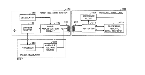
FIG. 1 generally illustrates, in block diagram form, a power
delivery system for an electronic transaction card, also referred
to as a Personal Data Card (PDC). PDC 200 is intended to be
inserted into a card reader/writer unit (receptor) designed to
transfer data to and receive data from the PDC by way of
electrical signals. PDC 200 is similar in appearance to a
conventional credit card in that it is made from an opaque plastic
3:b
material and is of approximately the same dimensions (85.7 x 54 x
0.76 mm). PDC 200 further includes the full power of a
microprocessor and associated memory - integrated circuits that
are embedded within the plastic of the card and require power in
order to operate. Although a number of techniques exist for
providing power to such circuits, the
$1.3~ t~
- 4 -
present invention discloses an apparatus and method for delivering only a
predetermined amount across a contactless interface. FIG. 1 focuses on the
power transfer from the reader/writer unit to the PDC. Aspects such as data
transfer between the PDC and the reader/writer unit are not discussed herein.
PDC 200 includes a number of circuits that require power in order to
operate and are collectively represented by block 220. Inductive device 201
includes a flexible coil and a flexible core piece. This inductive device forms a
secondary coil of a transformer which cooperates with primary coil 101 located
in power delivery system 100 of the reacler/writer unit. Rectifier 210 operates to
10 convert AC voltage into DC voltage; such rectiflers are well known among those
skilled in the art. Reference clock 230 extracts timing from the AC voltage
delivered to inductive device 201 and generates a clock signal for use by the
circuits designated 220.
The portion of the reader/writer unit that operates to power the PDC
15 comprises power delivery system 100 and power regulator 300. Power
amplification circuit 130 is driven by oscillator 110 and in turn drives primarycoil 101. Voltage is supplied to primary coil 101 in a center tapped arrangementfed from variable voltage source 320. Current monitor 120 measures the DC
current drive that flows through primary coil 101. Processor 310, among other
20 things, controls the primary voltage level, Vp, applied to the center tap of
primary coil 101 and stores in its memory the DC current drive measured by
current monitor 120.
Before PDC 200 is inserted into the reader/writer unit, processor 310
causes variable voltage source 320 to apply a sequence of stepped voltage levels25 to primary coil 101 and store in its memory the measure of a quiescent DC
current drive associated with each of the stepped voltage levels. After PDC 200
is inserted into the readerlwriter module, processor 310 causes variable voltagesource 320 to increase the voltage applied to primary coil 101 in a similar
sequence of stepped voltage levels. Thereafter, current monitor 120 measures
30 the DC current drive through primary coil 101 and presents that measurement,
in digital form, to processor 310 where it is stored in association with the
particular primary voltage that caused it to flow~ A measure of power is then
calculated from the product of these currents and voltages. For each of the
stepped voltages a power difference is also calculated between the measured
. . ' ,
13~6a~
power with and without the PDC inserted. This power difference corresponds
to the amount of power actually delivered to the PDC. When this amount
exceeds a predetermined threshold the stepping process is discontinued, and the
voltage presently being applied to primary coil 101 is fixed until the PDC is
5 removed from the reader/writer unit. ~fter removal of the PDC, new quiescent
values of power are calculated.
Referring now to FIG. 2, oscillator 110 supplies a 1.8432 M~Iz square wave
to transformer 137 through a preamplifier comprising components 131-136. In
the preamplifier, resistor 132 provides bias stabilization and sets the emitter
10 current while capacitor 133 is an associated AC bypass. The preamplifier's
square wave output is converted into a sine wave by the primary of interstage
transformer 137 which is resonated by the input capacitance of the drive field
effect transistors (FETs) 141-142, reflected back to transformer 137, and
capacitor 136 ;n parallel with the transformer primary. Resistor 135 provides a
15 fixed output impedance that prevents shorting of the tank circuit (from an ACstandpoint) when transistor 134 is on. Transformer 137 is designed to step up
the voltage by a factor of four and it is center tapped to split the output intotwo signals - 180 degrees apart.
The drive circuit of the power amplifier consists of the two FETs, 141-
20 142, arranged as a push-pull, class B amplifier. Tuning capacitors 144,14S and
resistors 143, 146 and 123 are used for wave shaping. The push-pull
configuration is used to obtain a larger peak-to-peak output swing from the
fixed supply than would be possible with a single device amplifier.
Theoretically, a peak-to-peak swing of four times the supply voltage can be
25 obtained when the output coil is resonated. Obtaining this output swing is
important because it allows the primary to have more turns for the same voltage
output at the secondary. This in turn lowers circuit Q, and consequently circuitlosses. The peak swing on each FET gate can be as high as 18 volts in the
present circuit. This swing is intentionally made high to insure that all devices
30 will turn on hard, thus reducing the variation of "on" channel resistance that
might be encountered over various devices if a low drive level is used.
FETs 141, 142 have a vt of 2 to 4 volts, and an "on" channel resistance of
2.4 ohms max. The gate drives are provided by a center tapped transformer
output, from the predrive, with the center tap DC biased at 1.8 volts nominally
~.3~36~-~. 7
to reduce deadband during transition intervals. A voltage divider comprising
resistors 138, 140 along with ~llter capacitor 139 provides the necessary bias.
Capacitors 144, 145 are used to resonate the primary coil 101. Without
defînite tuning, the primary would be excited at its self-resonant frequency and5 produce severe ringing which would create the possibility of false clock pulses
appearing on the secondary. Tuning also makes the primary circuit look like a
"real" load to the drive circuit, thus greatly reducing reactive current
components in the drive and the associated losses. The tuning capacitance is
split between capacitors 144-145, each having double the required value of
10 capacitance and placed in series across the primary halves. This provides a
smoother and more symmetrical output waveform than a single capacitor placed
across the entire primary coil 10l.
It is important to acquire a measure of the drive current flowing though
coil 101 so that an estimate of power consumption can be made. Since all
15 current that passes through the coil also passes through resistor 125 located in
current monitor 120, the DC voltage across resistor 125 is proportional to the
drive current. Resistor 125 serves as the drive current sensing resistor as well as
a source degeneration resistor for drive FETs 141, 142. The voltage across
resistor 125 is f~lltered by resistors 122, 123 and capacitor 124. Analog to Digital
20 (A/D) converter 121 is a device used to convert an analog voltage, present at its
input, into an ordered sequence of 8 binary voltages at its output. The analog
voltage referred to is, of course, the voltage across resistor 125 after ~ltering. A
clock signal of 153.6 kHz is applied to input 402 of A/D converter 121 enabling
it, in conjunction with the reference voltage on input 401, to step through a
25 series of successive approximations. Processor 310 initiates the conversion
process over leads designated ~l03. A/D converter 121 presents its output data
to processor 310 as a serial bit stream over leads 403 with the Most SignificantBit (M~B) presented first. A/D converter 121 is a conventional 8-blt seriai
converter such as the ADC 0831 available from Texas Instruments.
Processor 310 is an 8-bit microcontroller, such as the Intel 8051, that
controls A/D converter 121 and power regulator 300 to determine if an inserted
card is a PDC, and to set the power transferred to the PDC to the proper level.
Optical detectors are used to sense when a card is present and whether it is
fully inserted into the reader/writer unit. These sensor circuits are identical,
~3~
and use a slotted optical switch with mechanically activated interrupters. The
aperture dimensions of the optical switch (MST9230), used in the preferred
embodiment of the invention, are 20 mils wide by 60 mils high~ The mechanical
design insures that the aperture is either completely blocked or completely
5 opened when a card is inserted or withdrawn, respectively. Each time a card iswithdrawn from the card slot (denoted by the return of the "card in" sensor to
a high state) processor 310 enables counter 320 and sends a sequence of 15
pulses to the counter to increment the primary voltage to maximum. The drive
current that flows in primary coil 101 is measured by A/D converter 121.
10 Processor 310 then stores the value of quiescent drive current for each step of
primary voltage; quiescent power being measured when no card is inserted in
the reader/writer unit.
When the card trips the "card fully inserted" sensor, a measurement of
maximum current flow in primary coil 101 is made. Processor 310 then
15 compares this current flow with the stored value of current flow in the primary
coil without the card inserted. If the difference is greater than a predetermined
threshold, then the card is considered to be a PDC and a clamp is activated to
hold the PDC in place. The predetermined threshold is a variable, stored in
memory, that can be assigned any value.
Before clamping the PDC, processor 310 transmits one more pulse to
counter 321 which rolls it over to zero and sets the primary voltage to minimum.~fter the card is clamped, processor 310 measures the active current (l~n)
flowing in the primary coil. The value of quiescent drive current (Iq>~) for that
value of primary voltage is recalled from memory and subtracted from the value
25 obtained with the card clamped. This change in current is multiplied by the
primary voltage and by a correction factor, whose values are stored in ROM, to
determine the power being delivered to the PDC. If the calculated card power
is below a predetermined threshold (2û0 mW for example3, then the processor
increments the primary voltage, measures the drive current, repeats the
30 calculations, and again checks for proper level in the card. Once the power
being drawn by the card exceeds the predetermined threshold, processor 310
holds the primary voltage at that value until the card is removed; thereafter,
processor 310 re-measures and stores the quiescent drive current at all primary
voltage levels.
- 8 -
Counter 321 accepts pulses from processcr 310 over lines ~106 to generate
a parallel binary output signal on lines 407. An acceptable device is a 4-bit
binary counter, such as the 74LS~3, that generates sixteen different states.
Quad comparator 322 compares binary signals present on lines 407 to reference
5 voltages on lines 408 to drive four "open collector" transistor circuits at its
output. These output signals generally operate as switches between
resistors 323-326 and ground. A suitable device is the LM33~ which is available
from a number of manufacturers. A sequence ol' sixteen different voltages are
thus presented to the inverting input of amplifier 330 and compared with a
10 reference voltage present on its non-;nverting input. The reference voltage is
formed by a well-known configuration comprising series dropping resistor 501,
Zener diode 502, and filtering capacitor 503. A value of 1.235 volts is used in
the preferred embodiment. The various voltage levels emanating from
amplifier 330 ultimately control primary voltage V~ on lead 409 via pass
15 transistor 335. In the preferred embodiment, the power regulator is set to step
from 6.75 to 10.5v in equal increments. Resistor 328 provides negative feedback
to amplifier 330 and maintains bias stability. Since primary voltage Vp is
supplied to the preampli~ler as well as the power amplifier, the effect of
variations in vp are multiplied. Capacitor 337 provides filtering for vp.
Referring now to the flow chart of FIG. 3 and 4, steps are set forth that
provide the basis for a simple computer program to perform all necessary tasks
of processor 310 in controlling power delivered to the PDC in accordance with
the invention. Initiali~ation sequence 600 is designed to establish a table of
quiescent currents that flow in primary coil 101 when the PD~ is not inserted in25 the reader/writer unit.
Step 601 sets n=0. This value of n is thereafter used by the 4-bit binary
counter 321 to produce parallel binary digits "0000" at its output and ultimately
provide the minimum primary voltage level - previously selected to be 6.75 voltsin the preferred embodiment. Step 602 is the current measurement step in
30 which A/D converter 121 provides a measure of the quiescent current flow
associated with a particular value of n and is designated Iq~n-
Steps 603 and 604 set up a loop whereby 16 total values of quiescentcurrent (Iqlo~ 6) are measured and stored in a RA~v[.
Once a card is fully inserted, as indicated by a sensor on the
reader/writer unit, a maximum active current is measured (i.e., the current thatflows in primary coil 101 when vp is at its maximum level). Steps 605 and 606
perform this task. Step 607 calculates the current delivered to the card (1~) asthe difference between the maximum ac-tive current (I~ 16) and the maximum
quiescent current (1~ ,s). If this delivered current (i~) exceeds reference current
(I,CI )~ stored in memory, then it is assumed that the inserted card is a PDC;
otherwise, a magnetic stripe card (that does not draw current) is assumed.
Step 608 defines the measurement, and steps 610,611 are self explanatory.
Step 60~is invoked when it is determined that the inserted card is a
PDC - based on the delivered current calculation. The reader/writer unit may
be equipped with a solenoid that clamps the PDC in place. Step 609 causes this
to occur and simultaneously sets n=0 so that active current measurements for
various primary voltages, can be commenced. Step 612 measures and stores the
15 value of drive current (I~n) that flows in primary coil 101 for each value of n.
Step 613 calculates the power that is actually delivered to the PDC, for
each new value of n, as the product of the difference currents indicated and a
voltage Vn~ stored in ROM. This product is then multipled by a correction
factor C.F. that is experimentally determined, stored in memory, and used to
achieve correspondence between mathematical calculations and actual power
measurements. The correction factor is a system constant that accounts for
inherent measurement inaccuracies, flux leakage, etc.
When the power delivered to the PDC exceeds a predetermined
threshold, stored in ROM, steps 615-816 provide an indication that data
transfer between the reader/writer unit and the PDC may commence until the
card is removed. If, howeverS the power delivered to the PDC is less than the
predetermined threshold~ step 617 increases the value of n, hence the primary
voltage, and repeats the measurements of steps 612 and 613.
In the event that the power being delivered to the PDC is still less than
30 the predetermined threshold after the maximum primary voltage is applied,
steps 618 and 619 provide a default state whereby a maglletic stripe card is
assumed. Normally, step 610 would have detected this condition.
~3rl~6(:~G)7
- 10-
When the card is removed, initialization sequence 600 is repeated to
accommoclate any drift in quiescent currents from day to day due to equipment
wear, temperature variation, and unforeseen changes.
The above-described invention thus provides a method and apparatus for
5 delivering a predetermined amount of power to a PDC. Advantageously, power
regulation is accomplished within the card reader/writer unit so that regulator
circuits and their associated power dissipation are eliminated from the PDC
itself. As an added advantage, monitor;ng the amount of power transferred
provides an ability to distinguish between various types of cards (e.g., PDC or
10 conventional credit cards). This is useful in two ways: (i) it provides an ability
to be compatible with conventional credit cards and (ii) it provides a means fordistinguishing among future "smart cards."
Although power regulation is well known, the present invention provides
a unique way in which to achieve it across a contactless interface; and while a
15 specific embodiment is disclosed, it is understood that various modifications are
possible within the spirit and scope of the invention. One modification being
the elimination of quiescent current measurements each time a card is removed
from the reader/writer unit. Instead, estimates of quiescent current are stored
in memory that have been selected as representative of the particular
2n reader/writer unit design. Another modification being the elimination of the
microprocessor and digital memory. Instead, an analog Leedback circuit,
responsive to current flow in the primary coil, is used to control the variable
vol$age source. System parameters that are expected to exhibit minimum
variation over the lifetime of the reader/writer unit, such as quiescent currents,
25 are accommodated by adjustable components in the feedback circuit that are
~lxed at the time of manufacture.