Note: Descriptions are shown in the official language in which they were submitted.
~3060~2 FJ-7094
~ 1 --
DIGITAL SIGNAL PROCESSING SYSTEM IN A MODEM
BACKGROUND OF THE INVENTION
1. Field of the Inv~ention
The present invention relates to a digital
signal processing system provid~d in a modulator/
demodulator (below, modem) in a digital data trans-
mission network. More particularly, it is relates to a
digital signal processing system for compensating a base
band signal or pass band signal received in the modem
using a predetermined sampling frequency.
An output of the digital signal processing
system is supplied to a personal computer, a facsimile
apparatus and the like through the digital data
transmission network.
2. Description of the Related Art
A digital signal processing technique is
widely utilized in the field of information processing.
In general, first, a digital signal is converted to a
base band signal based on a Nyquist rate, second, the
base band signal is wave-shaped by a filter and also
2~ converted to a pass band signal based on a modulation
method in the modem, third, the pass band signal is
transmitted to another modem through the analog or
digital data transmission network, fourth, the pass band
signal is converted to the original base band signal
(demodulation), and last, the base band signal is
recovered in the other modem.
~ he modem mainly has two functions, i.e., the
modulation and demodula*ion as explained above.
Furtherl the type of the modem can be classified into
high speed modems and low speed modems based on the
processing speed. Low speed modems are mainly used for
frequency shift keying (FSK) at a data transmission
speed lower than 1200 bps (bit per second). While, high
speed modems are mainly used for a phase shift keying
(PSK) or a quadrature amplitude modulation (QAM) at a
~ .
~3~ 2
data transmission speed higher than 2400 bps.
In the demodulation process, it is necessary
to compensate phase jitter distortion contained in the
pass band signal, particularly, in a low speed modem.
One example of a digital signal processing
system, "an automatic equalizing method and system" by
Noriaki Fujimura, is disclosed in U.S. Patent
No. 4,097,807. This methocl is used for a suppressed
carrier data transmission system for automatically
compensating amplitude for s~atic and dynamic variations
in the phase, delay and frequency characteristics of a
transmission channel in a high speed data transmission.
As an another example, ~Joint Equalization and
Carrier Recovery Adaptation in Data Transmission
Systems" by Falconer is disclosed in U.S. Patent
No. 3,878,468. This prior art shows a pass band system
and base band system. Both pass band and base band
systems can be adapted to a low frequency system as
- mentioned above.
2 0 SUMNARY OF THE INVENTION
The object of the present invention is to provide a
reception signal processing system which can operate at
the low frequency for suppressing the phase jitter
caused by a power source.
The another object of the present invention is;to
provide a digital signal processing system in a modem
~or enabling suppression of phase jitter at high
frequencies contained in a base band signal or pass band
signal when the received signal is processed in the
modem by using a predetermined sampling frequency the
same as a baud-rate frequency or a frequency higher than
the baud-rate frequency.
In accordance with the present invention, there is
provided a reception signal processing system in a
communication system transmitting a data under a
predete~nined baud-rate, including: a first unit
operated by a first frequency for inputting the
z
-- 3 --
reception signal and for recovering loss components in
the reception signal; a second unit operatively
connected to the first unit and for responding to an
output of the first unit, for determining a first ideal
reception signal corresponding to the output of the
first unit based on a second frequency corresponding to
the baud-rate, and the first frequency being higher than
the second frequency; and a third unit operatively
connected to the first unit and second unit for
responding to the.first ideal reception signal from the
second unit based on the frequency and for generating
and providing a second ideal reception signal based on
the first frequency to the first unit; the second ideal
reception signal being deriv~d by processing the first
ideal reception signal based on the first frequency, and
the first ideal reception signal corresponding to the
data transmitted.
Further, a digital signal processing system in a
modem, including: an equalization circuit operated by a
predetermined sampling frequency for compensating an
amplitude and a delay distortion of a base band signal
demodulated from a reception signal or pass band signal
in the modem; a carrier phase control circuit
operatively connected to the equalization circuit and
operated by the predetermined sampling frequency for
correcting a phase shift of the base band signal; a
decision circuit operatively connected to the carrier
phase control circuit and operated by a predetermined
baud-rate frequency for generating decision data from
the base band signal; a frequency conversion circuit
operatively connected to the decision circuit for
converting a sampling frequency of the decision data to
the predetermined sampling frequency; and a calculation
circuit operatively connected between the carrier phase
control circuit and the decision for obtaining a
difference signal between an output of the frequency
conversion circuit and an output of the carrier phase
~3~6~
-- 4
control circuit, the diff0rence signal being fed back to
the equalization circuit and the carrier phase control
circuit so that the difference signal becomes zero.
Still further, in one aspect of the present
invention, the frequency conversion circuit comprises:
a delay element for delaying the decision data and
outputting delayed decision data, the decision data
obtained from the base band signal demodulated from the
reception signal having a :roll-off rate of 100%; a
second decision circuit fo:r inputting the decision data
and the delayed decision data, obtaining an intermediate
point between present decision data and delayed decision
data just befoxe the present decision data, and
outputting intermediate decision data; and a switching
circuit for switching between the decision data and the
intermediate decision data, and obtaining a signal of
twice the baud-rate frequency used as a sampling signal
having the predetermined sampling freguency.
^ Still furthex, in another aspect of the present
invention, the frequency conversion circuit comprises an
interpolator for generating a sampling signal having the
predetermined sampling frequency based on the decision
data.
BRIE:F DESC~IPTION OF THE DR~WINGS
In the drawings:
Fig. 1 is a schematic block diagram of a
conventional digital signal processing system provided
in a modem,
Fig. 2 is a basic block diagram of a digital
30 signal processing system according to the present ~ -
invention;
Fig. 3 is a schematic block diagram of a
digital signal processing system according to an
embodiment of the present invention;
Fig. 4 is a view for explaining an inter-
mediate point of an impulse response curve;
Figs. S and 6 are curves for explaining a
~3C)~
roll-off rate;
Fig. 7 is a view for explaining a sampling
frequency having a double baud-rate frequency;
Fig. 8 is a schematic block diagram of a
digital signal processing system according to another
embodiment of the present invention;
Fig. 9 is a view for explaining a difference
signal output from a calculation circuit shown in
Figs. 2, 3 and 8;
Fig. 10 is a detail block diagr~m of an
interpolator shown in Fig. 8;
Fig. 11 is one example of a zero insertion
circuit shown in Fig. 10;
Fig. 12 is a view for explaining the relation-
ship between decision data and a switch signal;
Fig. 13 is one example of a roll-off filter
shown in Fig. 10 r
Fig. 14 is a view for explaining a filtered
- signal In shown in Fig. 13;
F.ig. 15 is one example of an equalization
circuit shown in Figs. 2, 3 and 8;
Fig. 16 is one example of a carrier phase
control circuit shown in Figs. 2, 3 and 8; and
Fig. 17 is a one example of a decision circuit
shown in Figs. 2, 3 and 8.
DESCRIPTION OF THE PREFERRED EMBODINENTS
Before describing the preferred embodiments, the
explanations will be given of a conventional digital
signal processing system and problems thereof.
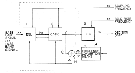
Figure 1 is a schematic block diagram of a conven-
tional digital signal processing system provided in a
modem. In Fig. 1, 11 denotes an equalization circuit
(EQL), 12 a carrier phase control circuit (CAPC), 13 a
decision circuit and 14 a calculation circuit. Further,
Xn is a base band signal or pass band signal input into
the equalization circuit 11.
The equalization circuit 11 compensates an
~3L16~:LZ
-- 6
amplitude and a delay distortion of the base band signal
or pass band signal XII demodulated in the modem, and
outputs an equalization signal Hn. One example of the
equalization circuit ll is shown in Fig. 15. The
carrier phase control circuit 12 receives the
equalization signal Hn ancl corrects a phase shift of the
equalization signal Hn ancl outputs a correction
signal Yn. One example of the carrier phase control
circuit 12 is shown in Fig. 16.
The decision circuit 13 receives the correction
signal Yn, extracts the data from the correction signal
Yn and outputs decision data Rn. The calculation
circuit 14 receives the decision data Rn, and calculates
a difference signal between a baud-rate frequency fb
corresponding to the decision data Rn and the correction
signal Yn. The difference signal ~ between the signal
Rn and the signal Yn is fed bac~ to the equalization
circuit 11 and the carrier phase control circuit 12 so
-~ that the difference signal becomes zero.
The digital signal processing system shown in
Fig. 1 is generally operated in accordance with the
baud-rate frequency fb input into the equalization
circuit 11, the carrier phase cQntrol circuit 12, the
decision circuit 13 r and the calculation circuit 14.
In the low speed modem, for e~ample, the frequency
150 Hz is used as the band-rate frequency of the trans-
mission in V.34 of the CCITT recommendation.
Accordingly, when the sampling frequency for the base
band signal Xn to the equalization circuit ll and the
carrier phase control circuit 12 is equal to ~he baud
rate frequency fb (for example, fb = 150 ~z), it is
possible to only suppress the phase jitter generated
under 75 Hz because the carrier phase control circuit 12
operates in accordance with the baud-rate frequency fb
as the sampling frequency. While, in the high speed
modem, it is possible to suppress the phase jitter at
very high frequencies because the sampling frequency
~3~ 2
-- 7
applied to the carrier phase control circuit 12 is very
high.
Phase jitter also occurs at double or three times
of the frequenc~ (100 Hz or 150 Hz) of a power source
frequency (for example, 50 Hz) in the low speed modem.
However, the phase jitter at the above frequencies
cannot be suppressed because half of the sampling
frequency is under 75 Hz.
Figure 2 is a basic block diagram of a digital
signal processing system according to the present
invention. In Fig. 2, reference number 1 denotes an
equalization circuit, 2 a carrier phase control circuit,
and 3 a decision circuit. Reference number 4 denotes a
frequency conversion means according to the present
lS invention for converting the sampling frequency of the
decision data Rn to the higher frequency used as the
sampling frequency.
In this system, although the equalization circuit 1
~ and the carrier phase control circuit 2 are operated by
the sampling signal having the frequency fs, the
decision circuit 3 be operated by the baud-rate
frequency fb. Accordingly, it is necessary to convert
the frequency of the decision data Rn to the sa~pling
frequency fs to obtain the difference signal ~ and feed
~ack the difference signal ~ to the equalization
circuit 1 and the carrier phase control circuit 2. The
sampling frequency in this system can be converted to a
frequency at least double the baud~rate frequency as
explained hereinafter.
Figure 3 is a schematic block diagram of a digital
signal processing system according to an embodiment of
the present invention. In Fig. 3, the frequency
conversion means is constituted by a second decision
circuit 41 for obtaining a frequency double the baud-
rate frequency fb as the sampling frequency fs, a delay
element (T) 42 having a register for delaying decision
data Rn, and a switching device 43 for switching the
~3~6a!~
-- 8 --
decision data Rn and an intermediate decision data Rd
and obtaining the sampling signal having a frequency
double the baud-rate frequency fb. In this case, the
frequency conversion means 4 of this embodiment is
applied to the base band c;ignal Xn demodulated from the
reception signal having a roll-off (ROF) rate of 100%.
The operation of the digital signal processing
system according to the present invention is explained
in detail hereinafter.
In Fig. 3, the decisi.on circuit (DEC(1)) 3
generates the decision dat;a Rn after deciding the
correction signal Yn. The decision of the correction
signal Yn in the decision circuit 3 i5 performed by
; comparing an ideal point of reception with a reception
point corrected by the carrier phase control circuit 2
on a complex coordinate.
The decision circuit ~DEC(2)) 41 in the frequency
conversion means 4 calculates an intermediate point A
- (see, Fig. 4) between the decision data Rn from the
decision circuit 3 and the before decision data Rt
delayed by th~ delay element 42 as explained in detail
in Fig. 4. The switching device 43 generates the
sampling signal Sn having a dou~le baud-rate frequency
by alternately switching the decision data Rn and the
intermediate decision data Rd. The sampling signal Sn
is input into the calculation circuit 14 and the
difference signal Q between the correction signal Yn and
the sampling signal Sn is fed back to the equalization
circuit 1 and the carrier phase control circuit 2 so
that the difference signal becomes zero. ~ccordingly,
it is possible to compensate the amplitude and delay of
the base band signal Xn demodulated from the reception
signal, and to correct the phase distortion in the
equalization circuit 1 and the carrier phase control
circuit 2 based on the difference signal ~.
Figure 4 is a view for explaining the intermediate
point of the impulse response curve. "P2" denote the
~306~1Z
g
point of the present decision data Rn and "Pl" denotes
the point just before decision data Rn. "A' denotes the
intermediate point and "P" an amplitude. The point A is
located at half of the amplitude P. The sampling
frequency fs having a double baud-rate frequency can be
obtained by switching the switching device 43 as
explained below.
Figure 5 and 6 are curves for explaining the
roll-off rate (ROF)o The roll-off rate ROF can be
expressed by following formula.
ROF = (~/1 x 100%)
where, ''1" is a frequency from ''0'l to ~fc~ (fc denotes a
half amplitude point), and ~ is a difference frequency
from "fl" to ~fc" (fl denotes a trailing edge of the
amplitude curve). Accordingly, when the interval "1" is
equal to the interval ll~ll as shown in Fig. 6, the
roll-off rate ROF becomes 10Q% based on the above
formula. Each of the impulse response curves shown in
- Fig. 4 has a roll-off rate of 100~.
Three roll-off filters are provided in the system.
That is, the first roll-off filter (ROF 1) is provided
in the transmission system. The second roll-off filter
(ROF 2) is provided for the inner or previous stage o~
the equalization circuit l in the reception system. The
third roll-off filter (ROF 3) is provided in the
interpolator shown in Fig. 8. The relationship among
these roll-off filters is given by;
ROF 1 x ROF 2 = ROF 3
Figure 7 is a view for explaining the sampling
frequency of double the baud-rate frequency. The
waveform (A) denotes a baud-rate frequency fb, for
example, fb = 150 Hz. The baud-rate frequency fb is
expressed by a reciprocaI of a modulation rate. (B)
denotes digital data train to be transmitted at the
baud-rate frequency fb. (C) denotes impulse response
curves each having a roll-off rate of 100%, corre-
sponding to the digital data. (D) denotes a curve
~L386(:)~2
-- 10 --
obtained by the connection of each of the point of the
decision data from the decision circuits 3 and 41. (E)
denotas the resultant digital data from each decision
circuits 3 and 41. The data Rn is obtained from the
decision circuit 3 and the data Rd from the decision
circuit 41. (F) denotes the sampling frequency fs
obtained from the data Rn and Rd. As is obvious, the
sampling frequency fs is given by a frequency double the
baud-rate frequency fb shown in (A).
As explained above, in this embodiment, the base
band signal demodulated from the reception signal or
pass band signal having a roll-off rate of 100% can be
processed b~ the sampling signal fs having a double
baud-rate frequency fb. Accordingly, it is possible to
easily suppress the phase jitter caused by the doublin~
of the power source frequency, based on the higher
sampling frequency than the baud-rate frequency.
Figure 8 is a schematic block diagram of a digital
- signal processing system according to another embodiment
of the present invention. In Fig. 8, the frequency
conversion means 4 of this embodiment is constituted by
an interpolator 44. The frequency conversion means 4 of
this embodiment is applied to t~e base band signal
demodulated from the reception signal regardless of the
previous roll-off filters (ROF 1) and (ROF 2). The
interpolator 44 operates as a filter and generates a
sampling frequency higher than the baud-rate frequency
by multiplying the decision data Rn from the decision
circuit 3. The calculation circuit 14 calculate the
difference signal between the correction signal Yn and
the output In from the interpolator 44, and the
difference signal ~ is fed back to the equalization
circuit 1 and the carrier phase control circuit 2 so
that the difference signal becomes zero.
Figure 9 is a view for explaining the difference
signal Olltput from the calculation circuit 14 shown in
Figs. 2, 3 and 8. In FigO 9, the ordinate is an
imaginary part, and the abscissa is a real part. The
reference letter In is the output of the interpolator 44
and Yn is the output of the carrier phase control
circuit 2. The symbol ~ is the difference signal
between the output In and the output Yn. It is
necessary to reduce the difference signal by feeding
back the difference signal to the equalization circuit l
and the carrier phase control circuit 2.
Figure 10 is a detail block diagram of the
interpolator shown in Fig 8. In Fig. 10, 441 is a zero
insertion circuit, and 442 is a roll-off filter. The
zero insertion circuit 441 receives the decision data Rn
from the decision circuit 3, and outputs a switch
signal Pn. The roll-off filter 442 receives the switch
signal Pn, and outputs a filtered output In.
Figure ll i6 one example o~ the zero insertion
circuit, and Figure 12 is a view for explaining the
relationship between the decision data Rn and the switch
signal Pn. In Fig. ll, the zero insertion circuit is
~ constituted by a switching means SW having a plurality
of terminals corresponding to the sampling number. When
the switch is positioned at the terminal 1, the decision
signal Rn is output from the circuit 441 as the switch
signal Pn. When the switch is switched to other
positions, the switch signal Pn becomes 'lOIl as shown in
Fig. 12.
Figure 13 is one example of the roll-off
filter 442, and Figure 14 is a view for explaining the
filtered signal In. In Fig. 13, the roll-off filter 442
is constituted by a transversal type filter. The switch
signal Pn is input into a first delay element T/m, and
transferred sequentially after a predetermined delay
time at each delay element T/m. Qk is a coefficient of
the roll-off filter, and coefficient Qk is multiplied by
each out.put of the delay element T/m. The filtered
signal l.n is given by the sum of the multiplication
Qk x Pn - k. In Fig. 14, T is a baud-rate period, and
~30fi~Z
- 12
T/m is a sampling rate. For example, when the baud-rate
period is 2400 bps and the sampling rate is 9600 bps,
T/m is given by T/4. Accordingly, m/T denotes the
sampling frequency. The curve shown in Fig. 14 shows
the filtered signal In at each coefficient Qk.
Figure 15 is one example of the equali~ation
circuit 1 constituted by the transversal type filter
having a shift register. This circuit is mainly used
for compensating the signal delay distortion and the
amplitude distortion on the line. The base band signal
or pass band signal Xn is input to the delay element
t/m, and the input signal is sequentially transferred
after the predetermined delay in each delay elemenk T/m.
Ck is a tap coefficient at each delay element and
multiplied by each output of the delay element T/m. The
equalization signal Hn is given by the result of the
multiplication Ck x Xn - k. In this case, Co is a
center tap.
- Figure 16 is one example of the carrier phase
contro~ circuit for correcting the phase shift of the
carrier. The equalization signal Hn is multiplied by
the coefficient ejon, and outputs the correction
signal Hn.
Figure 17 is one example of the decision circuit 3.
In Fig. 17, the decision circuit 3 is constituted by a
read only memory ROM having a predetermined table. The
decision data Rn is stored in the table.