Note: Descriptions are shown in the official language in which they were submitted.
~3~6~
FIELD OF TE[E INVh'NTIO~
The present invention relates generally to the
field of ultrasonic imaging, and more particularly to
ultrasonic imaging to determine various character-
istics of relatively small cavities and surrounding
structures.
~AC~GROUND OF TH~' INVENTION
In the United States and many other countries,
heart disease is the leading cause of death and
disability. One particular kind of heart disease is
atherosclerosis, which involves the deposition of
fatty material on the inside of vessel walls
throughout the body (commonly called "plaque"). As
the plaque collects, the artery narrows and blood
flow is restricted. If the artery narrows too much,
the heart muscle nourished by the artery receives
insufficient oxygen and a myocardial infarction sr
"heart attack" can occur. Atherosclerosis can occur
throughout the human ~ody, however, it is most life
threatening within the coronary vasculature.
Physicians have a wide range of tools at their
disposal to treat patients with coronary artery
diseas2. Coronary artery bypass grafts or "open
heart" surgery can be performed to bypass blocked
artery segments. Other, less invasive procedures are
available. For example, some blockages may be
dissolved by chemical treatment. Alternatively, a
procedure known as percutaneous transluminal coronary
angioplasty (hereinafter "PTCA") may be performed in
which a catheter with an expandable section on its
end is placed within the narrowed artery and inflated
to compact the plaque against the vessel wall,
thereby relievin~ the blockage.
39-142/mld
s~
No matter what method is used to treat coronary
artery disease, it is necessary Eor physicians to
obtain quantitative information on the condition of
the vasculature within the heart. Traditionally,
coronary angiography has been the method of choice.
Coronary angiography involves the placement of the
end of a catheter at the beginning of the coronary
vasculature. A small amount of radiopaque dye is
injected, and a X-ray motion picture is taken while
the dye is pumped through the vessels. ~he phy~ician
then examines the pictures and looks for any telltale
narrowing of the blood flow opacified by the
radiopaque dye. By the number and degree of such
narrowing, the course of treatment can be determined.
Angiography has the extreme li~itation of
indicating only where the blood is within the vessel;
it reveals nothing of the condition of the inside of
the vessel and the vessel wall itself. Furthermore,
most angiography machines present virtually only one-
dimensional projections of where blood flow exists.
Because of this imaging limitation, the complex
structures within the coronary vasculature often
exhibit quite ambiguous images.
Recently, imaging of soft tissue such as gross
cardiac structures has provided physicians with
diagnostic images having quality that is unavailable
from conventional techniques using X-ray radiation.
In particular, magnetic resonance imaging (MRI) and
ultrasound have become important diagnostic tools for
cardiac assessment. Although MRI has the ability to
image blood vessels, the image resolution is not
sufficient to allow assessment of the condition of
the walls of the vessel. Conventional ultrasound
scanning also suffers from lack of resolution. More
recently, high frequency (hence, high resolution)
--2--
39-142~mld
~3~6~SO
ultrasound has been used during open heart surgery to
access the coronary arteries. This method requires
the opening of the chest cavity to expose the heart
surface and is hence limited in its application.
In an even more recent development, in vivo
ultrasonic imaging of the human body creates the
potential for access to a wealth of information
regarding the condition of a patient's vasculature
that is currently only at best indirectly available
from other sources. The inforxnation received from in
vivo imaging may be used as a diagnostic tool to help
determine patient treatment, or as a surgical tool,
supplementing angiography in PCTA.
In vivo ultrasonic imaging from within the heart
has been described in U.S. Patent No. 3,9S8,502 to
Bom. In order to provide for ultrasonic imaging
inside the human body, the Bom patent provides an
array of small transducer elements which may be
introduced into the body by way of catherization.
The array of elements is excited at ultrasonic
frequencies and the reflections or echos of the
generated ultrasonic acoustic waves are detected by
the piezoelectric properties of the transducers.
Unfortunately, due to the nature of the material used
for the transducers, the array of elements cannot be
made small enough to allow passage into small areas
such as the coronary arteries. Therefore, use of the
Bom device is limited to within the heart chambers
and the associated great arteries.
An additional limitation of the Bom device i5
the poor resolution caused by a sparse distribution
of transducer elements. Piezoeletric materials of
the type used by Bom (e.g., ceramics) have a
practical limitation in size reduction. Because of
39-142/mld
~l3~36q~
this size limitation and the fact that the maximum
resolution of the transducer array is limited by the
center-to-center spacing of adjacent elements~ the
Bom device is inherently limited in the quality of
its image resolution.
A further limitation of the Bom device is the
fixed delays it provides for focusing an image. Such
fixed delays do not provide satisfactory images for
identification of tissue structures. For a
satisfactory image, a dynamic focusing feakure is
needed to provide an optimal i-ocus at a plurality of
points in the imaging plane. One approach to
implementing such a dynamic focusing feature is a so-
called "synthetic focus" or "synthetic-aperture"
approach disclosed in U.S. Patent No. 4,325,257 to
Kino et al.
For many diagnostic and therapeutic purposes, in
vivo ultrasonic imaging must simulate real-time
performance. To achieve diagnostic or therapeutic
quality images in small cavities while maintaining
real-time performance is a formidable ta~k and one
which applicants believe has not previously been
attained.
5UMMARY OF T~E INVENTION
It is a general object of the invention to
provide diagnostic quality, virtual real-time
ultrasonic images of small cavities and their
associated surrounding structures from within the
cavities.
It i5 a further object of the invention to
provide a method of providing diagnostic quality,
virtual real-time ultrasonic images that is
sufficiently flexible to accommodate a range of
39-142/mld
5~
ultrasonic imaging requirements from within small
cavities.
It is a further object of the invention to
provide an array of transducer elements for
generating ultrasonic imaging clata that is small
enough to enter small cavitiesl yet also exhibit
controlled behavior and is manufacturable on a
commercial basis. In this connection, it is a
related object of the present ;Lnvention to maintain a
high degree of sensitivity to signals from weak
reflectors of ultrasonic signals, such as human
vascular tissues, while maintaining the small size of
the array of transducers.
It is another object of the invention to provide
the physician with the ability to accurately position
the array of transducers within the imaging area.
It is yet another object of the invention to
minimize the number of wires required to connect the
in vivo portion of the ultrasonic imaging device of
the invention to an in vitro processing stage. In
thi~ connection, it is a related object of the
invention to distribute the control of the excitation
of the array of transducer elements between in vivo
and in vitro sites.
It is still another object of the invention to
electrically isolate the in vivo portion of the
imaging device of the invention in order that it is
safe for use in human imaging applications~ In this
connection, it is a related object of the invention
to provide operation of the imaging device without
causing ~ignificant risk to humans from excessive
localized heating or radiation.
A still further object of the present invention
is to operate at very low power dissipation in vivo
--5--
39-142/mld
~.3[)6~
in order to prevent heating of ~urrounding tissue and
expansion of parts.
It is a further object of the present invention
to provide an imaging device whose in vivo portion
may be mounted to a positioning device such as a
catheter, which allows the use of, for example,
conventional guiding catheterc; and guidewires. In
this connection, it is a related object of the
present invention that the imaging device be suitable
for incorporation into recent catheter systems, and
allowing for the continued use of, for example,
guiding catheters and guidewires, in conjunction with
catheter-based diagnostic and therapeutic procedures
such as angioplasty, regional therapy for dissolving --
plaque and the like.
It is a more detailed object of the invention to
provide an in vivo imaging device for producing real-
time images of small, moving or stationary cavities
and surrounding tissue structure that is uniquely and
advantageously constructed using a conventional
catheter assembly fitted at its end with a probe
assembly for transmitting and receiving ultrasonic
signals from elements of an array of ultrasonic
transducers incorporated into the probe assembly.
The transducer elements are selected and controlled
by an in vitro electronic signal processing and
imaging unit which transmits excitation and control
signals via a transmission cable to integrated
circuitry on-board the body of the probe assembly.
The integrated circuitry routes excitation signals to
the transducer elements in a predetermined
sequence. The body of the probe assembly not only
supports the array of transducer elements and the
integrated circuitry, but also accommodates
conventional catheter devices such as a catheter
39-142/mld
~3~6~350
guidewire that may ~e threaded through the probe
assembly.
The number of wires in the transmission cable
connecting the integrated circuitry to the proce~sing
and imaging unit are minimized by providing for
multiplexing task at the integrated circuitry on-
board the probe assembly. Due to the relatively few
number of conductors comprising the transmission
cable, there is a high degree of physical flexibility
achieved, and there is a relatively small cross-
section obtained, which makes the device convenient
for use within the limited confines of its intended
operating environment. The integrated circuits also
buffer excitation signals from the transmission cable
which are directed to a selected element in
accordance with a preferred image reconstruction
scheme. These pulses are converted into ultrasonic
waves by the transducer elements. The echoes or
reflections from the environment are received by the
transducer elements, converted back into electrical
signals which are relatively weak, and buffered by
the integrated circuit~ so that the weak signals are
boosted before being directed onto the transmission
cable for delivery to the signal processing and
imaging unit.
Because of the very small size of the probe
assembly, the piezoelectric material used for the
array of transducer elements is preferably continuous
in order to simplify construction of the probe.
Further, the material may be characterized by a high
inter~al electrical impedance resulting in weak
electrical output current in response to ultrasonic
echos. In order to provide a wide beam pattern as
desired by the preferred imaging technique, the
transducer elements adjacent an element or elements
39-142/mld
so
receiving an excitation signal are shunted to a low
impedance to confine the active region to the
selected transducer or transducers.
Within the electronic signal processing and
imaging unit, signals indicative of the reflections
or echos of ultrasonic acoustic waves are processed
at extremely high speeds such that signal digiti-
zation and dynamic digital signal averaging, with
respect to each individual or group of transducer
elements, may be implemented, l:hereby producing
resultant signals having a very high dynamic range.
These resultant signals are then processed into
diagnostic information in the form of, for example,
images. The signals are preferably processed using a
synthetic-aperture approach wherein dynamic time
delays and weighting factors are used to produce a
myriad of individually focused points throughout the
entire image plane, thereby resulting in real-time,
high resolution diagnostic images of the cavity and
surrounding structure.
E~RIEl? DESCRIPTION OF TEIE DRAWINGS
Other objects and advantages of the invention
will be apparent from the following detailed
description and the accompanying drawings, in which:
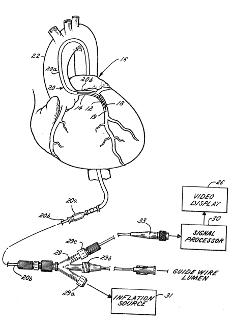
FIGURE 1 is a system-type diagram of the ultra-
sonic imaging device of the invention, illustrating
the use of the device to image a coronary artery
during a PTCA procedure;
FIG. 2 is an enlarged and partially sectioned
view of a portion of the coronary artery in FIGURE 1,
showing the probe assembly of the ultrasonic imaging
device of the invention located at the tip of the
catheter approaching an area o plaque buildup in the
--8--
39-142/mld
9L3~6~SO
artery and the equivalent histologic view of the same
to a surgeon;
FIG. 3 is the same view as illustrated in
FIG. 2, except the catheter has been further drawn
into the area of plaque buildup in the coronary
artery so as to bring a balloon section of the
catheter into the area, where the balloon is inflated
in order to compress the plaque in accordance with a
standard PTCA procedure;
FIG. 4 is the same view as illustrated in FIGS.
2 and 3, except the catheter has been repositioned so
that the probe assembly of the ultrasonic imaging
device is in the area of the plaque buildup, and it
is providing the surgeon with an image of the cross-
sectional area of the coronary artery that can be
used to determine how well the PTCA procedure opened
the artery for additional blood flow;
FIG. 5 is a cross-sectional view of the tip of
the catheter in FIGS 2-5, illustrating the probe
assembly of the ultrasonic imaging device of the
invention housed in the tip of the catheter and
adjacent to its balloon section;
FIG. 6 is perspective view of the probe assembly
of FIGS. 2-5 with the sheath and epoxy encapsulation
covering the probe assembly removed to expose the
underlying electronics and associated construction;
FIG~ 7 is cross-sectional view of the probe
assembly taken along the line 7-7 in FIG. 6;
FIG. 8 is a side view of the probe assembly with
a portion cut away to expose the composition of the
body of the assembly along its longitudinal axis;
FIG, 9 is a graph illustrating an exemplary
fre~uency spectrum echo response for one of the
_9_
39-142/mld
~.3~6~SC~
transducer elements defined by a conductive .trace on
the probe assembly and an overlying portion of a band
of a piezoelectric polymer/ where the abscissa is the
frequency of the acoustic waves impinging on the
transducer element measured in Megahertz and the
ordinate is the electrical res]ponse of the piezo-
electric polymer measured in m.icroamps,
FIG. 10 is a graph similar to that of FIG. 9,
except the frequency response of the transducer
element is measured after it has been converted by a
transimpedance amplifier configuration incorporated
in integrated circuitry on-board the probe assembly,
where the abscissa is still measured in megahertz but
the ordinate is now measured in volts;
FIG. 11 is a schematic block diagram of the
electronic circuitry contained in each of the
plurality of chips mounted to a carrier portion of
the probe assembly;
FIG. 12 is a detailed component diagram of a
delay buffer which provides important timing signals
in the electronic circuitry of FIG. 11;
FIGS. 13a and 13b illustrate a schematic block
diagram of the in vitro processing and imaging unit
of the ultrasonic imaging device according to an
exemplary embodiment of the invention;
FIG. 14 is a diagrammatic representation of a
portion of the array of acoustic transducers and one
of a plurality of radial focus beams, each having a
plurality of focus points for reconstructing an image
derived from partial vectors associated with the
ultrasonic signals received by the transducers;
FIG. 15 is a schematic illustration of the
screen of a video display used to generate the images
--10--
39-142/mld
~3~S~
shown in FIGS. 2 and 4, showing how the plurality of
radial focus beams are mapped onto the pixels of the
screen; and
FIG. 16 is an enlarged and partial view of the
schematic in FIG. 15, illustrating how the points
comprising the focus beams are matched with the
pixels of the video display screen;
FIG. 17 is a graph in Cartesian coordinates of
an exemplary beam profile for leach element in the
transducer array, where the normalized amplitud~ as
plotted on the ordinate is mea~ured at a constant
radius and the beam angle plotted on the abscissa is
measured from the center of the cylinder formed by
the array;
FIG. 18 is a graph in Cartesian coordinates of
the Hamming window profile for a single element in
the transducer array, where the normalized amplitude
is plotted on the ordinate and a circumferential
distance from a central radial beam is plotted on the
abscissa .
While the invention will be described in
connection with angioplasty or PTCA surgery, it will
be understood that it is not intended to be limited
to such use, On the contrary, the invention is
intended to cover all applications which may require
imaging in a small cavity. An example of such an
alternative application is the use of the invention
on the end of a catheter without the incorporation of
a balloon. A specific example of such a use is a
pharmaceutically therapeutic use where cholesterol-
inhibiting drugs are used for regional therapy and
the imaging device of the invention is used to
monitor the effectiveness of the drugs in rPmoving
plaque. Another specific example of an alternative
39-142/mld
use is a physical therapeutic use such as measuring
blood flow rates (using Dopler sound imaging in
conjunction with invention) or determining sizes and
locations of gall stones and the like. Yet another
example of an alternative application is the
incorporation of the invention into a catheter in
conjunction with a laser or like devices for burning
plaque in the arteries.
DETAILED DESCRIPTION OF THE PREFERRED EMBODIMENT
Turning to the illustrated embodiment and
referring first to FIGS. 1-4, a buildup of fatty
material or plaque 12 in a coronary artery 14 of a
heart 16 may be treated in certain situations by
inserting a balloon 18, in a deflated stater into the
artery via a catheter assembly 20. As illustrated in
FIGURE 1, the catheter assembly 20 is a three-part
assembly, having a guide wire 19, a guide catheter
20a for threading through the large arteries such as
the aorta 22 and a smaller diameter catheter 20b that
fits inside the guide catheter. After a surgeon
directs the guide catheter 20 and the guide wire 19
through a large artery leading to the aorta 22, the
smaller catheter 20b is inserted. At the beginning
of the coronary artery 14 that is partially blocked
by the fatty material 12, the guide wire is first
extended into the artery, followed by catheter 20b,
which includes the balloon 18 at its tip.
Once the balloon 18 has entered the~coronary
artery 14, an ultrasonic imaging device including a
probe assembly 24 housed in the tip of the catheter
20b provides a surgeon with a cross-sectional view of
the artery on a video display 26. Signals from the
probe assembly 24, indicative of reflected ultrasonic
waves, are transferred along a cable 28 to a signal
39-142/mld
~3~ S~
processor 30 located outside the patient. The
catheter 20b ends in a three-port junction 29 of
conventional construction that couples the catheter
to an inflation source 31, a guide wire source and
the signal processor 30. The inflation and guide
wire ports 29a and 29b, respect:ively, are o~
conventional PTCA catheter construction. The third
port 29c provides a path for the cable 28 to connect
with the signal processor 30 and video display 26 via
an electronic connector 33.
As previously noted, the invention is not
intended to be limited to a PTCA environment. In
this regard, it will be appreciated that for use of
the invention in a regional therapy application where
cholesterol-inhibiting drugs are used, the port 29a
may be an injection site for the drug instead of an
inflation source and, of course, the balloon 18 at
the end of the catheter 20b is not needed.
Returning to a discussion of the invention in a
PTCA application, the imaging device provides an
image 32 on the display 26 that indicates wh-en the
balloon 18 is within a partially blocked area of the
coronary artery 14 as is best seen in FIGS. 2-4
After locating the partially blocked area, the tip of
the catheter 20a containing the probe assembly 24 is
moved past the blocked area in order to bring the
following balloon 18 into the area as shown in FIG.
3. The balloon 18 is thereafter inflated so as to
compress the plaque 12 causing the blockage.
Finally, the cardiologist may check the results of
the PTCA procedure, by slightly withdrawing the
catheter 20a in order to bring the tip and the
associated probe assembly 24 back into the blocked
area as shown in FIG. 4. If the PTCA procedure was
successful, the image 32 on the video display screen
-13-
39-142/mld
~L~06~;0
26 will show the lumen of the artery 14 has increased
in cross-sectional area.
In practicing the invention, the probe assembly
24 is constructed to be sufficiently small to fit in
cavities of approximately the size of a human coro-
nary artery as shown in the i:Llustrated embodiment.
In order to provide for such small size, applicants
have provided a unique and innovative construction
for the probe assembly 24. First, a polymer piezo-
electric material is used to provide transducer
elements for generating and receiving ultrasonic
acoustical waves. Preferably, the polymer piezo-
electric material is continuous in order to provide
for ease of manufacture. In the illustrated embodi-
ment, the piezoelectric material forms a ring 44 for
viewing in a plane P (FIG. 5) passing through the
material and normal to its surface; however, it-will
be appreciated that in other applications or for
viewing in alternative planes, the piezoelectric
material may take other forms. To ohtain good
performance from the polymer piezoelectric material,
it is necessary that the natural frequency of the
material be much higher than the chosen operating
frequency. In the illustrated embodiment, a
frequency of 20MHz is chosen as the operating
frequency.
Not all piezoelectric polymers are suitable for
use as the ring 44. An acceptable material must have
the following characteristics. The material must, of
course, have good sensitivity characteristics for
detecting reflected ultrasonic wavesO Because of the
small size and cylindrical shape of the ring 44, how-
ever, the piezoelectric material must also be capable
of being formed into a suitable shape of very small
diameter (e.g., a cylinder of about l.Smm. dia-
39-142/mld
~3~5(:)
meter). For example, the material may start as a
flexible sheet or, if it is not flexible, it may be
formed directly into the desired shaped by depo~ition
or other well-known forming processes. Also, b~cause
the material is continuous, it must be characterized
by good acoustic behavior. In other words,
excitation of one element in the array formed by the
ring 44 must not generate shear waves or ringing from
interaction with other elements in the array. As
explained more fully hereinafter, the invention
includes electronics that aid in eliminating shear
waves or ringing. Furthermore, the piezoelectric
material must be well matched to the human tissue
immediately surrounding the probe assembly 24. For
the foregoing criteria, applicants are presently
employing the copolymer P(VDF-TrFE), having a
thickness of approximately nine (9) microns. Other,
alternative materials are PVDF, copolymer P(VDF-TFE),
composites of polymers and ceramics (e.g., PZT), or a
depositable material such as ZnO.
Because of the small size of the probe assembly
24, it will also be appreciated that a continuous
ring 44 of material is much more preferable than an
individual piece of piezoelectric material for ~ach
transducer element. The manufacturing complexities
avoided and the cost savings obtained are consider~
able if a continuous ring of piezoelectric material
is used. For example, using a continuous material,
there is no need to cut individual elements. Cutting
individual elements of the very small size required
for the probe body 42 would be very difficult and
expensive.
Of course, the piezoelectric polymer material
comprising ring 44 must be supported, and the body 42
serves the purpose. Since acoustic energy is
39-142/mld
~3~
reflected at interfaces between regions of dîffering
acoustic impedance, a hard backing for the transducer
array is necessary to ensure that most of the
ultrasonic energy is not absorbed by the backing. In
the preferred embodiment, an alumina composition
(i.e., A1203) of the body 42 provides the necessary
hard backing.
As best seen in FIG. 6, the body 42 of the probe
assembly 24 has box-shaped and cylindrically-shaped
sections 42a, 42b, respectively. A third tran-
sitional section 42c joins the other two sections
42a, 42b by tapering the body 42 along its axial
length from the cylindrical section to the box-shaped
section. In order that the probe assembly 24 is --
sufficiently small to fit inside areas such as the
coronary artery 14, it preferably has the following
approximate dimensions: Diameter of cylindrical
section 42b -- 1.5 millimeters; width of OQe side of
box-shaped section 42a -- 3/4 millimeter; axial
len~th -- 3.0 millimeters; diameter of axial bore 40
-- 1/2 millimeter.
The body 42 is formed by known injection molding
techniques. Because the dimensions of the body 42
are small and the tolerances are small (e.g., the
tolerance on the outer diameter of the cylindrically-
shaped section 42b is 500 microinches~, very precise
machining is re~uired for the injection mold.
Furthermore, the small size of the body 42 makes it
impractical to polish after.molding. TherefoFe, it
is important that the injection molding process
provides a smooth surface.
It is an important feature of the invention that
the body 42 of the probe assembly not interfere with
conventional PTCA~ regional drug therapy and other
-16-
39-142/mld
1;~0~
therapeutic or diagnostic procedures that utilize
catheters and may advantageously incorporate the
invention in order to improve those procedures.
Therefore, in order to secure the probe assembly 24
to the tip of the catheter 20b, a conventional guide
wire lumen inside the catheter is telescopically
fitted over a mating guide wire lumen 38 forming the
central bore 40 in the probe assembly as best seen in
FIG. 5. To further secure the probe assembly 24, the
end of the catheter 20b is joined to the probe
assembly by way of an epoxy material 41 encapsulating
and protecting the integrated circuits 54 mounted on
the rectangular section of the body. By joining the
probe assembly 24 to the catheter 20b in the
foregoing manner, the ability of the catheter 20b to
perform a conventional catheterization procedure is
uneffected, since the bore 40 allows the guide wire
to exit the tip of the probe assembly 24. To guard
against possible contamination of blood caused by
accidental contact of blood with the materials of the
body 42, the bore 40 is lined with, for example,
kapton. To further protect against contamination
(and possible electrical shock), the outsid of the
probe assembly 24 is covered by a protective sheath
(not shown) made of, for example, parylene.
As is well known in PTCA procedures, the
catheter 20b supports the balloon 18 at its one
end. In the preferred embodiment, the balloon 18 is
positioned adjacent the probe assembly 24 and is
isolated from ambient conditions by sealing the two
ends of the balloon to the catheter in a conventional
manner. The area of the catheter 20b covered by the
balloon 18 includes a series of holes 43 for
communicating fluid between the balloon and an
inflation source 31 in FIG. l.
-17-
39-142/mld
~l3~6~
Each wire in the cable 28 is formed of
conventional "magnet" wire -- i.e., a solid conductor
protected by an insulating coating. Over the bundle
of wires, a ribbon of copper (not shown) is spiraled
in order to provide a ground shield for the signals
carried by the cable 28. Preflerably, the copper
ribbon is provided with a protlective insulating
coating.
To provide an array of tranducer elements for
generating imaging data, a plurality of underlying
conductive traces 46 are formed on the surface of the
cylindrical section 42b of the body 42 and underlie
the ring 44 of continuous piezoelectric material. In
order to provide a ground plane for the transducer
array, the outer surface of the ring 44 of piezo-
electric material has a thin coating of metallic
material. Each element of the array is defined by an
area of the ring 44 overlapping the conductive traces
as generally indicated in FIG. 7. In order to main-
tain the ring 44 of piezoelectric material at a fixed
position over the conductive traces 46, a film of an
epoxy glue holds the inner surface of the ring of
material to the surface of the probe body 24. The
ring 44 may be formed of the piezoelectric material
as a cylinder or it may be a flat sheet that is
rolled and joined at a seam. Preferably, the ring 44
is a seamless cylinder. The conductive traces ~6 are
evenly spaced about the circumference of section 42c
of the body 42. Such a construction results in the
elements of the array being aligned with their len~th
axes parallel to the length axis of the body 42.
Preferably, there are 64 conductive traces 46 and,
therefore, 64 transducer elements.
To form the three-dimensional conductive pattern
on the body 42 that includes the traces 46 definin~
-18-
39-142/mld
~6~
the transducer elements and connections for the on-
board integrated circuit chips 54, the body is first
coated with a well-known titanium and tungsten
mixture, using conventional deposition techniques.
Over the titanium and tungsten mixture, a layer of
gold is deposited onto the body 42. To etch the
conductive pattern, the body 42 is held in a jig (not
shown) and state-of-the-art laser oblation methods
are used to etch the pattern on each side of the box-
shaped section 42a, proceeding one side at a time.
For the cylindrically-shaped and transitional
sections 42b and 42c, respectivelyt each is etched
separately by incrementally rotating the body in the
jig.
In addition to not absorbing significant amounts
of ultrasonic energy, the body 42 must not have
resonant effects due to the energy reverberating in
the cylindrically-shaped section 42b that are within
the frequency region of operation. Such reverber-
ation is evidenced by a notch in the fre~uency
response of each element in the array. ~he frequency
position of the notch is controlled by keeping the
alumina under the transducer thin. In particular,
the cylindrical section 42b of the probe body 42 is
recessed so that the body defines a thin annular wall
48 for supporting the ring 44 of piezoelectric
material.
Referring to FI&. 9, the frequency response
spectrum of the ring 44 of piezoelectric material
includes a notch N whose frequency position in the
spectrum is effected by the following factors: (1)
the thickness of the wall 48, and (2~ the acoustic
velocity of the sound within the material comprising
the wall. By controlling the thickness of the wall
48, the notch N is positioned outside the frequency
region of the transducer array (e.g., 15-25MHz).
--19--
39-142/mld
~3~6~5~:)
Quantitatively, the annular wall 48 has a
thickness d as illustrated in FIG. 8 and destructive
interference forming the notch N in FIG. 9 occurs
when the half-wavelength 2 of the ultrasonic waves
is approximately equal to the thickness d.
A ~ d (1)
More generally, destructive resonance occurs at all
the odd half-wavelength harmonics.
2 (2)
where n is an odd integer - i.e., 1, 3, 5, etc.
In order to ensure all the notches in the
frequency response of the piezoelectric material
occurs at a frequency above the bandpass frequency of
the system, the first notch (N in FIG. 9~ should be
at no lower a f~equency than, for exampler 28MHz.
Knowing the velocity V of the ultrasound waves
through the alumina, e~uation (1) can be rewritten as
2f d
where f is the frequency of the ultrasound waves.
Substituting the values for equation (3) gives
d 2(28 cyclés/~ sec.) - 182 mm (4)
Therefore, the thickness of the annular wall 48
should be .182 mm or less. In order to fill the
-20-
39-142/mld
~L31~50
recess 50 formed by the annular wall 48 without
significantly effecting the acoustic properties of
the probe body, an acoustic backing material 52 such
as urethane is used.
In accordance with one important aspect of the
invention, because small piezoelectric transducers
made from copolymers such as P(VDF-TrFE~ are
characterized by very high electrical impedance
values (e.g., 30K ohms for one element), very low
current signal levels are generated by each array
element in response to reflected acoustic waves. In
order to ensure these low current signals are not
lost, and a high voltage signal is delivered to the ;
signal processor 30, transimpedance amplifiers are --
located on-board the probe assembly 24 and in close
physical proximity to the ring 44 of piezoelectric
material. Preferably, the amplifiers provide
current-to-voltage amplification in a linear
relationship where one microamp produces
approximately 750 microvolts. To provide these
transimpedance amplifiers, the probe assembly 24
includes a plurality of the integrated circuit chips
54 ~four in the preferred embodiment). Each chip 54
includes current amplifiers as discussed in greater
detail in connection with FIG. 11 that receive low
current signals from the high impedance transducer
elements and provide the low impedance (e.g., 50
ohms) cable 28 with a high voltage signal. Although
the actual amplifier devices for each channel are
current amplifiers with an approximate gain of 15
from transducer element to cable, the overall effect
of the amplifiers is one of transimpedance since the
signal is received from a high impedance current
source (the element) and delivered to a low impedance
load as a voltage tthe cable and its termination).
-21-
39-142/mld
~3~ 50
FIG. 10 illustrates the frequency response of an
element in the transducer array with the trans-
impedance amplifier and additional voltage amplifi-
cation.
In order to physically fit the integrated
circuit chips 54 onto the body 42 of the probe
assembly 24, the four integrated circuit chips 54 are
of an inverted chip design and are bonded to con-
ductive pads 56 formed on the box-shaped section 42a
of the probe body. The pads 56 interconnect each of
the four chips 54 and also provide a connection
between the chips and the cable 28 within the
catheter 20a that connects the chips to the signal
processor 30 outside of the patient. In order to
provide communication between the conductive strips
46 which form the transducer elements and the chips
54, the strips extend along the axial length of the
probe 24, beyond the ring 44 of piezoelectric
material and down the transitional section 42c to
conductors 58 on the underside of the chips 54.
In accordance with another important aspect of
the invention, the cable 28 from the signal processor
30 provides communication channels between the
processor and the integrated circuits 54, using a
minimum number of wires. The four integrated circuit
chips 54 provide a multiplexing function that distri-
butes excitation pulses from the signal processor 30
to a predetermined~one or ones of the transducer
elements. In the preferred embodiment, a single pair
of wires T~, T- in the cable carry the excitation
signals as differential pulses in series format from
the signal processor 30 to the chips 54. At the
chips 54, each excitation signal is routed to an
appropriate one of the transducer elements in order
to execute an excitation sequence used by the
-22-
39-142/mld
6~50
preferred image reconstruction technique. B~
minimizing the number of wires required to carry the
excitation signals to each of the transducer elements
(e.g., 64 in number), not only is the problem o~
fitting a bulky cable in catheter 20b overcome, but
also overcome is the problem oE providing more than
64 contacts on the surface of the very small body 42.
Each chip 54 as illustrated in FIG. 11 has 16
channels 60 associated with 16 of the 64 transducer
elements XDl - XD64 defined by the ring 44 of piezo-
electric material and the conductive traces 46. Each
chip 54 is responsible for sequentially transmitting
and receiving ultrasonic signals on one of its
associated 16 channels. At any given time, exactly
one of the chips 54 will be designated as active,
where "active" indicates the one chip 54 that is
currently exciting one of its associated transducer
elements XDN. Furthermore, at any given time only
one of the 16 channels 60 on an active chip 54 is
free to be excited by an excitation signal or to
receive reflections or echos. The electrical signals
generated from the reflections impingin~ on the free
transducer element are amplified and sent via the
transmission cable line 28, to the externally located
signal processor 30 as explained more fully
hereinafter.
Each excitation signal intended for one of the
transducer elements XDN travels down the transmission
lines T+, T- as a differential pulse. Preferably,
the excitation signal consists of two closely spaced
short duration tof approximately 25 nanoseconds)
pulses. An excitation signal of this form generally
provides significantly more transmitted acoustic
energy from an excited transducer than would a single
pulse. By empirical methods, an optimization is
-23-
39-142/mld
~3 01~5~
realized between maximizing the transmitted ~coustic
amplitude and maintaining reasonable image
resolution. Furthermore, since the control of this
pulsed excitation signal is accomplished externally
at the signal processor 30 through the T+ and T-
transmission cable lines 28, the particular form of
this signal can be modified to maximize the desired
features of the signal.
At the master chip 54, this differential pulse
is received and amplified by the differential pulse
receiver amplifier 62 as shown in FIG. 11. By
transmitting the excitation signal as a differential
pulse, the signal is substantially immune from the
problems of electromagnetic interference.
Preferably, the differential pulse is supplied to the
T+ and T- transmission cable lines 28 via an analog
buffer ~not shown) which converts a received unipolar
excitation signal from the signal processor 30 into
the desired differential pulse.
To distribute the excitation signals to the
correct one of the 64 channels, only one of the chips
54 receives timing signals on lines CDATA and CCLK
and an excitation signal on line T+,T- from the
transmission cable 28, although all four of the chips
are capable of receiving these signals because of
their identical structure. This one chip 54
receiving timing and excitation signals cooperates
with the other three chips in a master-slave
relationship where the signal lines CDATA, CCLK and
T+,T- are used to generate a system clock (i.e., SYS
CLK) for synchroni~ing all four chips 54, and to
distribute the excitation signal T+,T- by way of
line SYSTRAN
-24-
39-142/mld
~3~6~;0
In order to provide communication between all of
the chips 54, bus lines are common to all the chips
and are connected between adjacent chips by
extensions 56a o~ conductive pads 56, which are
formed around the box-shaped siection 42a of the body
42 (FIGS. 6 and 8). The bus comprises lines
IREF, SYSTRAN, ANA OUT, SYS CLK, V+ and V-. In order
to best describe the operation of the four chips 54,
the schematic diagram of one uf the chips in FIG. 11
will be treated as the master chip which receives the
signal lines CDATA, CCLK, T+,T- and V+, V- from the
transmission cable 28.
The SYSTRAN line delivers the excitation signals
to all the chips 54, and as will be described in more
detail later, other signals are used to control the
application of the excitation signals to the 64
transducer elements XDl - XD64. (FIG. 11 shows 16
elements on one of four chips for a total of 64~. In
order to generate an excitation signal on
the SYSTRAN line, a receiver amplifier 62 on the
chip 54 receives the excitation signal in its
differential pulse form and converts it to a unipolar
form. From the receiver amplifier 62, the excitation
signal is passed through an inverting bufer 64 which
supplies an inverted version of the excitation signal
to all the chips through the common SYSTRAN line.
In order to generate the signal on the common
line IREF, the master chip 54 responds to external
bias currents on lines T+, T- by generating a cable
bias curren~ ICABLE BIAS which is used as a bia~
reference signal for indicating which chip 54 is the
master chip receiving the timing and excitation
signals. From the cable bias current ICAB~E BIAS'
the reference current IREF is generated and
distributed to all the chips 54 for producing the
-25-
39-142/mld
~3~5~1
necessary bias voltayes on the other chips. .
Specifically, the current IREF is generated at the
drain of MOSFET 66 in the transistor current mirror
64, 66 on the master chip 54. The reference current
IREF is used by bias generators 70, 72 to produce
bias voltages for a delay buffer 74 and the
individual channel amplifiers 60b which are discussed
more fully hereinafter.
The cable bias current IC~BLE BIAS is generat
by a current mirror transistor configuration
comprising two p-channel MOSFET transistors 64, 66
with their gates connected in common, and their
sources connected to a positive supply voltage V+, as ~
shown in FIG. 11. The gate of one MOSFET transistor ~-~
is also connected to its drain which in turn is
connected to the T+ and T- lines of cable 28. The
voltage of the T+ and T- transmission cable lines of
th~ master chip 54 are held at a voltage lower than
the positive supply voltage V+, and as a result of
this lower voltage, the cable bias current I~ABLE
BIAS flows from the common gate and drain connection
of the transistor 64 located on the master chip 54.
In order to distinguish the master chip 54 from
the other chips, the cable bias current ICA~LE BIAS
is utilized to assert a "M" line on the master chip
54. By contrast, the other chips 54 will have no
cable bias current flowing, due to the absence of the
T+ and T~ transmission cable connections, and will
have a negated "M" line. Specifically, for each chip
54 to determine if it is the master chip and either
negate or assert its "M" line, a comparator 68 is
used to compare th~ voltage level of the cable bias
current on the line ICABLE BIAS to a predetermined
comparator reference voltage VRl derived from series
resistors Rl and R2~ For the chips 54 not connected
-26-
39-142/mld
.~3~50
.
to the T+ and T- transmission cable lines, the line
for a cable bias current ICABLE BrAs remain5
supply voltage V+ which is greater than the reference
voltage VR1, thereby causing the comparator 68 to
negate the "M" line which designates the chip as a
slave chip. Otherwise, if the T~ and T- transmission
lines of the cable 28 are connected, there will be a
voltage drop on the ICABLE BIAS line. This reduced
voltage level will be lower in magnitude than the
comparator reference voltage VR1, thereby causing the
comparator 68 to activate the "M" line which
designates the chip as the master chip.
From the foregoing description, it will be
appreciated that only one of the four chips 54 is
designated as the master chip and accordingly only
the master chip has an asserted "M" line, due to the
presence of the T+ and T- connections from cable
28. The other three chips 54 have negated "M" line,
due to the absence of a connection to the T+ and T-
lines and are therefore slave chips in the sense that
they are controlled by way of the master chip. As
discussed more fully hereînafter, the state of the
"M" line is used in other areas of the chip circuitry
to determine whether or not a particular chip 54 is
the master chip.
Timing signals received by the CDATA and CCLK
lines are also dependent upon reference voltages
generated by the current IREF or ICURR~NT 8IAS- For
example, on the master chip 54, the signal on the
CDATA line is input to an amplifier 76 along with a
reference voltage VR2 generated at the node
connecting resistors R3 and R4 from the ICABLE BIAS
circuitry. This input amplifier 76 insures the
proper voltage levels on the chip 54. The output of
this input amplifier 76 is sent to an inverting
39-142/mld
buffer 78 that acts as a transmission gate which is
controlled by the state of the "M" line. As for the
CCLK transmission line from cable 2B, it is connected
through an input amplifier 80 along with the afore-
mentioned reference voltage VR2. The output of i
amplifier 8Q is sent to a non-inverting transmission
gate buffer 82, which in turn produces the clock
signal SYS CLK on the common bus line for
distribution to all the chips 54. This clock signal
SYS CLK is used to sequence the shift register 84 on
each chip 54 in order to sequentially activate the 64
channels 60 on the probe assembly 24 as explained
more fully hereinafter.
Turning to a detailed discussion of the
excitation of the 64 transducer elements, the
sequential stepping through the 16 channels 60 on
each of the chips 54 is accomplished by shifting a
single logic bit through the 16 bit shift register
84. The logic outputs of the shift register 84 of an
inactive chip 54 are all negated. Therefore, at any
given time exactly one of the 16 outputs of the shift
register 84 on one of the chips 54 is "active" and
all the other 63 outputs are disabled. The CLK input
to the shift register 84, driven by the SYS CLK bus
line, allows the logic bit to be sequenced from one
output QN to the next QN~1. Each of the output lines
QN of the shift register 84 is used to sequentially
and individually enable the transducer channels 60 on
the chip 54 by way of a NAND gate 60a and an enable
input to the corresponding channel amplifier 60b. As
indicated in FIG. 11, there is a one-to-one corres-
pondence between the individual outputs QN of the
shift register 84 and the individual transducer
channels 6D. For example, output Ql is associated
with channel 1, output Q2 is associated with channel
2, etc.
-28-
39-142/mld
5~
A separate chip select signal CS is asserted by
the one of the four chips 54 that is currently
activating one of its channels 60 for the generation
and detection of ultrasonic acoustic signals. At
this time, chip select lines CS of the other three
chips 54 are negated. The CS signal is asserted by
using one clocked SR flip-flop 88 and one unclocked
SR flip-flop 90 as explained more fully hereinafter.
Two bias generator amplifiers 70, 72 on each
chip 54 are responsible for producing the desired
bias voltages needed for the operation of each
ch;p. The Eirst bias generator 70 receives as an
input the common reference current IREF which is
generated on the master chip 54, and utilizes this
signal to produce the desired bias voltage on a BUF
BIAS line for the delay buffer 74. Since the
presence of a bias voltage on the BUF BIAS line is
only needed for a particular chip 54 when one of its
channels 50 is active, the CS (inverted chip select)
line is used to selectively activate and de-activate
the bias generator 70. The second bias generator 72
is used to provide the proper bias voltage on a AMP
BIAS line for the transducer channel amplifiers
60b. The second bias generator 72 is selectively
activated and de-activated by the logical ORing of
the C~IP TRANS line tan inverted SYSTRAN line) and a
WAIT line from the delay buffer 74 at OR gate 73. In
order that a channel amplifier 60b transmits only
signals from reflected acoustic waves impinging on
the associated transducer element, the amplifier is
activated only after a channel 60 has generated
ultrasonic acoustic waves~ To activate a channel
amplifier 60b, the bias voltage AMP BIAS line is
supplied to the amplifiers by the second bias
generator 72 after the associated transducer element
-29-
39-142/mld
~3~6~50
XDN has been excited to generate ultrasonic acoustic
waves.
As the foregoing discussion suggests, the delay
buffer 74 serves an important timing role in the
operation of the chips 54. A particular embodiment
of the delay buffer 74 is illustrated in FIG. 12. It
will be appreciated, however, that many alternative
designs may also provide the desired timing signals
of WAIT and BUF RESET.
Using the excitation signal on the CHIP TRANS
line as its input along with the bias voltage BUF
BIAS ~rom the first bias generator 70, the delay
buffer 74 produces three important output signals.
Specifically, upon receiving an excitation signal on
the CHIP TRANS line (via the lines T~ and T- of the
transmission cable 28), the delay buffer 74 sets the
WAIT output line active, thereby disabling the second
bias generator 72 from producing a bias voltage AMP
BIAS for the channel amplifiers 60b of the channels
60. After sufficient time has passed to ensure the
WAIT line is hiqh an~ the channel amplifiers 60b are
deactivated (a delay is provided by the inverters 101
in FIG. 12), the delay buffer 74 send~ the excitation
signal on the BUF TRANS bus line, thereby sending the
excitation signal to all of the transducer channels
60. In each channel, the ~UF TRANS line is NANDed
with one of the Q~ outputs of shift resister 84 by
the NAND gate 60a and buffer FET 60e. Because only
one NAND gate 60a in the channels 60 of chip 54 has
both inputs active, only one oE the transducer
element XDl - XD16 is excited.
In accordance with another important aspect of
the invention, the beam pattern formed by the
excitation of an element is optimized during both
-30-
39-142/mld
~3~6~5[)
transmission and reception of ultrasonic waves by
providing low impedance paths through elements
adjacent the excited element. The low impedance
characteristic of adjacent elements minimizes the
aperture width, thereby creating a beam of maximum
width. Using the synthetic-aperture approach for
creating an image on the video display 26, the widest
beam is most desirable since it: provides the greatest
overlap with adjacent beams and hence the most
information during reconstructlon of an image. In
order to provide the low impedance characteristic for
adjacent elements, each channel 60 includes a MOSFET
60d controlled at its gate by a Qn signal (i.e., Qn
from shift register 8~ inverted by inverter 60f). - _
With the drain of the FETs 60d connected to the
active node of a transducer element XDN and the
source connected to the ground, an active Qn signal
causes the node of the transducer element (i.e., the
conductive trace 46) to be effectively grounded,
thereby shunting the high impedance transducer
element. At any given channel 60, the node for the
transducer element remains grounded and the element
shunted ~ntil the associated Qn line from the shift
register 84 becomes a~tive. With Qn active, the FET
60d is turned off and the transducer node is released
from a ground potential so that it may deliver an
~xcitation signal to the transducer element XDN.
In keeping with the invention, after the
excitation signal is received by the selected one of
the transducer elements XDN on the BUF TRANS line,
the BUF RES~T line is briefly asserted by the delay
buffer 74 in order to clamp the MOSFET transistors
60c to ground such that the excited transducer
element is effectively shunted in order to sweep off
any charge at the node of the excited element (to
-31-
39-142/mld
~3~6~S~
rapidly return the ampllfier 60b to its quiescent
bias state) and quell any transient signals or
"ringing" at the input to the amplifier 60b~ After
any excessive charge at the node of the excited ~
element and any ringing can be safely assumed to have
dissipated, the signal on the BUF RESET line resumes
its normally negated state until the next
transmission cycle, thereby freeing the just excited
transducer element to respond to reflected ultrasonic
acoustic waves.
After the brief shunting of the transducer
elements XDN by the clamping of the FETs 60c, the
delay buffer 74 negates the WAIT line whlch in turn
asserts the AMP BIAS line from the second bias
generator 72, thereby turning on the channel
amplifiers 60b. With the AMP BIAS line active~ the
one of the channel amplifiers 60b (as determined by
the QN outputs of shift register 84) amplifies the
current signal received from the as~ociated trans-
ducer element XDN and delivers a current signal at
the AMP OUT line.
Upon the starting of operation of the device, an
asynchronous RESET signal is generated by strobing
the T+,T- and CCLK lines so as to bring
the SYSTRAN and SY5 CLK bus lines both to logic
states necessary to produce an asserted RESET signal
by logic gate 92. This asserted RESET signal is
input to the S input of the unclocked SR flip-flop
88. It also clears the 16-bit shift register 84 and
presets the clocked SR flip-flop 90~ In response to
this RESET signal, the unclocked SR flip-flop 90
output is asserted as well as the clocked SR flip-
flop output 88. Due to the ORing of the outputs of
the clocked and unclocked SR flip-flops 88 and 90,
respectively, a negated CS chip select signal is
-32-
39-14Z/mld
~6~5~
produced from an OR gate 94. Note that all chips are
inactive during the reset. After the chips 54 have
been reset and normal chip operation is desired, both
the SYSTRAN and the SYS CLK lines are brought back to
their quiescent active state.
In order to begin transmitting and receiving
after resetting the chips 54, the first transducer
channel 60 on the master chip is activated. This is
accomplished by loading a data bit into the shift
register 84 on the master chip 54 by asserting the
CDATA line followed by one clock pulse. The "DSR IN"
line from the Q16 of the shift register 88 on the
previous chip 54 is asserted (if the presently active :
chip is a slave) and ANDed with the "M" line ~~~
(inverted "M" signal) at AND gate 102 to produce a
signal which is ORed with the CDA~A signal at OR gate
104. The resulting signal is shifted into the DIN
input of the shift register 84 of the master chip in
response to clock pulse on the SYS CLK line.
After a data bit has been loaded into the 16-bit
shift register 84, the process of transmitting and
receiving sequentially through all the transducer
channels 60 on the device begins. As the data bit
from CDATA is shifted through the QN outputs of the
shift registers 84 of the four chips 54, it
sequentially activates the 64 channels 60 and their
associated transducer elements XDl - XD64 of which
"Qn" denotes which transducer channel 60 i5 active.
For example, channel 1 of the master chip 54 is
made active in response to the presence of the data
bit on the Ql line of the 16-bit shift register 84.
An excitation signal in a differential pulse format
is then sent to the master chip 54 via the T~ and T-
transmission lines of cable 28. As previously
-33-
39-142/mld
~6~50
discussed, this signal is then converted to
the SYSTRAN signal by way of amplifier 62 and
inverting buffer 98. For delivery to the delay
buffer 74, the SYSTRAN signal is inverted at the
input to AND gate 100. The other input to the AND
gate 100 is an inverted chip select signal CS .
Since the CS signal for the master chip 54 is
currently asserted, the excitation signal passes
through the AND gate 100 and into the delay buffer
74. As previously explained, the delay buffer 74
sends the excitation signal on the BUF TRANS line to
the transducer channels 60.
In keeping with the invention, the trans-
impedance amplifiers included in each chip 54 are
implemented by series connected current amplifiers
60b and 86. Each of the amplifiers ~Ob and the
amplifier 86 has a nominal gain of approximately five
for the amplifiers 60b and three for the amplifiers
86. Ultrasonic acoustic signals generated by a
transducer element XDN are reflected as they
propagate through the coronary artery and into the
surrounding tissue. These reflected acoustic waves
impinge on the transducer element XDN, and are
converted to electrical signals amplified by the
channel amplifier 60b before being sent to the AMP
OUT bus line as previously explained. From the AMP
OUT bus line, the signals indicative of the reflected
ultrasonic waves are delivered to the amplifier 86,
thereby multiplyin~ the AMP OUT bus current to a
l~vel acceptable for transmitting on the analog
output line ANA OUT of the transmission cable 28 for
transmitting the signals to the external signal
processing stage 30. The signals on the ANA OUT line
represent the relative amplitudes of the reElected
ultrasonic waves and accordingly contain important
-34-
39-142/mld
~$~5(~
timing information about the path length of the
reflected ultrasonic waves and the density of the
reflecting medium.
After the transmitting and receiving process has
been completed on all the 16 transducer elements 60
of the master chip 54, the master chip is deactivated
and the next of the three slave chips is activated.
This is accomplished through the connection of the
Ql6 output of the shift register 84 to DS~ OUT which
is connected to the DSR IN input line of the next
chip by means of the traces 56a around the body 42.
The data bit at Ql6 is shifted into Ql of the shift
register 84 in the neighboring chip 54 upon the
cycling of the CCLK line. The input line to the next
chip (DSR IN) i5 ANDed with the "M " line at AND qate
102 which is then ORed with the CDATA line at OR gate
104 and input to the 16-bit shift register 84. Since
this next chip 54 is not the master chip (the
description started with the master chip)~
the "M " line will be asserted which allows the
passage oE the data bit on the DSR IN line from the
Ql~ line of the previous chip to the input DIN line
of the data shift register 84 of the next chip. At
the occurrence of the clock pulse of the SYS CLK
line, the master chip 54 is deactivated (i.e., its
chip select CS is negated) and the next chip is
activated (i.e., its chip select CS is asserted).
More specifically, the previous chip is
deactivated due to the connection of the Q16 output
of the shift register 84 to the S input of the
clocked flip-flop 88, thereby negating
the CS signal. The next chip 54 is activated as a
result of the SYS CLK cycling and resetting both RS
flip-flops 88, 90 which asserts the chip select line
CS. Since t:he si~nal at the DIN line (which is in
-35-
39-l42/mld
~36)6~0
effect the Q16 output from the previous chip.) is also
connected to the R input of the clocked flip-flop 88,
an asserted CS signal results which designates this
next chip 54 as active.
Now that the next chip 54 is activated, the
transmitting and receiving process is done in
sequence for each of the 16 transducer channels 60 on
this chip in the same manner previously described for
the master chip. After this process is completed,
this chip 54 will be deactivatled and the next chip
(second slave) will be activated in the same manner
as previously described. The same process continues
until all 64 transducer elements XDN have been
excited. After all the transducer elements XDN of
the last chip 54 have been sequenced through for
transmitting and receiving, another data bit is sent
via the transmission cable 28 to the CDATA l;ne of
the master chip 54 to begin the entire process again,
starting from the first transducer channel 60 on the
master chip.
In summary, the chips 54 located on the probe
assembly use the excitation and control si~nals
supplied via the transmission cable 28 to
sequentially generate and detect ultrasonic acoustic
waves from individual transducer elements XDN. The
detected reflections of ultrasonic waves are first
converted to electrical signals, amplified and then
sent via a transmission line in cable 28 to the
external signal processing stage 30. The signals
sent to the external signal processing stage 30
contain important amplitude and timing information
which is essential to recvnstruct imayes of the
cavity in whlch the probe assembly 24 is operated.
During operation of the probe assembly 24, only one
of the several chips 54 is active at any given time,
-36-
39-142/mld
~3~ S~
and only one of the transducer elements XDN
associated with the active chip is transmitting and
receiving. After all the transducer elements XDN of
a particular active chip 54 have been sequenced
through, the chip is deactivated and the next chip is
activated. This sequencinq of the transducer
elements XDN continues on each of the next chips 54,
and then is repeated continuously in order to provide
real-time signals for the external signal processing
stage 30 to produce images.
It s~ould be noted that although applicants
preferred to transmit and receive on the same single
channel, other alternatives are also possible. For
example, a first channel 60 may transmit ultrasonic
waves in response to the excitation signal and a
second channel may be made available to receive the
reflected ultrasonic waves. ~lso, it may prove
desirable to transmit or receive on more than one
channel 60. Because these alternatives involYe
changes to the illustrated embodiment of chip 54 that
will be readily`discernable to those skilled in the
art, such changes are not discussed in detail herein.
Turning now to a consideratiGn of the external
signal processing system 30 used to reconstruct
images from the signals received from the probe
assembly 24 of FIGS. 1-12, ultrasonic signals are
received by the processing system from the probe
assembly via the line ANA OUT of the transmission
cable 28. Preferably, the received signals are
amplified at a receiving amplifier and then passed to
an analog-to-digital (A/D) converter.
In accordance with yet another important aspect
of the invention, each transducer channel 60 is
controlled by the signal controller 30 to transmit
-37-
39-142/mld
so
and receive ultrasonic signals a plurality of times
(e.g., 100 times) before the active shift register 84
sequences the associated chip 54 to the next
channel. Because the probe assembly 24 is intended
for imaging in very small areals such as a coronary
artery, the two-way path of a generated and reflected
signal is short (e.g., eight millimeters) and as a
result of this short path the time delay for
receiving a reflected signal is also very short
(e.g., five to ten microseconcls). Because of the
short amount of time consumed for detection of a
reflected signal, each transducer element XDN may be
excited multiple times~ and the reflected signals are
averaged to provide an increased dynamic range. - _
Because the response characteristics of each
transducer XDN can be improved by exciting it a
number of successive times while maintaining an
apparent real-time image of the display screen 26,
the inherent poor sensitivity of the piezoelectric
polymer chosen for the transducer material is
overcome.
To accomplish the multiple excitation~ of a
transducer element XDN, a plurality of differential
pulsed excitation signals are transmitted on the T+
and T- transmission lines of cable 28 while keeping
active the same transducer channel 60 (i.e., without
sequencing shift register 84). In between each
excitation signal, sufficient time is allowed for
detecting reflected ultrasonic signals and delivering
them to the ANA OUT line. As the reflected ultra-
sonic signals are detected, they are signal averaged
at a dynamic signal averager in order to produce a
single collective signal with a considerably higher
dynamic range than any of the individually received
signals. Applicants prefer to keep a ~Irunning~
-38-
39-142/mld
~L3~50
average -- that is, a new average is calculated upon
the reception at the dynamic signal averager of each
new reflection signal; however, an obvious
alternative is to collect all the reflection signals
and make a single averaging calculation.
After this process of averaging a plurality of
re1ection signals from one of the transducer
channels 60 is completed, a pulse is sent from the
signal processor 30 on the CCLK transmission line of
cable 28, thereby producing a digital pulse on the
CLK line of the chip 54 which is input to the 16-bit
shift register 84. This CLK pulse causes the shift
register 84 to shift the single logic l value to the
next output linel thereby deactivating the previous
transducer channel 60 and activating the next
transducer channel where the foregoing process is
repeated.
Once the digitized and averaged signal
representing the detected acoustic reflection or echo
is collected, it is stored for a brief amount ~f time
in an acoustic frame buffer which is essentially a
high-speed memory system. A cross-point switch
responsive to a focus map memory and a sequencer uses
selective pieces of data from the acoustic frame
~uffer and combines this data with weighting factors
W0 - Wg at multiplier elements. The resulting
weighted signals are then input to a su~mer which
performs a summation of all the weighted inputs. A
single data stream is then output from the summer to
a digital rectifier and low pass filter. Depending
on its proximity to a pixel when mapped onto a
cartesian coordinate system (linked to the video
display as explained hereinafter), this single data
stream may be used to provide gray scale information
for the pixel location on the screen of the video
display 26.
-39
39-142/mld
~3~
Specifically, in order to convert the image
information received from the probe assembly 24 from
polar format to cartesian format, the reconstructed,
rectified and filtered vector data is subjected to a
two-pass process. The first pass samples each vector
signal to the nearest vertical tY) coordinate in a
cartesian grid, according to the angle of the beam
reconstruction as indicated by the placement of the
vector signals on vertical grid lines in FIG. 15.
The second pass re-samples the resulting signal into
the nearest horizontal (X) coordinate in the
cartesian grid as indicated by the arrows in FIG.
15. This scan conversion process is accomplished by
first passing each vector output from the digital
filter through an angle-dependent sample rate
converter and storing the results in a Y, ~ buffer.
Then the concentric squares generator 128 takes the
Y, ~ converted data and fits it to the nearest point
in the cartesian pixel matrix of a video system. A
video system provides a memory interface between the
concentric squares generator and the pixel memory.
In a conventional manner/ the video system also
provides dynamic pixel memory refresh and video
timing and sync signals for the video monitor 26.
The pixel information is passed through a gamma
correction lookup table of well-known design and then
to a digital-to-analog converter before it is
displayed on the video monitor 26.
Referring specifically to FIGS. 13a and 13b
depicting an image reconstruction system in keeping
with the invention, the receiver 106 functions to
relay the signals from the probe assembly 24 to the
A/D converter 108. The re~eiver provides full scale
voltage amplification of the signals from the probe
assembly 24 to the A/D converter 108. Also, the
-40-
39-142/mld
~L36:~6~SO
receiver 106 provides impedance matching to the A/D
conversion system 108.
From the receiving amplifier 106, the analog-to-
digital (A/D) converter 108 takes the signal and
converts it into 8-bit two's complement values at a
frequency of 400 MHz. Typically, the center
frequency of the ultrasonic signals being transmitted
and received by the probe assembly 24 is about 20
MHz. The corresponding bandwidth for these signals
is about 10 MHz, thereby placing the lower frequency
at about 15 MHz and the upper frequency at about 25
MHz. From empirical study, it is found that the
sampling rate should be sixteen times the maximum
frequency or about 400 MH2. Using this sampling rate
for the A/D conversion process allows for image
reconstruction which is sufficient to produce very
clear images with good resolution.
In keeping with the invention, after the digital
values have been produced by the A~D converter 108,
they are input to a dynamic signal averager 110 which
takes a number of these input 8-bit values and
produces a collective 16-bit value. The dynamic
signal averager 110 operates to add a number J of the
input 8-bit digital values together to produce the
resulting 16-bit digital value, and as such the
maximum number of 8-bit values which can be added
together to produce one 16-bit value without an
overflow occurring is 256~ Therefore, the maximum
acceptable number for J is 256. By adding the
incoming 8-bit values together, the dynamic range of
the resulting 16-bit value is increased by 3dB each
time the total number of summations equals successive
powers of two (e.g., 2, 4, 8, 16, etc.) Accordingly,
at the maximum number of summations (J equal to 256),
the dynamic range is effectively increased by 24dB.
-41-
39-142/mld
The number of times each of the input signals is
summed in the signal averager 110 is predetermined
and corresponds exactly to the number of excitation
signals sent to each individual transducer element
XDN of the probe assembly 24. For example, in the
preferred embodiment 100 individual excitation
signals are sent to a particular transducer element
XDN, and 100 individual receive signals are
generated, each providing information relating to the
small cavity. If these excitation signals are sent
very close together in time, the corresponding
received signals will provide information relating to
the cavity durinq such a short time interval that the
information may be considered for the practical
purposes of a real-time display as having been
simultaneously gathered. The averaging process
serves to increase the dynamic range by cancelling
any random component of the signals received or
generated by the transducer and analog amplification
stages of the receiver 106. Therefore, only the
stationary parts of the signals are enhanced, thereby
producing signals which relate to the particular
configuration of the small cavity.
As an important feature in implementing a real-
time display, the dynamic signal averager 110 is of a
conventional design that provides for the high speed
transfer of the collected data to the acoustic frame
buffer 112. The dynamic siqnal averager 110 may be
realized using an arithmetic logic unit ~ALU)
operating in conjunction with a 16-bit memory
buffer. In this configuration, the ALU reads one
8-bit word from the A/D converter 108, adds this
8-bit value to the 16-bit buffer value and then
stores the resultant value back into the 16-bit
buffer. Thus, the ALU operates in a read-modify-
-42-
39-142/mld
~3~40 5~
write mode wherein the read operation involv~s
reading one 8-bit value from the A/D converter. The
modify operation involves adding this 8-bit value to
the 16-bit memory buffer value, and the write
operation involves writiny the resultant value back
into the 16-bit memory buffer~
The acoustic frame buffer 112 of the present
invention stores the digitized waveforms received
from the dynamic signal averager 110, and allows
these digitized waveforms to be organized such that
they may be readily accessed by the cross-point
switch 114 during the image reconstruction
procedure. In order to allow for the accessing speed
which will be required of the acoustic frame buffer ----
112 by the cross-point switch 114, the buffer
includes a plurality of memories 112a, each including
a full set of imaging data for the 64 transducer
elements. The duplication of the memories 112a
accommodates a simultaneous parallel read of a number
of data from the 64 digitized waveforms. In an
exemplary embodiment of the invention, the acoustic
frame buffer 112 i9 duplicated a total of ten times,
thus allowing the cross-point switch 114 to
simultan~ously read ten different locations of the
buffer.
In order to accommodate all of the incoming data
which is to be stored while still making available
data for reading by the cross-point switch 114, a
pair of these duplicated sets of memories 112a is
provided as illustrated in FIG. 13a. While one of
these sets is being filled with digitized waveform
information from the dynamic signal averager 110, the
other set of memories, which has already been filled
with waveform information, is utilized for reading by
the cross-point switch 114 for the image recon-
.
-43-
39-142/mld
~3~6~
struction. After one of the sets of memories 112a is
filled with waveform information and the other set
has been read by the cross-point switch 114, the two
sets of memories are operatively alternated such that
the set of memories which was previously being filled
is now read by the cross-point: switch while the other
set of buffers which was prevlously being read is now
refilled with new waveform information from the
dynamic signal averager 110. This process of
alternating the two sets of memories 112a is repeated
continuously throughout the entire operatin~ period
of the system in order to maximize the speed of data
flow. For purposes of illustration, the mechanism
for alternating between the two sets of memories 112a
is shown as synchronized switches SW1 and SW2 in FIG.
13a. The switches ~Wl and SW2 are shown to be under
the control of a sequencer 118 discussed more fully
hereinafter. It will be appreciated by those skilled
in the art that the actual implementation of a
mechanism for alternating between the two sets of
memories 112a is implemented by firmware of con-
ventional design.
As can be seen in FIG. 13a, each memory 112a in
the acoustic frame buffer 112 is partitioned into
several different sections 113. Each individual
section 113 is associated with a particular
transducer element XDN, and is used to store the
digitized signal information received by the
particular transducer element. Each of the
individual storage sections 113 is comprised of 2048
16-bit words of high-speed dynamic random access
memory (DRAM) and represent a response time of the
associated transducer element XDN from times to to
tl. Each of these 16-bit words is individually
accessible by the cross-point switch 114 during the
-44-
39-142/mld
~ 3C3~50
image reconstruction process. These 16-bit ~ords of
the individual storage sections 113 store the various
discrete values of the signal received on the
associated transducer elements XDN. Accordingly,
there are as many individual storage sections 113 as
the number of transducer elements XDN on the probe
assembly 24 (e.g., 64).
All of the plurality of m~emories 112a in one set
are written to in a simultaneous manner from the
dynamic signal averager 110, and therefore they all
contain identical digitized waveform information.
Each of the individual memories 112a contain all the
signal information necessary to reconstruct a single
complete image.
In keeping with the invention, the primary lmage
reconstruction process uses a synthetic-aperture
technique of beam-forming which involves delaying,
weighting and summing information resulting ~rom
band-limited spherical acoustic waves impinging on
the transducer elements XDN. Generally, a synthetic~
aperture technique is known in Sonar environments.
It has also been used to generate real time images in
ultrasonic imaging applications (see, for example,
U.S. Patents Nos. 4,32S,257 to Kino et al. and
4,127,034 to Hederman et al.). However, applicants
believe they are the first to apply the synthetic-
aperture approach to a "closed" array -- i.e., a
physically non-linear array that is acoustically
continuous.
In keeping with the synthetic-aperture approach,
the initial image information is generated on a
point-by-point basis where the focus points 138 in
FIG. 14 are ]ocated along a plurality of radial beams
or vectors 140 radiating from the geometric center of
39-142/mld
~.3~6~iO
the array. As suggested by FIG. 15, in the preferred
embodiment of the invention, there are 1756 vectors
extending from the center of the probe assembly 24 to
an outer focus radius 142 that corresponds with the
edge of the screen when the data is mapped to the
video display 136. Each vecto:r or focus beam 140 is
positioned such that it intersects a point on a
square 144 (corresponding to the ed~e of the video
screen) circumscribed about the outer focus radius
142 which has 440 points on a side. There are 400
focus points 138 on each vecto:r, and they are evenly
spaced along the vector from the surface of the probe
assembly 24 to the outer focus radius 142.
Referring more specifically to FIG. 14, there is
shown the array of cylindrical transducers XDN along
with one of the 1756 beams or vectors 140.- The 400
focus points 138 are evenly spaced on the vector 140,
starting from the surface 146 of the probe assembly
24 and extending to the outer focus radius 142.
During the reconstruction process, the ultrasonic
signals received from a plurality of individual
transducer elements XD~ are used to reconstruct the
focus points 138 along the selected beam vector
140. In the preferred embodiment of the invention,
it has been determined that ten of the 64 transducer
elements XDN effectively contribute reconstruction
information for the focus points 138 along the
selected beam 140 (hence the ten memories 112a in
each pair in FIG. 13a). The first step in recon-
structing a beam 140 is the determination of these
ten transducer elements XDN, which is done by
selecting the ten transducer elements XDN which are
closest to the selected beam.
Since the position relationship between the
transducer elements XDN and the beams is predeter-
46
39-142/mld
6~
mined and remains constant, the information necessary
to determine the value of each of the focus points
138 is advantageously pre-calculated in order ~o
prevent the time-consuming ste~s required to
calculate this information. This beam reconstruction
focus point information is stored in the focus map
116 which is a high-speed memo:ry and is utilized by
the cross-point switch 114 and the weighting elements
119 to properly combine the signals stored in the
acoustic frame 112 buffer and to calculate the values
of each of the beam focus points 138.
The steps involved in pre-calculating the values
stored in the focus map 116 will now be described in
greater detail with reference to FIG. 14. For each
of the transducer elements XDN associated with a beam
140, an element angle B defines the angle between the
selected beam 140 and the transducer element as
measured from the center of the probe assembly 24.
An angle a is defined by the line normal to the
surface of the transducer XDN being considered and a
line L from the transducer element to the focus point
138. Using well-known trigonometric properties, the
distance L between the selected transducer element
XDN and the point of focus 138 on the beam 140 is
calculated. These distances ~ are calculated for
each of the focus points 138 along the beam 140. The
calculated distances L are u~ed to compute delays,
which are used to determine-which of the 16-bit words
in the storage section 112a corresponding to the
transducer XDN under consideration should be selected
for weighting in the multipliers 119 and combining in
the summer 120. For each focus point 138, the delay
values are converted to memory addresses for the
appropriate :L6-bit words and the addresses are stored
into the focus map memory 116. Therefore, in
39-142/mld
~3~ ;0
reference to the FIG. 14 which utilizes the
information from ten selected transducer elements XDN
to reconstruct each beam, there are calculated ten
separate delay values ~i.e., addresses) for each
focus point 138 -- one for each of the selected
transducer elements used to reconstruct the
particular beam under consideration.
As is well known in the aet, in order to
optimize the image formed by any imaging system with
a finite aperture, it is necessary to apodize the
aperture. Apodizing the aperture is simply
controlling the distribution of system sensitivity
across the aperture. In the particular recon- ;
struction approach used herein, a synthetic aperture ~~~-
is constructed with the length of the aperture deter-
mined by the number of elements which are summed
together for a particular focus point. In the
illustrated embodiment, ten elements have been
chosen. However, it will be appreciated by those
skilled in the art of ultrasonic imaging that the
particular number of elements chosen is dependent on
the beam profile of each transducer element XDN as
illustrated in FIG. 17 and the depth of the focus
points 138.
The apodization value is computed as follows:
First, a particular focus point 138 is selected and
the number of elements to form the synthetic aperture
is selected (ten in the illustrated embodiment).
Second, a standard Hamming window for the synthetic
aperture as illustrated in FIG. 18 is referenced. In
the illustrated embodiment, the width of the ten
transducer elements is approximately 0.7mm (see
FIG. 18). Third, for each transducer element, the
position within the Hamming window of FIG. 18 is
determined. The normaliæed amplitude value is the
-48-
39-142/mld
~6~50
desired apodization value. Fourth, the sensitivity
of the element to the focus point is determined by
the angle ~ from the surface of the transducer to the
focus point 138~ For example, if the value of the
angle ~ in FIG. 14 is a +15, the transmission beam
profile in FIGo 17 indicates that the normalized
response amplitude is approximately .85. This beam
profile corresponds to a natural apodization for the
aperture. Fifth, in order to apodize the aperture in
the desired manner, the raw weight assigned to each
delay value is computed from the relationship:
desired amplitude for signal from transducer (i~
raw from the Hamming window profile of FIG. 18
weight(i) =
natural amplitude of signal from transducer (i)
from the transmission beam profile of FIG. 17
where i is O through 9 for the ten elements used for
each focal point.
Sixth, to provide for uniform intensity across
the image plane, it is necessary to normalize the
weights. This is done because the lmage plane
contains areas which result from summations of
various numbers of elements (in this example 10, but
the number of elements ranges from 1 to 10). This is
done by first summing all raw weights ~0 to ~9. The
final weight is computed by dividing each raw weight
by the sum of all raw weights for the particular
point:
W(i) = raw weight(i) (6)
~ raw weight(;)
j=l
where n is the total number of elements summed for
this particular focus point.
-49-
39-142/mld
~3~
By taking into consideration the symmetry which
exists for each octant around the focus area as
illustrated in FIG. 15, the focus map information
only needs to be computed for one octant of the focus
area. The focus map information for the remaining
octants may be determined fr~m the information
computed in the initial octant through very simple
manipulations of the data that need not be detailed
herein. After the focus map information has been
computed, it is stored in the focus map memory 116.
This focus map information is utilized by the
sequencer 118 to operate the cross-point switch 114
so as to select the proper 16-bit words from the
appropriate ten transducer signals stored in the
acoustic frame buffer 112 for application of the
proper weighting factors WN at the multipliers 119.
Turning to a more detailed discussion of the
acoustic frame buf~er 112, the conventional video
RAMs or VRAMs (not shown) of the buffer have the
desirable feature of operating like high-speed serial
shift registers which can be configured to deliver a
16-bit word by simply having 16 VRAMs. An additional
one-bit VRAM (not shown) is used to contain time
sampling or clocking information and is designed to
run synchronously with the output of the acoustic
frame buffer 112 for each of the ten transducer
elements involved in a beam reconstruction. This
sampling information is the time delay portion of the
focus map memory 116 and eliminates the need to store
actual memory addresses. Thus the re-sequencing of
the signal data of the ten transducer elements with a
timing signal is equivalent to providing a sequence
of addresses which identify the proper 16-bit words
in the memory sections 113 during reconstruction of a
beam or vector 140.
-50-
3g-142/mld
~3~6~5~
As for the weighting factors Wo-W9~ they are
also preferably implemented by VRAMs (not shown).
There is one weighting factor Wn for each transducer
element XDN, each reconstruction vector, and each
point on the reconstruction vector. Each weighting
factor Wn corresponds to one timing bit in the one-
bit V~AM. Therefore, an 8-bit parallel VRAM arrange-
ment, containing apodization values, is clocked by
the timing information from the one-bit VRAM to
provide to the multiplier 119 a sequence of corres-
ponding weights Wn at the appropriate times. Since
the timing information is artificially "recreating"
the time-delay part of the focus, the parallel
operation of each of the ten transducer channels from
the cross-point switch 114 used to reconstruct a
focus point 138 is not synchronous. The final output
to the summer circuit 120 must be synchronous,
however, and therefore each parallel channel from the
cross-point switch 114 is first passed through a FIFO
(not shown) to realign the data.
In order to control the sequence of beam
reconstruction and to deliver excitation and control
signals to the probe assembly, the sequencer 118 is
preferably a multi-PAL based hardware sequencer. It
also optimizes the symmetrical aspects of the recon-
struction according to the pre-computed focus map
parameters. The sequencer 118 starts with the focus
beam 140 at angle zero and sweeps around the 36~
degree circle in 1756 steps as implied in FIG. 15.
For each vector or beam point 140, the sequencer 118
loads the appropriate VRAM shift registers for each
of the nine element channels in focus range. The
shift registers are then allowed to clock and data is
re-sequenced according to the pre-computed focus
parameters of the focus map memory 116. When the
-51-
39-142/mld
~3~6~
sequence is finished the sequencer 118 steps to the
next focus beam and the process is repeated until all
beams are done.
After the weighting is applied to the ten 16-bit
signals at multiplier 119, the signals are combined
through the summer 120 to produce a single collective
signal. Each of the collective signals produced by
the summer 120 corresponds to a value of one of the
focus points 138 along the various focus beams 140.
The values are produced sequentially with respect to
the points 138 on the beams 140, such that a
filtering process may be applied to the points alon~
the beam.
In order to accomplish this filtering process,
the information from the summer 120 is rectified and
filtered in the digital rectification and filter 122
in FIG. 13b. The digital filter 122 is based upon
FIR filter coefficient Gomputations found in standard
digital filter literature. In an exemplary
embodiment of the invention, the filter is a four-
point FIR filter with symmetrical coefficients of
[0.21,0.5,0.5,0.21] which has been found to be
effective in producing the desired low-pass filter
characteristics. Through this process, the signal
envelope of each of the beams 140, is determined such
that the output of the filter 122 is a unipolar
baseband signal representing the tissue information
received by the reflections or echoes which were used
to form the individual beams.
After the filtering process is completed in the
digital filter 122, the focus beams 140 comprising a
plurality of focus points 138 have been formed
through delays and weighting (in the cross-point
switch 114 and multipliers 119~, and have
-52-
33-142/mld
~3~6~0
additionally been rectified and low-pass filtered (in
filter 122) to result in beams containing discrete
values which represent tissue information gathered
from the received ultrasonic signals. It should be
noted that because of the small size of the imaging
area, the attenuation of the reflected ultrasonic
waves caused by the distance of travel through a
medium is negligible. Therefore, there is no com-
pensation for th.is type of attenuation in the
preferred image reconstruction technique. However,
distance attenuation may be dealt with in a digital
manner in the focus map memory 116 if desired.
After~the radial focus beams 140 have been
formed, they are mapped to a cartesian grid so the
information may be presented on a standard video
display 26. The X, Y pixel points 150 in FIGS. 15
and 16 comprising the cartesian grid must be filled
with data from the focus points 138 on the beams
140. In order to fill the grid with focus points
138, the angle-dependent sample rate converter 124
first maps each of the focus points 138 either up or
down so as to place them on the nearest vertical grid
crossings as shown in FIG. 16. At this point, the
vector data which is now referenced by a "Y"
cartesian coordinate and an angle ~, is converted to
an 8-bit value since this is much more practical for
modern display devices. This allows the various
points to take on 256 different "gray" values for
display, which is more than adequate for normal
visual perception of the images. The resultant
points then are stored in the Y, 9 memory buffer
126.
An X-sampling process is then carried out by the
concentric squares generator 128 which performs an
"X"-sampling process whereby each cartesian pixel
-53-
39-142/mld
~3~SO
point 150 is filled with information from the nearest
point in the Y/ ~ buffer as shown in FIG. 16. After
this is completed, each cartesian pixel point 150
will contain an 8-bit value representative of the
value of the nearest focus point 138 produced by the
beam reconstruction. In a conventional manner, the
pixel information is placed in the proper area of the
pixel memory system 132 by the video system 130, and
the information is then passed through a gamma
correction lookup table 134 of known construction and
a digital-to-analog converter 135 before it is
displayed on the video monitor 26.
From the foregoing description of the preferred
embodiment of the invention, it will be appreciated
that a new ultrasonic imaging device is provided for
imaging inside cavities whose small sizes have
heretofore made such imaging impossibleO In the
first instance, the invention is intended to find
most usefulness in medical diagnostic and therapeutic
techniques. However, applicants envision a broad
range of applications for the imaging device,
including any solution to a problem that may be aided
by imaging inside a very small cavity. In this
regard, the precise nature o~ the imaging plane P
(FIG. 5) may be subject to the problems addressed and
any suggested solutions. For example, the axes of
the transducer elements may be angled with respect to
the longitudinal axis of the probe in order to
provide forward viewing in the cavity. Such forward
viewing may be necessary if a laser device is used in
connection with the invention. Forward viewing would
allow the laser device to be guided using the visual
aid of a real-time image of the target area as
provided by the invention. It is znticipated that in
such forward viewing applications, the apparatus and
-54-
39-142/mld
)5~
method of accumulating the imaging data and its
processing remain essentially the same.
39-142/mld