Note: Descriptions are shown in the official language in which they were submitted.
~3~
DIGITAL MAP SYSTEM
This invention was made with United Sta~es
Government support and the United States Government has
certain rights therein.
BACKGROUND OF THE INVBNTION
1. Field of the Inventi~n
The invention relates to a computer generated video
imaging system, and more particularly to a digital map
system for providing a real time moving display on a
cathode ray tube.
2. ~scriç~iQn_Q~_~h~ prior ~L~
Map di~plays are of primary importance to aircraft
pilots in view of the hazards of low altitude flight
over unfamiliar terrain where the terrain may be
obscured by cloud cover or darkness. While paper maps
; can provide topographical features of the terrain, it
poses a large burden on the pilot to try to calibrate
the aircraft's position from a paper map on the pilot's
knee~ A digital map system electronically generates a
map similar to the format of a paper map. It is
desirable tha~t such a display automatically calibrate
the aircraft's position, show terrain elevation, and
cultural and linear features such as roads, railroads,
'
.
~L3~ )5~
and rivers. One such system is described by Seitz, et
al., in U.S. Pat. No. 4,484,192. A moving map display
has a mass memory for storing a complete map of the
terrain to be traversed by a vehicle. A scan memory
stores a portion of the complete map corresponding to
the area immediately surrounding the vehicle. The
portion of the map stored in the scan memory is updated
by a computer and periodically refreshed for display on
a cathode ray tube. In this system, as the aircraft
traverses the terrain, data in the scan memory is
sequentially replaced on a column by column basis using
a wrap-around scan technique.
Another system is described by Saito in UOS. Pat.
No. 4,490,717. A plurality of drive route charts are
stored in cassette tape memory and sequentially switched
for display on a CRT as a vehicle trave~ a
predetermined distance. The drive route charts are
stored i~ memory as image information together with
distance information. Distance stored in memory is
~ updated by the actual travel distances of the car as
predetermined check points are passed.
The present invention overcomes the disadvantages
of the wrap-around storage system and the check point
navigational system, both of which are slow in accessing
data and updating memory, therefore rendering real time
displays difficult. The present invention provides an
__ _. _.. ... .. . .. ,,,,,, .:
~L30~0S~
improved virtual memory storage and access technique for
providing a real time display which permits overlaying
data such as character symbology, contour lines, and
dynamic sun angle shading in addition to the terrain
data and for decluttering by selecting or deselecting
individual features from the map for display.
SUMMARY OF THE INVENTION
According to the invention there is provided a
computer generated video image depicting a map of both
the terrain and cultural features such as hydrography,
vegetation, airports, etc., based on geographical
coordinate inputs. The data required to build the
display is extracted from a preprocessed data base. The
image data update rate is sufficient to create a
realistic, real time moving display.
The digital mapping display system for use in an
aircraft includes a mission computer for generating
digital signals indicative of the aircraft's present
longitude and latitude coordinate positions, a heading
signal indicative of the angular direction of motion,
and signals corresponding to map data cultural features
and graphical data, a mass memory unit for storing map
data signals in digital form which represent a map of
the territory overflown by the aircraft and which
provide map data signals corresponding thereto, and for
storing overlay data in digital form representative of
~ , , , _,___.. . .. . _
~ 9
graphical information to be superposed on ~he map data
and for providing overlay d~ta signals corresponding
thereto. In the preferred embodiment, the mass memory
unit is coupled to a mass data controller which extracts
map data or overlay data in accordance
with the aircraft trajectory and periodically updates
the stored images. A cache memory is coupled to the
data controller for electronically storing digital
images which are indicative o~ portions of the map of
territory over~lown by and surrounding the aircraft and
the graphical images overlaying these areas. The cache
memory includes a plurality of randomly programmable
segmented buffer elements arranged in a virtual memory
array ~or storing and dynamically relocating portions of
the map data with respect to changes in the aircra~t's
coordinate position. Control signals from a control
processor write data and refresh portions o~ the cache
memory while simultaneously reading data out from other
portions. The control processor receives signals
generated by the mission computer for periodically
updating the cache memory as the aircraft's coordinate
position changes. The mass memory unit is periodically
accessed to update the cache memory as the aircraft
reaches the boundaries of the prestored information.;
An address generator also coupled to the control
processor reads and extracts map data and overlay data
1.3~)59
from the cache memory and transfers the data to a scene
memory or an overlay memory, respectively. The address
generator reads the X and Y addresses corre~ponding to
predetermined locations within the physical cache memory
storage area into registers in which the Xi and yj
addresses of the map data and overlay data corresponding
to the digital images are arbitrarily stored in memory.
segments at predetermined locations within the cache
memory arranged in an XY Cartesian coordinate syste~.
The pixel signals corresponding to map data at the X and
Y coordinate locations are mapped into the scene memory
while other XY addresses corresponding to overlay data
pixels are mapped into the overlay memory. The scene
memory and overlay memory include first and second
memory banks in which map data or over~ay data are
alternately and seque~tially stored and written out.
ping-pong memory configuration allows data to be stored
in one section of the memory while simultaneously the
previously stored data is read out in response to
~0 control signals from the control processor and from a
timing generator~ The contents of the scene memory
and overlay memory are combined and applied to a video
generator wherein the bit-mapped pixel signals are
converted to an image in analog form displayable in
color or monochromatically. The timing generator on
command of the control processor provides horizontal and
_..... . --
~3~0~;9
72519-19
vertical synchronizing signals, horizontal and vertical blank-
ing signals, pixel clock and line video timing signals for a
raster display.
BRIEF DESCRIPTION OF THE DRAWINGS
Figure 1 is a block diagram of the digital mapping
display system of the present invention.
Figure 2 is a detail of the cache memory image plane.
Figure 3 is a schematic depiction in X-Y coordinates
of the physical cache memory addressing space.
Figure 4, comprised of Figures 4a and 4b, is a
functional block diagram showing the structure of a cache memory
buffer segment.
Figure 5 is a block diagram of the video processor.
Figure 6 is a block diagram of the scene memory.
Figure 7 is a schematic showing the high speed bus
interface with the address generator.
Figure 8 is a block diagram showing tha structure of
the address generator.
Figure 9 is a flow chart showing the display list mode
of operation of the address generator.
Figure 10, comprised of Figures 10a and 10b, is a
block diagram of the graphics generator.
Figure 11, comprised of Figures lla and llb, is a
block diagram of the video generator.
Figures 12 and 13 are block diagrams showing waveforms
provided by the timing generator.
Figure 14 is a tap-level diagram of the software
system data flow.
- ~3t)~)59
Fig. 15 shows the interprocessor bus
communications.
Figs. 16-30 are figures referenced to Appendix A
helpful in understandin~ the data flow of the various
system processors.
DES~RIPTION OF T~ EERR~D ~M~QDI~
It is an o~ect of the present invention to provide
an apparatus which can seguentially display each of a
plurality of sectioned flight route charts, geographical
and cultural overlays upon such charts, and other types
and formats of data to aid the pilot in navigation.
Typically, the invention will support variable map
scales with a coverage of up to 90,00D square miles o~
digital land mass data and 60 sq. ft. of chart. Data compression
may be applied to aeronautical charts to increase the
area coverage. Predetermined cultural features may be
selected for overlay on the terrain data base, in
addition to contour lines representative of elevation.
Terrain rendering may be controlled by color banding
.
elevation zone~ and adding programmable sun angle
shading for three dimensional relief. Other
navigational data m~y be overlayed on the data ba~e and
interactively displayed. The displayed map image may be
presented either in track-up or north-up modes,~in a;
centered or decentered tracking fashion, and at one OL
six scales with up to a 2:1 magnification. The image
. _ _ . . . . , .... .. . .. . . , . _ _ .
6~)59
8--
may be ~lewed to an arbitrary location in the data base
coverage and have occluded windows invoked on the
display as well as ~SCII text symbology overwritten.
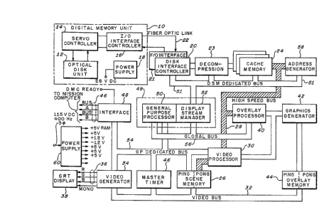
' A block diagram of t,he digital mapping system is
shown in Fig. 1. A mass memory unit 10 stores digital
image data representative of the area over which the
aircraft is to be flown and associated cultur ~ and
linear overlay features. The mass memory unit comprises
an optical disk unit 12, a servo controller 14, an
input/output (I/O) interfac,e controller 16 and a power
supply 18. Inormation stored in the optical disk unit
12 includes map information such as plan view
information from processed mapping data, plan view
information from processed paper maps, flight plan data,
terrain feature data and pictorial forma~. ~ mission com-
puter provides zoom, heading, scale factors, aircra~t infor-
mation and other parameters for modifying the ~o~mat of data
stored on disk. Data may be stored and recovered using any
of the well-known compression/decompression techniques.
Digit~ map data is stored in optical disk unit 12 1n
the form o~ sequential blocks or tiles. These tiles are
loaded as required into cache memory 24.
The present invention employs a cache memory in a
virtual memory address system~ In a virtual memory
system the disk memory is used as the main memory, so
that the operating program lS substantially independen~
of the actual amount of RAM in the system. The cache
_ . . . . . ... _ . .. . .
~3~6~5~
memory is used as a temporary memory for the map data
that is currently accessed by the process~r.
Periodically the disk memory is addressed and updated
information is loaded into cache memory. A virtual
memory system must provide hardware support for the
translation between the virtual (logical) addresses and
real (physical or absolute~ addresses. The virtual
memory address space is further divided into fixed
length units, which herein are defined to c~rrespond to
buffer segments in the cache memory.
The virtual memory system allows only those
sections of data currently being referenced to be stored
in RAM, with the rest of the data being stored on disk
or other mass memory. When new data is required, it is
brought into the cache memory and replaces the data no
longer required. It i8 a feature o~ the present
invention that segments of cache memory may be loaded
with data anywhere in the virtual memory address space
and logically addressed anywhere within the physical
address space. Methods ~or translating between virtual
addresses and physical addresses are well known.
Interface controller 20 controls mass memory disk
unit 12 for extra~ting the map data signals or overlay
data signals and periodically providing updat~d images.
On command o~ the disk interface controlIer 20 plan view
information i~ processed over fiber optic link 22 by
.. . . .
~3~ EiO59
--10-- ,
applying the stored map information to a decompression
circuit 23 that is compatible with the compression
algorithm, and reading ~he decompressed data into the
cache memory 24 which is also loaded with~encoded color
and intensity information. The cache memory is used to
buf~er the digital map data as it is retrievcd from tl~c
optical disk unit and to store the out-o~ view map
segments stored in look-ahead fashion ~or later view-
in~ and the segment descriptor tables. Thus the map
display can be built up without the inherent delay of
accessiny the optical disk unit, thereby allowing a
real-time display update rate. Data in the cache memory
24 will preferably be stored in north-up format centered
at the aircraEt location where ~he data was requested.
The data in cache memory 24 is then mapped to a scene
memory 26 via a high speed bus 28 and a video processor
30. The scene memory 26 is approximately one fourth the
size of the cache memory. Scene memory 26 is comprised
of a ping-pong memory so that one section can be updated
whlle a ~econd section is being read out. When the
scene memory is fully loaded, it is read out on video
bus 32 to video generator 34 which comprise~ the
waveform generation circuitry and a digital-to-analog
converter for decoding and conversion to an RGB or
monochrome composite video format. The analog signals
~5 on RGB lines 36 are coupled to a display 38 for
presentat~on to the pilot. Display 38 is typically of
.....
~1.3(~ )S9
the cathode ray tube type, although other types of
displays are also suitable.
Data continues to be processed from khe cache
memory as long as the information to fill the scene
memory is contained within the cache memory. When the
scene ~emory moves outside a predetermined buffer zone
within the cache memory, a ncw upda~c rrom ~ho op~ical
disk unit 12 is required.
Video processor 30 contains
color lookup tables, contour analysis, and bilineaar
interpolation circuitry. Contour lines are generated by
the video processor 30 and may be selected or deselected
as required. The contour line information is mapped
into scene memory 26 where it is also mixed with feature
data. Feature and other symbology is generated by the
overlay processor 40 which drives a vector generator 42
writing into a full field bit-mapped overlay memory 44.
Feature information i8 received from the optical disk
via the cache memory in an ASCII symbol and primitive
vector format. Symbol information may include a symbol
code, XY position within the map sector, and latitude
and longitude of the map sector. other features such as
roads, railroads, and rivers may be embedded in the
terrain data structure. The overlay processor 40 mav be
programmed to edit out symbols not in the field
represented by the overlay memory 44 and to rotate and
~;~06~
-12-
translate the display ~rom a north-up ormat to any
other desired direction and to write the complete
display into the overlay memory 44. The overlay memory
44 is also comprised of a ping~pong memory. The scene
and overlay memories are scanned in synchronism by a
master timer 46 via video bus 32 and decoded and
converted to RGB video in video generator 34.
A mission computer (not shown) resident on the
aircraft collects data ~rom various avionics subsystems
and generates - digital signals indicative of the
aircraft's present longitude and latitude coordinate
positions, a heading signal indicative of the angular
direction of motion, and signals corresponding to the
desired map data and overlay data. BUs 46 transfers the
command and status signals from the ~ission computer to
an interface I/O 48. Interface 48 couples the command
and control data ~rom the avionics mission computer to
the digital map display system. ~ control processor 49
includes a general purpose processor 50 and a display
stream manager 52. The general purpose processor 50 is
coupled via a dedicated bus 54 to inter~zce 48 and
controls data transfer with this mission computer.
Received data, data to be transmitted, storage buffer
addresses, and interrupt information are transferred
between the mission computer and the general purpose
processor 50 via the dedicated bus 54. By the use of
direct memory access a complete message may be rece~ved
.
_,~,, _ ~,, , _ , _, . " _ _ . . .. _ ._ _ ~
13~)60S9
and stored in the processor memory without loading the
processor itself. The general purpose processor 50
computes mode commands and status data from the bus; 46
information and transmitR it to the di~play ~tream
S manager 52. Display stream manager 52 controls display
operations and maintains a steady flow of data
throughout the system. It receives aircraft coordinates
and other parameters via the general purpose processor
on global bus 56 and uses this data to determine optimal
configuration of the system~ The display stream manager
will initialize the disk controller with data or command
func~ons and will have the disk interface steadily
streaming data which is soon to be required for display
into segments o~ the cache memory. Once all the data
13 necessary to build a display is resident in
the cache memory, the display stream manager 52
initializes the address generator 58 and the overla~
processor 40 to begin processing the scene memory and
graphical overlays. ~he address generator is
initialized with a base address, length, and orientation
parameters to extract display data from the cache
memory~ Cache memory 24 is organized as a virtual XY
Cartesian system. The display stream manager 52 can map
the memory segments in the physical address space
anywhere in the virtual system, which comprises the
entire optical disk memory, in~a manner to be described.
_ _ ...... .. . .... ..
...... _ _ _ .. . . . . .. .. _ _ _ _ . ... _ .... ..
~V~059
The overlay processor acts in parallel with the display
stream manager in building a display. Since separate
map terrain and graphic overlay memories are provided,
both displays can be built simultaneously. The overlay
processor combines all alphanumeric and graphic
symbology and terrain feature data into a separate
memory in real time. Prior to the address generator 58
extracting data from the cache memory 24, the overlay
processor 40 reads descriptor data from a segment
descriptor table in the cache memory. Once the overlay
processor 40 has extracted its descriptor table, it
begins to build a bit-mapped graphics overlay via
graphics generator 42 to the overlay memory 44.
Fig. 14 shows an overview of the top-level data
flow in the system of Fig. 1. ~ig. 15 shows the bus
interconnections between the general purpose processor
50, display stream manager 52, overlay processor 40, and
address generator 58. Appendix A is a description in
tex~ ~orm of the data flow between the various
processors. Figs. 16-29 relate to Appendix A and are
described therein~
RefPrring now to Fig. 2, the Cache Memo~y is a
group of 16 memory segments Ml M16, each logically
organized in a 256x255x8 bit array. The number of
storage segments provided is substantially less than the
number of segments necessary to store a complete map by
_ __......... .. : ... . .. __ . , . .. . . ... . .... . .... __
~11.3~ )59
virtue of the cache memory addressing scheme. Since a
typical scene requires 512x51~ pixels, and 8 bits for
the color descriptors, four seqments are re~uired to
make up a bit-mapped scenle in north-up mode. ~he
additional segments are required to a~sure that as the
display is rotated (for trackup displays) and translated
(for aircraft motion), there is sufficient memory
available to support the display. Thus, in Fig. 2~
segments N2, M3, M5, M6, M7, M8, M10, Mll, M14, and M15
are required for the rotated display7 Segments Ml, ~4t
M13, and M16 are unused. Each ~egme~t in the cache i8
individually controlled and can be allocated to the
display stream bus 51 for loading in data off the
optical disk 12, or to the high speed bus 28 for loading
the scene memories. When being loaded by the optical
disk, the memory is logically configured as 641C bytes
allow optimum data transfer from the disk with a minimum
o~ mapping~ When supporting the scene memories, the
memory is configured as a 2~6x256x8 image plane. Each
cache segment is logically configurable with re~pect to
its physical position within the overall image plane.
In operation, the aircraft's current position is
always taken to be the origin of the cache image planeO
Thus, as the aircraft ~lies towards one edge of the
display space, a cache segment that was behind the
aircraft may be updated with new data from the optical
.. . .
.. _ _ . . ... .. .. . . . . . .
.3~60S9
-16-
disk a~ logically replaced in front of the aircraft's
current position.
Fig. 3 shows the physical cache memory addressing
space and the arrangement of the cache memory buffer
segments therein. Thus, the address space is seen to be
configured in the form of an X, Y coordinate system with
an origin 0,0. The display system manager S2 has the
capability in the absolute cache memory addressing space
to address a total of 256 buffer segments. There are n
rows of buffer segments and m columns of buffer segments
which in a 256x256 word array encompass addresses 0,0
through F,0 along the X direction and 0,0 through O,F
along the Y direction. It is a feature of the present
invention that each of the buf~er segments xi,y; are
randomly programmable elements whi~h may be dynamically
relocated in the overall image plane to accomodate
changes in the aircraft's coordinate position. Since
each buffer segment is individually addressable, the
cache memory 24 is responsive to control signals from
display stream manager 52 to simultaneously read data
out of a first buffer segment portion and write new data
into a second buffer segment portion. It may be seen
from Fig. 3 that each buffer segment is independently
programm~ble with respect to its logical position within
the overall physical X, Y coordinate system addressi~g
space to form a predetermined image plane and thus that
.. . .
. .
:.......... :
. ~. ,
:. . ; .
. ,' . , .
...
.:
each buffer segment is addressable both by its absolute
position in the physical address space and by a logical
position within the virtual image plane. Each buffer
segment has 64K storage elements, wherein each storage
element can store therein at least one bit of map data
or overlay data and each storage element has a
corresponding logical address within the physical
address space. Preferrab:Ly, the cache memory buffer
segments will be configured in a plurality of parallel
image planes having corresponding storage elements in
each plane and wherein each corresponding storage
element in each plane has the same address for
collectively storing a digital word representative of
color and intensity of a displayed pixel. It is the
function of the display stream manager 52 to keep track
of the logical and physical positions of each buffer
segment and to program the cache memory in accordance
with the aircraft coordinate position.
Fig. 4 disclsses a block diagram of the cache
memory. It comprises essentially four major areas: the
input address selectors, the buffer segment and display
list memories, the input/output data buffers~ and the
buffer segment controller gate array. Fig. 4 shows
three buffer segments and supporting circuitry out of
the 18 segments utilized in the present invention. ~he
additional buffer segments and supporting circuitry are
: . :"
.. ..
': " ' ''"' ''~', . ' :'`
:,. "~.' ,' .. ' ~ '
13~60~i9
-18-
identical in structure and operation to that of Fig. 4.
The cache memory ~unctions as a dual-port memory
comprised of 18 segments, with each segment being
logically independent and under control of the display
stream manager 52. Digital data is transferred to the
buffer segments one segment at a time, and a segment of
data bits to update the scene or overlay memories is
sequentially scanned over a plurality of the segments
which are logically organized in accordance with the
physical address spacel but not necessarily contiguously
within the array of buffer segments. While one segment
or display list is being loaded with information off the
optical disk unit 12 through decompression 23, another
segment can be accessed by the address generator 58 for
transferring data to the video processor 30. Individual
segment control is proressed by the display stream
manager through the loading of dedicated mapping and
control registers located in the ~uf~er seg~ent
controller. The cache memory also contains 18 display
list buffers which hold the feature overlay information
associated with each of these 18 segments.
To accomodate an alternate display mode where
additional inormation is required, the segments may be
configured as a total of nine segments, each 16 bits
deep. ~hus, the cache memory physical address spac~ may
be configured either as a 256x256x8 or 256x256x16 image
.
. , , , ,~ :
,. ~
... . ............................ ..
.: , . ;
. ': ;' . .
.: . .. , ' :..
~3~ rJ9
--19--
plane.
The input address selectors provide for the
selectlve addre6sing of a bu~fer segment or display list
by the address generator, mass memory interface or
display stream manager under the control o~ the buffer
segment controller 72. The buffer segment controller 72
uses three control lines per segment to select which
function will address any given buffer segment or
display list. Address selectors 60, 62, and 64 are
selectively coupled to address generator 58 on line 66
for reading data corresponding to xi and yj locations in
cache memory. The xi and y~ addre~ses are read from a 24
bit address bus 66 of which 12 bits form each address of the
cache memory. Each 12 bit address is comprised of a 4 bit
segment tag and an 8 bit address in the bu~er segment or
display 11st. (See Fig. 3). The address ~elector~ are
also coupled to the decompression engine 23 via 16 bit
address bus 68 to address the tota~l buffer segment
address space of 64K words. A 16 bit address bus 70 is
also coupled from the display stream manager 52 to allow
the display stream manager to address the total buffer
segment addresis space of 64K words.
The bu~fer segment and display list memory is
organized as follows. Each buffer segment 80, 82, 84
consists of eight 64K 1 static rams organized as
256x256x8 bits deep. Ea~h buffer segment is associated
' '~.:. .'
. .;. .
., : "' , '
.. .s
.
~3~
-20-
with a corresponding display list memory 86~ 88, 90, in
which is stored feature overlay information and which is
2Kx8 in size. The address selectors 60, 62, 64 are
respectively coupled via a 16 bit bus 61, 63, 65 to a
corresponding display list memory and buffer segment
memory. Read/write and chip enable signals are issued
from the buf~er segment controller 72 via a 5 bit bus
67, 69, 71 to control access to the memories. Three
control lines are used to energize the display lists: a
read/weite line, an output enable line, and a chip
select line that places the memory in low-power standby
when not being addressed. Each buffer segment has two
control lines: a read~write line and a chip select line
that places the bu~fer segment memory in low power
s~andby when not being addressed. Buf~er segment memory
80 is coupled via an 8 bit bus 92 to an output buffer
94. Output buf~ers 96 and 98 are correspondingly
coupled to their respective buffer segment memories.
Output bu~fers 94, 96, and 98 are coupled in common via
a 16 bit bus 106 directly to the video processor 30 to
provide display lists or buffer segment data during
address generator read operations. Buffer 100 receives
buffer segment and display list data via bus 108 for
energizing the overlay processor 40. B~ffers 102 and
2~ 104 similiarly receive data from their associated
memories for coupling to the overlay processor. Buffers
,
".: ' ,' ',
, . . ..
:
,. .
..
: ,:
'''' ' ' `
21 72519-l9
lO0, 102, and 104 also accept data from the decompression
circuit 23 to be written into selected buffer segments and
display lists. By using combinations of control signals
available from the buffer segment controller the input/output
data buffers are selectively enabled.
Fig. 5 shows a block diagram of the video processor
circuit. The video processor takes video data from the cache
memory, x,y coordinate addresses from the address generator,
address and data signals from the overlay processor, and
control signals from the general processor to produce an 8 bit
color word to be writ-ten into the scene memory. The video
processor processes linear feature data to determine if a
linear feature is to be written in a given location. It also
determines the color of a location based on the elevation of
the terrain. The color of a specific elevation is programmable
by the general purpose processor through the use of lookup
tables to be described. When the color value at a desired
location falls on a non-integer location, a bilinear
interpolation is performed between four neighboring points
provided by the address generator to determine the actual color
value at the location to be written. A suitable circuit for
bilinear interpolation is shown in the W. W. Knight U.S. Patent
No. 4,402,012, Two-Dimensional Digital Linear Interpolation
System, issued August 30, 1983 and assigned to General Electric
Co .
~ s~
:~3~ S9
22 72519-19
The video processor is also used to determine when a contour
line is to be written. Contour lines are used to delineate
changes in elevation in the manner described in Canadian patent
application No. 567,610, Digital Contour Line Generator, filed
May 28, 1988. The color of a contour line is programmable by
the general purpose processor. Linear features and contour
lines may be selectively enabled so as to assign a priority to
a desired form of display. The video processor also produces
sun shading as a function of reflectivity maps representative
of the sun azimuth in elevation and the aircraft heading. A
further feature permits displaying dynamic color zones
representative of ranges of elevation, either in absolute terms
with respect to the terrain elevation, or relative to the
aircraft altitude. The signals from the color band generator
and the sun angle intensity may be combined to derive a
composite signal in red/ green, blue primary color format. Map
data may also be passed directly to the scene memory where it
is not desired to display the color features described above,
or this map data may be disabled giving the linear data
priority over the map data at that location.
As shown in Fig. 5, the operation of the video
processor is controlled by the general purpose processor via
address and data signals applied to decode and control latch
120. The control status will strobe the
~l3~6~9
-23-
control latch in a conventional manner~ The video
processor includes a linear feature generator comprised
line~ feature
of an address encoder switch 122, a~ode book 124, a
select/de~elect ~witch 126, and a color lookup table
128. The lookup table provides a powerful mechanism for
rapidly changing the definition of display pixel values
without changing any display data. For this purpose,
lookup tab~e 128 is coupled to the general purpose
processor which provides programming of the desired
color table ~n a conventional manner. The encoder
switch 122 receives address slgnals ~rom the overlay
processor for selecting one of nine segments from code
book 124 and segment enable command signals from the
cache memory. It is also coupled to the high speed data
bus 130 for receiving linear feature overlay commands
which will ~elect one of a plurali~y of linear feature
combinations stored within code book 124. Code book 124
is programmed by data from the overlay processor and
typically stores up to 30 possible linear features.
Each linear feature within the set can be enabled or
disabled to form any combination of linear features to
occur a~ any elevation point. The linear features~may
al~o be arranged in order of priority. The code book is
compri~ed of a random access memory programmable by the
overl ~ processor. When the address generator loads new
segments of data from the optical disk to the cache
:. .: .,
. . .
'". ':-"
.
.: .. :"
;,
.,, ! ~
1 3060S9
-24-
memory, it will also send a display list describing the
combination of linear features in each segment to the
overlay processor. The overlay processor will then
update the code book based on the display list it
receives from the address generator. The outputs of
code book 124 are coupled to switch 126. Switch 126 may
be comprised of a mask which is enabled by the general
purpose processor. Each linear feature thèn can be
masked out independently of other linear features. If
desired, the output from switch 126 may be applied to a
priority encoder (not shown) whereby when a linear
feature is masked out the linear feature with the next
highest priority will be displayed if it is not masked
out and is ena~led. Thus, when a contour line appears
at the same elevation point as a linear feature, the one
with the highest priority will be displayed. The switch
outputs or priority encoder outputs are then applied to
a linear feature color loo~up table 128. Table 128
produces the color of the individual linear features in
a red, green, blue primary color form. Typically, a 5
bit code ic used, providing 32 color values.
Dynamic sun angle shading is used to control the
intensity of the colors, thus simulating shading of thé
terrain. A plurality of reflectivity maps are stored in
lookup table 132. The general purpose processor
provides a map select signal for selecting one of ~he
.;
.,., . ,j .
., ~ .. . .
'~, .', .. .
:. :. .
~3~6~)59
-25-
previously stored maps. The processor may also load the
lookup table wi~h the desired reflectivity maps. Based
on the sun azlmuth, 6un zenith, and aircraft heading,
the general purpose processor selects one of the
prestored reflectivity map,s. Selected surface normal
lines derived from the data bus are then applied to map
132 to select one of 32 intensities within the map. The
output of the map is in a ~Eorm of a 5 bit binary code
describing the intensity.
Elevation color bands are provided by lookup table
134. This circuit utilizes the elevation data at each
pixel location to perform a table lookup on hue.
Aircraft altitude may also be con~idered to obtain an
offset into the table so that the hue tracks over the
terrain relative to the aircraft altitude. Thus, the
hue may be defined either in terms of absolute altitude
of the terrain or relative altitude of the aircraft with
respect to the terrain. For programming the lookup
table 134, it is coupled to the general purpose
proce~sor. Color bands define zones of a predetermined
range of elevation. The elevation at each displayable
pixel is applied as an address to the color band lookup
table 134. Typically, table 134 is ccmprised of a 256x4
RAM. In relative mode, the lookup table is updated at
the border~ as the aircraft changes altitude.
The outputs from lookup table 134 and reflectivity
.,.'. .. ~,''~ . ~ " '. ''
:. ,,. ~ .
"''," "',' ~ :
'' ~'', '.'.,, ' ',~ '' ,''.
; . .~;'~ . :
~ ~)6 [)5~
-26-
map 132 are applied to a further lookup table 136.
Table 136 combines the intensity and hue to provide a 5
bit output for the red, green, and blue primary colors
with a range of 32 intensities for each color. The
three primary outputs are then applied to corresponding
bilinear interpolation circuits 138, for an
interpolation in each colorO
A further feature is provided by contour analysis
circuit 140. The contour line circuitry uses an edge
detecter and averages the elevation data for comparison
with one of a plurality of lookup tables with
predetermined contour line spacing. The contour line at
a selected pixel location may be suppressed or may
overwrite the pixel to allow for instant select/deselect
on c~tour lines, by means of circuit 142. Circuit 142
is comprised of a conventional enable/inhibit register.
The output of register 142 is'applied to a color encoder
lookup table 144 which reduces the 15 line data input to
an 8 line data output, which is then applied to the
scene memory. When desired, the linear features,
reflectivity map, color banding, and contour analysis
may be deselected and video data applied directly to the
scene memory through buffer 146.
Referring now to Fig. 6, a scene memory apparatus
implemented in accordance with the present invention s
illustrated. The apparatus includes a pair of
.. ;
.
.' :' , ',:
~30~(~S9
-27-
full-field refresh memories 150 and 152. Each of the
memories 150 and 152 comprise, ~or example, 512x512x8
bit static RAM memories, where each address represents a
pixel on the video display. Input data to be written
into each of the memories 150 and 152 are provided on
busses 154 and 156 respectively. Memory 150 is
addses~ed by bu3 158 and receive~ a write command on
line 160. Memory 152 is addressed by bus 162 and
receives a write command on lead 164. In the embodiment
of the invention illustrated in the figure, 484x484
pixels and 242x242 pixel display modes are s~pported. A
ping-pong control signal 163,165 from control register
166 is used to ~ssign a memory to the address bus 168a
or 168b and the video processor data bus 170 while the
other memory is assigned to the video generator address
bus 172a or 172b. Ping-pong operation is effected
between the full field memories 150 and 152 by
sequentially reading in data to one memory while reading
out the stored data in the second memory and then
updating the second memory with new frame data while
reading out the first memory. Addresses for writing
data into ping address multiplexer 174 and pong
multiplexer 176 are provided on busses 168a and 172al
and 168b and 172b, respectively. Control register 166
~5 receives commands from the control processor including
read and write signals, block select, address select,
'' ', .~; : :
.: ., ~: .,:
., . , j., .
',:
' ^':' '.~' :
... .. .. .
~3~6~
-28-
and a clock signal. A ping-pong select signal which
causes the memories to alternately and sequentially read
in, store and read out data is provided by the timing
generator. A strobe pulse for reading in video
processor data is provided by the address generator9
The output of ping memory 150 is coupled on a bus 178 to
a multiplexer 1807 The output of pong memory 152 is
coupled on bus 182 to multiplexer 180. The outputs on
busses 17~ or 182 are selectively controlled by a signal
from control register 166 on bus 184. Multlplexer 180
provides output data from memory 150 or memory 152 to
the video generator on bu~ 186
In operation, the PI/PO select line 188 is applied
to control register 166 to determine whether the address
generator or the master timer, which generates the video
generator address, will address the memory. Thus, if
the PI/PO select line is high, the address generator has
control of the ping address bus 168a or 168b, while the
master timer has control o~ the pong address bus 172a or
~0 172b. During this time, video processor data is wri~ten
from bus 170 into the ping memory 150 while data is read
from the pong memory 152 into MUX 180 and to the video
generator. When the PI/PO select line goes low, the
control register 166 switches memories and the address
~5 generator then has control of the pong address bus while
the master timer has control of the ping address bus~
",,,."", iis~ '
. :,. . . .
..
:. , ",
' ,.: :, '......... .. .
:.: ... : j , . :
~3~60~9
-29-
In the present invention, each o~ the memories lS0
and 152 is organized into four banks o 512x128x8
memory.
The sequential operation is controlled by the
control register 166 which can be read or written into
by the control processor.
E~ept for the number of bit planes, the scene
memory 26 and overlay memory 44 are identical in
architecture. ~hile the scene memory implements two
double-buffered 8-bit display planes, the overlay memory
utili2es two sets of 4-bit memory planes, one for each
set of scene memory planes. Each overlay memory array
is S12 x 512 x 4 with an effective viewable display of
484 x 484 pixels. Each overlay memory is capable of
being assigned to the overlay processor 40 ~or update
or to the digital video bus 32 for re~reshing the CRT
display.
Graphical data ~rom the graphics generator 42 can
be written into any combination of memory planes within
the overlay memory 44. This allows planes to be
assigned to different predetermined types of symbology
which can be enabled or disabled by setting a control
bit~ Thed~is~lay stream manager 52 controls the bit
'' . .: ~. ' ' ` .'
.:
,." ~"'"''
.. ... ...
~3~6059
-30-
plane options and communicates that status to the
overlay processor.
Display refresh is controlled b~ the mas~er timer
46, which synchronizes scene memory readout with the
overlay memory readout to support the display refresh
requirements. Four adjacent pixel locations may be read
simultaneously and loaded into shift registers, which
are then clocked at the video pixel rate for reading out
the stored data. A ping/pong line from the master timer
46 controls which set o~ memory is accessed by the video
generator 34 or the graphics generator 42.
The overlay memory 44 interface~ with the video
generator 34 via 4 data lines. The ma~ter timer 46
feeds 18 address lines and a ping/pony lineO The
interface with the graphics generator 42 is via 4 data
lines, 18 address lines, a read jwrite liner a control
strobe line, a reset line, and a data valid line.
The circuit o Fig. 7 shows the interconnection o~
an address generator 192 to the map display system.
~ddress generator 192 is coup}ed via address
and data bus 200 to control proce~sor 190. The bus 200
also provides address and data signals and receives
status information from cache memory 194, video
processor 196, and scene memory lg8. Address generator
192 provides read address commands along the x and y
coordinates via bus 201 to cache memory 194. The data
~ .
.' ' ~ ,
.. ' . ,' ,~, '
. . .~' "
: - ,,'c
~l3[)EiO~
-31-
read out of cache memory 194 is coupled into video
processor 196 and overlay processor 208 via data bus
203. Address generator 192 also provides a read address
via bus 201 to video processor 196. When video
processor 196 has completed its operations on the data
received from cache memory 194, it provides the
processed data via bus 204 to scene memory 198. Scene
memory 198 receives a write address via bus 205 from
address generator 192 and provides the data from video
processor 196 on an output bus 209 at addre~ses
determined by a read signal from video generator 34 on
address bus 210. A read control signal is provided on
line 207 by address generator 192 and a write signal via
line 206 to scene memory 198.
R~ferring now to Fig. 8, the structural details of
the address generator 192 a~e shown in greater detail.
Address signals from display stream manager 52 are
applied to a decoder 210 via a bus 212. Decoder 210
provides output commands such as initialization of the
initial x and y coordinate starting points, aircraft
heading, zoom ratio, and initial x and y line count.
The address generator consists essentially of four
function blocks: a read address generator 212, a write
address generator 214, x and y line counters 216 and a
state sequencer 218. Coordinate translation
coefficients to provide an upper left justified
.. '.' ' ~ ~
,. ,.:, ~ '':' '',''''
''' ' ' ;~, ,' '
' . ': :. ~: :
~3~0S~
-32-
coordinate system within the absolute cache address
space and rotation coef~icients corre&ponding to the
alrcrat heading are provided by circuit 220. These
functions may a1BO be provided ~y the general purpose
processor if desired. The commands from decode.r 210 are
coupled to read address generator 212 and write address
generator 214 on bus 216. Further commands to state
sequencer 218 are applied on line 22~. Line counter 216
receives its initialization commands on bus 224.
Functional block 220, which may comprise sine and cosine
memories to scale the sine and cosine values provides
the computed address parameters to read address
generator 212 and write address generator 214 on bus
226. Control siqnals from state se~uencer 218 are
applied to read address generator 212 via bus 228 and to
write address generator 214 via bus 230. Line counter
216 is coupled to controller 218 via bus~es 232 and 234
Controller 218 also provides read and write clocks and
control signals to tbe scene memory, video processorr
and overlay processor. The output of read address
generator 212 is applied to the cache memory 194 and
video process~ 196 via bus 201. Write address
qenerator 2t4 provides a write address via bus 205 to
scene memory 198 and overlay processor 208. The control
processor provides data signals via bus 236 to counter
21t, state sequencer 21~, function block 220, read
. "
'
:: ;
- ~1 3~6~59
-33-
address generator 212, and write address generator 214.
operation of the address generator ma~ be more
clearly understood by reference to Fig. 9
~ ~ , with continued reference to ~ig. 8. At the
start of each update cycle, the address generator, which
receives its control parameters from the display stream
manager through the decoder 210, is commanded to ~erform
a display list scan. Typically, nine consecutive 910
byte display lists filling a maximum of 8192 bytes will
be transferred to the overlay processor in this mode.
The lists are transferred consecutively and hence
written in consecutive locations in the overlay
processor. ~ starting address provided by the display
stream manager provides a segment tag to the overlay
processor which will identify the di~play list to be
transferred with its associated buffer segment. After
the segment tag has been given to the overlay processor,
the address generator then generates the read and write
addresses ts transfer the display list information from
the cache memory to the overlay memory 44. The read
address generators 212 are basically arithmetic logic
units which perform a seri~S o~ incremental adds after
receivin~ a starting point, pixcl-to~pix~l incremen
values, and line-to-line increment ~alues from the
function block 220. The initial x and y starting points
are calculated by the display stream manager using a
.. .. : ;:
. . ~ , .. .
.,,;, ,,~; .
.',''1 , '.;'
.'!
:, . ' ;,
3 ~ 6~ 5
-34-
normalized coordinate system and the aircraft heading
information~ These initial values are then loaded into
the respective x and y add~ess generation circuits.
Aircraft heading and zoom :information is also provided
to the address generator through data bus 236. Function
block 220 comprises addressable sine/cosine prom's which
determine the direction frvm the starting point and the
increment for each repetitive add operation. The zoom
information scales the sine/cosine values. The display
stream manager also provides the x and y translation
coefficients on bus 236. These coefficients are added
to the generated addresses to provide an upper left
justified coordinate system within the absolute cache
address space. The initial x and y line counts are
provided on bus 236 to function block 220, where they
are processed and applied to read address generators
212. In the display list mode, typically the x count
would be comprised of 256 pixels and the y count would
be comprised o~ 3~lines. In the map display moder the x
count is typically 484 pixels and the y count also 484
pixels. The count is adjusted to allow for the display
mode, such as bilinear interpolation, and high
resolution or low resolution operational modes. The x
and y initial addresses are also loaded into write
address generators 214. The write address generator~
consist of counters used to provide addresses to the
; :
.. : . s,,.' ..
''.' .". ~; ' .:
.'' .' ~ "
,, '', ,"",' ,;~ .' :.
:,. .. . .
61D5~
-35-
scene memory 26 for the transfer of display data or to
the overlay memory 44 for the transfer of overlay data.
They are clocked directly by the state sequencer 218.
As noted above, the x line counters are decremented
after each address pair is generated along the scan
line, while the y line counters are decremented after
the completion of one entire scan line. The outputs of
the x and y counters provicle a signal indicating when a
block transfer operation is complete. In the map mode,
the counters are loaded to take into consideration the
additional steps needed to find the four points used for
bilinear interpolation.
The state sequencer provides the address generator
with all of the necessary control signals and clocks
required for its operation during the different modesO
After the display stream manager has supplied the
addres~ generator with the necessary initialization and
; control parameters, it starts the sequencer. The
sec~uencer then provides the required internal control
signals based upon its multiplexed inputs to generate
the addresses and output control signals as necessary
~or the mode that the display stream manager ha~ loaded
into the address generator decoder. The state ~equencer
provides control signals to the video processor for use
in it~ bilinear interpolation circuitry, clock signa;s
to the cache and scene memories to read or write data,
, .
~3~ 5~ 725l9-lg
-36-
control ~lgnal~ to the overlay processor to tran~er
display lists, and clock signals to the video processor
and to the overlay processor. The multiple input~
include X done, Y done, bilinear done, last line,
address generator done, and other related ~iynals.
Referring now to Fig. 9 , after initialization
(300)~ the address generator reads an initial x, y
segment tag ~304~ into the cache memory. It then
asserts a write address (306) to the overlay processor
and provides a strobe signal 1308~ identifying the
segment tag to the overlay proce~sor. The x, y count is
stored in a latch ~310) and the x count decremented by
one (312). The x write addres~ is ~hen incre~ented
(314) and a write addre~s addressed to the overlay
processor (316). ~he corresponding read address is then
applied to the cache memory to extract the list data
stored therein (3183. The list data is then strobed and
applled to the overlay processor (320). The x count i8
then tested (3~2) against the predetermined number of
pixels in a line. If the x count does not correspond
thereto, the read address is again incremented ~324) and
the cycle is repeated. When the x count is completed,
this denotes that a complete line ha~ been scanned and
the y count ~8 decremented as ~hown in Fig. 9 (326~.
The x register l~ then cleared to set it up for a new
count (328). The y count is then tested (330) and if it
' :' ' ,.
- :. :
,
: :,
72519 l9
)59
-37-
has not been completed, the y read address is
incremented and a new address latched into the read
generator (332). The cycle ~hen continues, as shohn in
Fig. 9 until both x and y counts have been sa~lsfied
(334).
After the address generator has transferred all the
necessary display list information to the overlay
processor, it will be commanded to transfer the terrain
or map data contained in the traversed bu~fer segments
to the sc~e memory, through the video procassor, in a
similar manner. Map data will be operated on by the
video processor to obtain the data written into the
scene memory. In the map mode, the fractional x and y
address bits generated by the display ~tream manager are
passed to the video processor to be used in the bilinear
interpolation circuitry.
Referring to Fig. lO, a simpli~ied functional block
diagram o~ a graphics generator 42 is illustrated by
which simultaneou display of graphical images in vector
and raster form can be di~played along with map data.
The graphics generator 4~ includes an X deflection
accumulator 402 and a Y deflection accumulator 404 which
respond to de~lection ~ignals corresponding to
deviations from the origin along the X and Y coordinate
axes, respectively, ~or providing a substantially linear
digital output representative of a desired graphical
,
, ';........ , '.:
,:s
.. ..
4,
.~''~ ' ;
s~ ~
--38--
symbol to be superimposed on the dis~lay. A suitable
de~lection accumulator is shown in U.S. Patent No.
4,481,605, Display Vector Generator utilizing
Sine/Cosine Accumulation, ~iled March 5, 1982, and
assigned to the assignee of the prese~t invention. The
deflection accumulators 402, and 404 are controlled by
the output of a microprocessor 406 so as to deliver
signals corresponding to the various symbols and
features to be displayed during ~light. Data relating
to the identification of the various symbols and
characters are stored in a digital memory 408, which is
loaded by I/O control 410. I/O con~rol 410 receives
data and addres~ signals from the overlay processor 40,
and a 15 MHZ clock signal from the master timer 46. A
memory arbitrator 412 permits sequential access to the
memory 408 by the I/O control 410 and the processor 406.
A microprocessor 418 is coupled to mapping PROM 414
which comprises a look-up table o~ starting addresses in
control store 416 for each of the~microcode routines
that execute a graphics command. These starting
addresses are fed to the sequencer 418 in synchronism
with the sequencer being commanded by the microcode to
jump to the address at the sequencer input 420.
Procesfior 406 i~ controlled by routines stored in
control store 416, and the execut on of the routines ~re
con~rolled by the ~eguencer 418.
.
'. .,.. ' . ~ ,: `
:... . ~;
. . .
:: .
~3~:)6~59
The outputs of processor 406 are in the form of
primitive commands such as polar vector, tangent vector
rectangular vector, and rotate. During the execution of
tangent and polar vectors, incremented displacements of
S a displayed pixel are derived from a trigonometric
look-up table 422. During slews and rectangular
vectors, the data is derived from the processor 406.
These values are coupled to the inputs of deflection
accumulators 402 and 404.
The video control 424 is loaded with control data
specifying the type of graphics operation to be
performed with the corresponding data values loaded into
deflection accumulators 402 and 404. Color values are
determined by a look-up table within video control 424
to specify color and level of in~ensityt or the video
may be blanked on predetermined vectors.
In operation, the primary function o~ the graphics
generator 42 is to generate the color raster symbology
and terrain features that are to be ~uperimposed on the
map display. The~ type of symbology and its location on
the map are loaded into the memory 408 by the overlay
processor 40 on address bus 426 and data bus 428 via a~
fixed set of intermed1ate graphics instructions. These~
instructions are then processed to generate the overlay
information in the overlay memory 44 using vector
graphics techniques to generate polnts, lines, and
::
. '!
', ' ' ,!'. ' '
',~ '. ' ' . ' , ' ~.' "
': ';1 ``
.. ' . ;'
"' ' " ~ '
' ,j,.
,
~3~ 5g
--~o--
characters.
The gr~hics generator 42 may be considered as
comprised of two subsystems: an instruction processor
and a vector generator. The basic graphic element
produced by the vector generator is a straight line of
pixels. This line may be translated, rotated, and
concatenated. Vectors of various lengths and angles can
be combined to produce the desired overlay symbology.
The graphics instructions are received by I/O
control 410 from the overlay processor 40 and stored in
digital memory 408. A font character definition code is
downloaded into the memory and define~ the alphanumeric
characters and terrain features. Each font symbol is a
graphics routine comprised of either polar vector or
tangent vector commands~ An operational program is also
loaded into memory which controls the generation of the
desired overlay symbology. This program is updated for
each display frame. An additional memory area is
; reserved for command processing.
After a start signal is received initiating a new
cycle of operation, video control 424 is loaded with a
desired mode of operation. Processor 418 then writes
primitive vector instructions into processor 406 for
; transferring data into the X and Y deflection
accumulators. The accumulators then write the desired
vector pattern into the overlay memory 44 in incremental
.. ', '','., ~ , .
~, ~
.: , :- ~,~'.
ih
,~.
(16~9
X and Y data bits. ~ plurality of data words may be
stored in the accumulators and video control for
~equential execution. ~he color look-up table in video
control 424 is programmed by the overlay processor 40.
The graphics generator uses a standard Cartesian
coordinate system with horiontal X and vertical Y axes
as the reference for positioning symbology on the map
display. A graphics command is implemented that enables
the specification o~ the coordinate origin anywhere
within the image memory plane.
An overlay memory read strobe 430 is generated by
I/O control 410 when data needs to be ~ransferred from
the overlay memory to the instruction proce~sor. An
overlay memory write ~trobe is generated by the video
lS control 424 when data is to be transferred from the
vector generator ~o the overlay memor~
The particulax memory bankwritten to or read from
is designated by PI/PO selec line origina~ing in the
master timer 46.
The video generator provides the conversion of
digital display data from the display memories and video
synchronization signal~; rom tbe master timer into
RS-I70A type analog ~ignals.
A block diagram o~ video generator 34 is shown in
Fig. 11. Scene memory data (8 bits) and overlay memory
data (4 bits~ and the pixel clock are latched into
'
. . .
"
,
~l3~60~9
-42-
latches 450 and 452, respectively. The pixel clock is
at the predetermined pixel rate. The scene memory is
operative in either 282 or 484 line modes. The 242 line
mode is synchronized in such a way as to latch in data
from the scene memory when the data from the overlay
n~emory i8 latched at an even addr~s, while both
memories are read contiguous:Ly. In this manner, scene
memory data i8 latched in every other addr~O Al].
timing i~ digitally gener~ted by the master timer 46.
This includes pixel clock, horizontal sweep signals, and
a composite sync signal.
The output of scene memory latch 450 is applied on
an 8 bit bus 454 to color conversion PROM's 456, 458~
469, and 462. The PROM's are 8 bit color or monochrome
look-up-tables in which are encoded a predetermined
range of color values and intensity, so as to provide
the primary red, blue and green components or a
monochrome output in digital format. The color and
monochrome data conversion is implemented in 16k x 8
RAM's and loaded by the processor 50 on power up~through
a 16 bit address line 464, 16 bit data line 466 and data
bus interface 468. A memory write signal on bus 470
allows the RA~ look-up tables to be loaded via bus 472.
Each RAM i 8 bit~ wide, RO that the proce or loads two
colors simultaneously. The red and blue are loaded at
one time, as are the green and monochrome. This enables
: . , . . - .
. . . . . .. ... .
:. . ~
. .- . ' . .
', . . :'.' ' : ';
. , ;. . :
~ ~16~9
-43-
loading of the look-up tables to take place twice as
fast as if each color were loaded separately. A map
enable signal is fed through latch 452 to the look~up
tables 456, 458, 460, and 462. This signal is used to
allow data from the overlay memory to be displayed while
inhibiting the display of data from the scene memory.
The output from each of thle red, blue~ green and
monochrome RAM's is fed on respective 8 bit buses to
corresponding digital to analog convertors. The DAC's
474, 476, 478, and 480 convert the digital inputs to
analog outputs. Pixel clock 1 is also applied to the
DAC's on a bus 482.
When the monochrome mode is selected, DAC 474 and
476 are disabled by a blank 1 signal~ The blank 1
signal ls applied when the video is to be blanked for
the red and blue outputs for vertical and horizontal
sync, video disable, monochrome mode, and line video
sweep. The ~lank 2 signal is applied only to DAC 470
and 480, but the monochrome mode has no impact on this
signal. The red and blue DAC's use a different blanking
signal than the green and monochrome DAC's due to the
fact that red and blue must always be blanked while in
the monochrome mode. The monochrom~ signal is applied
to green DAC 478 through a MUX 484 coupled in series
with green look-up table 460. A sync signal is applied
only to the green and monochrome DAC's~
?',
, ?
. . ' . ,.' .:
:. ; :
.... :- :
:: . . , ,; .
,.......... : ~ .,:
: .~ ::.
:. ,:.
~3 [)~ 9
-44-
The analog color outputs are each fed to a buffer~
The buffers 486, 488, 490, and 492 are coupled to
corresponding inputs 36 of the CRT display 38.
CRT 38 may be comprised of a multicolor cathode ray
table. Each buffer is connected to drive a red, green,
or blue gun or to provide a monochrome signal.
Disk interface controller 20 serves as a mass data
controller for loading map data siynals and overlay data
signals from mass memory unit 10 into the cache memory
24. It is comprised of a fiber optic interface 21 and a
di~k controller 20. The fiber optic interface 21 is
comprised of optical to electrical conYersion circuitry
and electrical to optical conversion circuitry, a
parallel to serial data convertor, and a controller.
The disk interface controller 20 is comprised of a
timing generator and disk read/write storage command
memory, and converts the received serial signals to
parallel form.
In operation, the disk controller 20 receives
instructions from display stream manager 52 via the bus
51. These instructions initiate block data transfers to
and rom the digital memory unit 10~ The instructions
define the location of the required data on optical disk
12 and the number of data blocks needed. When the data
transfer is complete, controller 20 signals display~
stream manager 52 and awaits further instructions. The
:.......... ,., .:- .
'.'. . : .' ' ' ' . '
'; '.
'', : '
::.
~IL3~6 [)59
-45-
timing generator controls the bus ~, which is a
synchronous, time division multiplexed bus.
The fiber optic conversion circuits convert optical
signals to TTL digital signals, and vice versa.
Master timer ~6 provides a common timebase for the
generation of all timing signals to produce the
composite video signal. Master timer 46 generates clock
signals at the pixel rate of 9.26 M~z. It also provides
horizontal and vertical blanking, horizontal and
vertical sync, and generates sequential addresses for
the purpose of synchronizing the scanning of information
stored in the scene and overlay memories for developing
pixel data. Horizontal and vertical sweep signals are
generated to define the active window of line video
display.
Timer 46 supports two display mode~: 525 lines at
60 Hz rate and 625 lines at 50 Hz rate, both supporting
2:1 interface. Preferably, t~here are 484 dispIayable
pixels per line, but scene memory data may also be read
o~t at a rate of 242 pixels per line while being
displayed at 484 pixels per line b~ reading each pixel
twice.
Horizontal and vertical blanking and
synchronization pulses are generated in accordance with
EIA RS-170A Standard, which i5 well known in the ar and
is hereby incorporated by reference~ Preferably, all
. ' . ......................... ' .:
.,,' ' ,.'. ~ ..
.; . .~ .:
~, ,
59
-~6-
signals are generated from a common timebase to maintain
absolute relative relationships.
Referring now to Fig~ ]L2t wherein the timing
waveforms shown are not drawn to scale in order to more
clearly show the structure, in operation a train of
pixel pulses 502 is generated at 90~6 MHz, which results
in a pul~e duration of 108 ms. A horizontal scan signal
establishes the rate between BUCCe8SiVe lines of the
display, and is typically of the order of 15,750 Hz for
a 525 line display. This results in a time interval 504
between the end of one raster line and the end of the
next, including retrace o~ 63.5 us.
The two memo~ies are addressed in a synchronism
with the pixel clock pulses, as shown at waveform 506
The horizontal scan is blanked during retrace by a
blanking pulse 508. A horizontal sync pulse 51~ is
generated during the blanking interval for synchronizing
th~ hori~ontal scanning circuits in a conventional
manner. The horlzontal l~ne video si~nals are a
varlable, depending on the width of the window to be
displayed, hence are not shown. The vertical ~ignal~
are generated in a similar manner at a 60 Hz or S0 Hz
f rame rate.
Figure 13 shows corresponding vertical blanking and
sync signals for a 20 ~z frame rate for loading and
reading the scene and overlay memories wherein each
; :,' '.
. '. ' ............................................. .
.;~.
,. . :: ,~
~3~6~
frame is 50 ms in duration. Each field is 16.67 ms in
duration, and three fields are generated for each frame.
The ping-pong select signal PI/PO alternates between a
logic high and logic low for each successive frame.
When PI is high, the timer addresses and writes pixel
data into the PI memories, and reads out data previously
stored in the PO memories When PO is low, the timer
reads out the data stored in PI memories, and overwrites
new pixel data into the Po memories.
While the invention has been described in its
preferred embodiments it is to be understood that the
words which have been used are words of description
rather than limitation and that changes may be made
within the perview of the appended claims without
departing from the true scope and spirit of the
invention in its broadest aspects.
','... '.
:: . .: .: . .
:. .:........ , ;. :
.,: , i . :
3 3~iO59
- APP13NDIX A -- PROCE~SSOR FUNC:['ION SUMMARY
A~ 3~059
GPP FUNCI'lON SUMMARY
- RESPOND TO 1553 RECV,XMIT MESS~GES FROM THE MC
INTER-PROCESSOR COMMUNICATl~N BETWEEN GPP '> OLP
GPP -> DSM
- UPDATE: Il/W DEVICES FOR COMM-~NDED DISPLAY MODE
- Vl DEO PROCESSOR
- Vl DEO GENERATOR
- MP~Sl'ER 1'1 MER
- 1553 lN'I'ERFl~CE
... . ,, _ . .. , .. _ _, . ..
RECV/VALID WORDS
These words are in the last block of ~ECV RAM
Bit positions in these two words correspond
to which word in the Command Word Section
the correspol)ding 1553 message comman(l
wotd ran be fo~ l, and whjcli l)llfrer cntry in the
RECV Message Section the message can be ~oun~
(e.g.) bit 2 implies ~hat the second word ir-
the Command Word Section contains ~ttle command
word for the RECV message Lhat resides in the
second message buffer of tlle RECV Message Section
Bit 0 of the first wold D~ it l5 o~ t~le sceorld word
are always set to zero since tl~ey don't. point to any
valid RECV message bloch in the RECV Message Section
_ ~,_ _ _ , . ~ . ....... . _ _~__ _ .,. . ._.. :.... _ ~ . . ., ___~
os~
~-2
~ 1553 IIECV II~M
lK 1553 RECV RAM partioned:
- RECV Command Word Section (32 wrds)
- RECV Message Section (30 32 wld msg hlocks)
- RECV/VALID and Spa~e Section ~32 wrds)
~he RECV Message Section consists of 30 message
blocks in which 32 data words cao ~)e stored
.
- Messages are placed in RECV message section in
the order they are received ftom tlle MC
As the next RECV message arrives:
: - the 1553 command word is placed at the ncxt
word o the Command block in RECV R~M
- the next bit position in the RECV/VALID word
is set to indicate a valid message received
tl)~ message dat~ is p]aced at the next availa~le
messa~e, b~ock in tlle Qlleue
(SEE FIG. 16)
FIG. 17 FOLLOWS
:;
~3~6~59
A-3
.......
GPP proces5in(J oC QECV Mcssage lnterrupts
GPP inspects RECV~v~LlD word for:
location in Command word Section for msg command word
- location in RECV Message Section lo~ corresponding
RECV ' ed mes sa ge
GPP moves message from REC-v RAM to ei ther Inter-Processor
Shared RAM or a GPP holding queue
When the GPP finishes processing a RECV message,
the GPP checks for the arrival of more messages
that were received du~ing the time the Grp was
processing the previous 1553 RECV message.
GPP has capability to select any one or all messages
to generate a 1553 RECV interrupt
_ . _ _ . . .. . . . . . .
~L30~;0~i9
A-4
~ 1553 XMIT R~M
IK 1553 XMIT RAM partioned:
XMIT Lockout lndicat~l Section (32 wl~ls
XMIT Message SecLian l30 32 wrd msg ~locks
- XMlTed Message Section (32 wrds)
Order in which data is XM~Ted to MC:
- 1553 processes XMIT command word
- 1553 sets the Lockout bit for GPP hand6hake
- 1553 sends status word to MC followed ~y
message data words
- 1553 sets XMlT message word in message XMIT
block to indicate recent XMITed message
- 1553 resets the Lockout bit for GPP hal)dshake
- 1553 generates XMIT inte~rup- to GPP
GPP has ca~ability to select any one or all messages
to generate a 1553 XMIT interrupt
(SEE FIG. 18)
'
__._ . ... ... .. . . ..... . ............. . _ .... _.: _ . .
'
~3Q~()59
A-5
GPP Processing of XMIT Message Interrupts
- GPP inspects XMlTed Message Section fo~ ich message was XMlTet]
- The word location in t~is section indicates the ccrresponding
XMIT message block tha~ was XMI~'ed
- GPP checks correspon~inq wold in XMl'r lockout ~ection to be sure
1553 is curtently not XMlTing tllat message block
GPP performs DMC/MC action ~or the parLicular XMlT message
- GPP resets word ]ocation in XMlTed Message Section to
: indicate that GPP has resporl(3ed to XMIT int~errupt
(e.g.) GPP lesets the word wl~ich indicated which message
was XMI~red
. :
:
~L3~)S~59
A-6
GPP Processirlg oE XMIl~ Mess.3ge ]nterr~pts /cont)
- After tl~e transmission of a XMI~ messagc involvil)g a ~MC/MC "data valid"
llandshake, the ~;PP will leset~ c "data vali(]" rlag
- A set~p or command message mllst. I)e ~ECVed by the DMC prior to the
retransmission of the XMlT message wt~ich uses the handshake
- XMI T messages a f ~ ect ed a l e:
- Msg 9
- Msg 10 I--- Data Transfer to MC
- Msg 11
- Msg 13 -- Transmit Checksum
~;3060~i9
A-7
DMS/MC DATA TRAI`ISFER ll~NDSilAKES
- MESSAGES INVOLVED ARE: MSG 13 TRANSMiT CllECKSUM
MSG 9
MSG 10 ~ 'l'A Xi;'ER t'l~OM .
MSG 11 I DMS e > MC
- IF OLP IN PROGRESS OF PERFORMING CHECKSUM ~MACRO AREA) THEN
TRANSMIT BUFFER 13 (MESSAG~ 13) IS SET TO ALL ZERO'S
IF A PAGE IS REQUESI'ED THEN PAGE O IS i OADED INTO TRANSMIq'
BUFFERS 9,10,11 ~MESSAGES 9,10,11) FOR DATA "NOT V~LID" INDICATION
;
~3~60ci9
A-8
DAT~ FlLE TRANS~ER PnOTOCOL
- GPP ~1AS lK SCRATCIIPAD RAM FOR ONE RESIDEN'r OVERLAY FILE
- THIS ALLOWS EXPEDIENT DATA FILE TRANSFER
- ANY UPDATES TO A FILE ~RE MAl)E 'l`O l'llE M~STER COPY RESlDlNG
IN DSM RAM
:
- GPP VERSION FLAGGED "NOT VALID"
- GPP SETUP ~VIA MSG 8) FOR TRANSMISSION OF PAGES FROM A
PARTICULAR FILE
:
- PAGE 0 IN PAGE FIELV OF l'RANSMIT BUFFERS 9,10,11 IMPLIES
DATA "NOT VALID".
:: :
- GPP SETUP ~VIA MSG B) F~R RECEIVE OF~PAGES FOR A PARl`lCULAR~ :
OVERLAY FILE l3 PAGES MAX ]N ONE FRAME)
: : `
~ ~: : ::: ::
: ; :
~3~S~
A~9
DATA FILE TRANSFER HANDLING ~RECV~
.
- GPP SETUP (VIA MESSAGE 8) FOR DOWNLO~DING OF PAGES OF EITHER
OV~RLAY FILE l OR 2 (Y MAX lK)
- GPP RECV'S AT MOST 3 MESS~GE 14'S E~Cli CONTAINING A PAGE NUMBER
AND 31 DATA WORDS OF ~ATA EILE INFORMATION
- RECV DATA 15 FORMULATED IN GPP SCRATCHPAD RAM AS ON~ BLOCR BEFORE
~EING PASSED TO TH E DSM THIS ENSSGUR~5 SE~LIP COMMAND I
M~SG ~ /I nEcv r~GE ~ ONE
MSG l~ nEcv P~GE ¦ BLOCK
MSG l~ RECV PAGE I OF DATA
:
~.3~16~S9
A-lO
. _
DATA FILE TRANSFER ~XMIT)
- ANY REQUEST FOR DATA FILE TRANS~ER IS SETUP BY ME55AGE
- lF MESSAGE B REQUESTS P~GE 1 TIIEN MC WAN'I'S 'I'IIE EN'I'l RE
FILE TRANSMITTED
- GPP LOADS PAGE 0 IN TRANSMIT BUFFERS 9,I0,11 FOR
DMS/MC HANDSHAKE
GPP DECIDES lF FILE 'I'YPE Ill.Ol~E~s~l~l~l) l.~ Ill;:';ll)l:N'I' h VAI..II~
- IF REQUESTED FJLE TYPE IS RESI~EN'I' L VALII~'J'IIEN GPP 13EGINS
TRANSMISSION OF PAGES
- IF REQUESTED FILE TYPE IS RE.SlPEN'I' 131J'I' N()'l' VAL.ll) OR lF l'llE
FILE TYPE ]S NOT RESlnENT Tilr'N l'llE GPP SENPS l'llE PAGE 1
REQUEST TO TIIE DSM FOR AN ENl`IRE FILE UPDA'J`E OF GPP
SCRATCllPAD FILE AREA
- ONCE ENTIRE FILE IS RF,SIDEN'I' ~ VAI,ID JN Gr~P R~M TIIF. GPP
BEGINS TRANSMISSION OF APPROI'R}A'1'E PAGES SE'I'UP E3Y MES5~GE
._ .. _ _ . :: .. . , _ _ _ .. ... ... ,, . _, 4. _ , _ ,, . , . , ,, . _ . _ .
- ~~o6~
A-ll
D~ FIIJP ~I~R~NSrEII (XMIT)
(GoNl~)
- IF MESSAGE 8 REQUESTS PAGE > 1 l'llEN GPP
- GPP LOADS P~GE 0 IN TR~NSMI'I' BUFFERS 9,10,11 POR
VMS/MC HANDSIIAI~E
BPP l)EClDES l.F REQUES'I'E.D FILE 'I'YPE lS nESIDEN'I' ~ VALID
- IF REQUESTED FILE TYPE lS RESIDENT ~ VALID THEN Grp BEGINS
TRANSMISSIl)N OF PAGES
- IP REQUESTED PILE 'I`YPE IS NOT RESlDENI' OR RESInENl' 6 NOT VALID
TIIEN GPP SENDS SETUP TO DSM. WIIEM DSM RETURNS PAGES TO GPP, TilE~
GPP LOADS TRANSHIl' BUFPER APPROPRlATLY/
:::
:: :
~3~ i9
A-12
l)MS/MC C()N'I'R()L MOL)E
MC II~S CAPI~l~l Ll TY '1'0 SEI.EC'I' I)MS OR MC COl`lTROL POR t~
GIVEN D1 ~;PLAY . I1MS CON7'ROI. l ~S IIANI)LEt) DY A COMMAND
FILE TIIAT 15 LOADED INTO Grp RAM AT POWER-UP
l`llE COMM~ND Fl 1.~ l S CONSl'RUCl'EI~ ~T TIIE GROUND SUPPORT
STAl'lON AND 51'VREU ON 'I'IIE OP'1'lCAL DISK
MC CONTROL: 'I'IIE DMC PROCESSES M~P PARAMETERS
AS TIIEY COME OVER l'llE 1553 LUS
DMS CONTROL: WIIEN A I.~T,LONG l.~ES WITHIN A DESIGNATED :
"WlNI)OW" OF TIIE COMMANI) FlLE '1'11EN CER'!'AlN M~P P~RAMETERS
ARE USED FOR DI SPLAY
GPP SUPPORTS UP TO 5 WINDOWS OF COMPARISION AND: CONTROL
PARAMETERS IN THE COMMAND FI LE
: ~
: ~
::
:
~3~ 59
A-13
DMS/MC CON~'ROL MODE
- A MIN,MAX LAT,LONG ARE STORED ]N TIIE "r)M.S CON'I'I~OI," COMMAND
FILE. THESE ARE USED TO ll)ENTIFY .A "WINDOW" FOR COMPARISION
WITH THE PRESENT COMMANDED LAT,LONG
WHEN "DMS CONTROL" IS SEI.,ECTED VI~ 3 C()MM~NM, ~NI) TIIE PRESENT
POSlTION LAT,LONG LIES IN l'l3E "W~NDOW", TIIE GPP PROCESSES TIIE
COMMAND FlLE PARAMEl'ERS
COMMAND FILE STRUCTURE
- DELTA LAT
- DELTA LONG
- SCALE
- CENTER/DECENTER
- MAGNIFICATION
- TRACK VP/NORTH UP
- SLEW ENABLE
- SLEW LAT
- SLEp LONG
SEE FIG. 19.
_ . .. . . . . .. . . _ _ _ . . , , , , ,, _ _, _ _
13~6~i9
A-l~
. .
DISPLAY STREAM ~NAGER
FUNCTION SUMMAR'Y
_~ .
* RECEIVES AND PROCESSES MAP CONTROL DATA AND MC MESSAGES FROM THE GPP
~ * CALCULATES AND RELAYS NECESSARY MAP .SCENE PARAMETERS TO THE OLP
: * MANAGES THE DMUs VIA THE INTERFACE CONTROLLER
- READS NECESSARY FILES FOR DMC START-UP AND NORMAL OPERATION
- CONTROLS MAP SEGMENTS AND DATA FRAMES TRANSFER INTO CACHE ,MEMORY
* PERFORMS LOOK-AHEAD CALCULATIONS FOR LIKELY,NEEDED MAP SEGMENTS,
MANAGES ALL MAP SEGMENTS AND DATA FRAMES IN/OUT OF CACHE MEMORY.
* CONTROLS THE s. ,,, . ADDRESS GENERATOR FOR THE ...
- TRANSFER OF DLMS DISPLAY LISTS TO THE OLP, AND THE
- SCANNING OF MAP OR DATA FRAME SEGMENTS WITHIN THE: CACHE MEMORY
FOR TRANSFER INTO THE SCENE MEMORY THROUGH THE:VIDEO PROCESSOR
(FIG. 20 Follows) , : :
::
:
::
:'
S
A-15
. _ . . . _
THE BREARDOWN OF A SUPERDIRECTORY BLOCK
l. DISC SUPERDIRECTORY
-THIS DIRECTORY CONTAINS ALL THE "POINTERS" NECESSARY TO FIND A
SUBDIRECTORY.
2. DISC CHARACTERIZATION FILE
-THIS FILE CONTAINS FOUR SMALLER FILES WHICH SPECIFY VARIOUS
PARAMETERS SPECI Fl C TO A DI SC .
_ _ , . .. . ..... .. .
A-16
THE COMPONENTS OF A DISC'S CHARACTERIZATION FILE
1. MASTER OR SLAVE INDICATOR
-THIS WORD SPECIFIES WHETHER A DISC IS A MASTER OR SLAVE TYPE
2. THE COVERAGE FILE
~THIS FILE SPECIFIES THE MAXIMU,M AREA COVERAGE THAT IS DEEINED ON
A DISC FOR A PARTICULAR MAP MOIDE (DLMS 1, DLMS 2, OR PAPER CHART)
AND AT A PARTICULAR SCALE & ZONE.
3. THE OFP COMPATIBILITY FILE
-THIS FILE IDENTIFIES THE OFP VERSIONS THAT THE DISC WILL WORX WITH.
4. EMBEDDED FEATURE TABLE
-THIS FILE CONTAINS 30 WORDS WHICH MAP THE VIDEO PROCESSOR ~SK
REGISTER BIT POSITIONS TO FEATURE IDENTIFICATIO~ NUMBERS IN THE
DATA BASE.
5. THE "CODEBOOR TYPE" IDENTIFIER
-THIS WORD SPECIFIES THE TYPE OF CODEBOOK USED ON THE DISC TO
DECOMPRESS THE PAPER CHART DATA.
, , . ., ,, , , ~
~l3~ 59
- A-17
RULES FOR IDENTIFYING THE "MASTER DISC"
1. IF THE SEA~CH THROVGH THE MASTER OR SLAVE INDICATORS FOR EACH DISC REVEAL5
ONLY ONE THAT IS LABELED AS A MASTER THEN THAT DISC IS USED AS ~HE MASTER
2. IF THE SEARCH THROUGH THE MASTER OR SLAVE INDICATORS FOR EACH DISC REVEALS
MORE THAT ONE DISC THAT IS LABELED AS A MASTER, THEN THE MASTER DISC IN THE
LOWEST NUM~ERED DMU WILL BE USED ~S THE MASTER.
3. IF THE SEARCH THROUGH THE MASTER OR SLAVE INDICATORS FOR EACH DISC REVEALS
NO DISCS THAT ARE LABELED AS A KASTER THEN THE DISC IN THE LOWEST NUMBERED
DMU WILL BE USED.
THE LOWEST NUMBERED DMU IS THE PHYSICALLY LOWEST NUMBERED DMU THAT
HAS A DISC IN IT AND IS OPERATIONAL.
,
.
~3~ 9
A-18
THE CONTENTS OF A DISC COVERAGE FILE
- A COVERAGE FILE GIVE5 THE DMS A QUI~R WAY OF DETERMINING WHETHER OR NOT A
DISC HAS A CERTAIN RIND OF COVE~AGE WITHIN A CERTAIN AREA.
- A COVERAGE FILE IS MADE UP OF UP TO 40 DIFFERENT SUPERBLOCKS.
- A SUPERBLOCK DEFINES THE MAXIMUM POSSIBLE COVERAGE ON A DISC FOR A
PARTICULAR MAP MODE, SCALE, ZONE, AND AREA.
- THERE IS A ONE TO ONE CORRESPONDENCE BETWEEN SUPERBLOCKS
AND SUBDIRECTORIES.
- THE LIMITATION OF 40 IS SET BY THE MEMORY LIMITATIONS OF THE DSM.
(FIG. 21 FOLLOWS)
::
.
~.3~6~59
A-19
THE BREARDOWN OF THE DISC DATA
THE DATA ON EACH DISC (SLAVE OR MASTER) lS DIVIDED INTO TWO CATAGORIES
~IMASTER DISCl~ DATA
DISC UNIQUE DATA
"DMC CONTROLn COMMAND FILE
DLMS SEGMENTS VIDEO GENERATOR LOO~UP TABLE
CHART SEGMENTS DATA FRAMES
D.E. CODEBOO~S
CHARACTERIZATI~N FILE
IBlT TEST PATTERN
BIT TEST SECTOR
(FIG.22-24 FOLLOWS)
~ :
:
:
~3~6~5~
A-20
MULTIPLE DMU SUPPORT
~AP COVERAGE OVERLAP BETWEEN DISRS
APPLICABLE FOR GAMING AREAS OF SAME
MAP MODE, SCALE, AND ZONE ON MULTIPLE DISKS
* PROVIDES FAST TRANSPARENT (TO PILOT~
TRANSITION BET~EEN DISKS
DLMS - 2 SEGMENT OVERLAP
~ PAPER CHART - 4 SEGMENT OVERLAP
* DISK TRANSITION DETERMINATION
- COVERAGE WARNING LINE
- SCREEN CENTER POINT
,
(FIG. 25-27 FOLLOWS~ ~
~;
,
:
_ . _ _ _,,, " , _ . _ _ . .. . _ _ . _ _ . . _ .. . ....
)6~;9
A~21
DSM / INTERFACE CONTROL,LER (IC) PROTOCOL
* DSM / IC CO~MUNICATION VIA 5K BYTE RAM BUFFER AREA
- lK BYTE (CONTROL RAM) FOR COMMANDS AND STATUS:
IMPLICIT STATUS VIA MAILBOX BYTES,
EXPLICIT STATUS VIA DEDICATED STATUS BYTES
- 4K BYTE (DATA RAM) FOR FILE DATA:
NORMAL READ MODE OF FILES lR - 4R ~YTES,
SUPPORTS LARGE FILE READS VIA 2K FLIP/FLOP MODE
* THE FOLLOWING ARE THE COMMANDS SUPPORTED:
- CONFIGURE
- READ
- STA~US
- RESET
- PERFORM BIT
- INTERFACE LOOPBACK TEST
- SECTOR AVAILABLE QUERY
- WRITE
* COMMANDS SUPPORT
- SECTOR ADDRESSING
- MULTIPLE DMUs
(FIGS. 38-30 FOLLOW) ::~
~:
:`
~3~605i~
A-22
. . _ o
OVERLAY PROCESSOR
SYMBOLOGY_GENERATION
DRAWIN~ SCHEME
-- GRAPHICS CONTROLLER WIL~ PERFORM THE DOUBLE-DRAW IN
Y-AXIS
-- MASTER TIMER WILL DRAG A PIXEL IN X-AXIS DURING IMAGE
MEMORY READOUT
-- ALL FONT CHA~ACTERS CODED SINGLE-DRAWN, TARING INTO
ACCOUNT THE EFFECT OF DOUBLE-DRAW (FOR SI~ING~
* ALL SYMBOLOGY I S DOUBLE - DRAWN IN BOTH X AND Y
MACRO SYMBOLOGY ~EFINITIONS
-- FOUR STANDARD SIZE MASCII CHARACTER~
:~ :
SY~BOL SIZE FONT SIZE :SY~BOL SIZE AFTER DOUBLE-DRAW
100% 6X9~ PIXELS7x10 P~XELS
120% 6;K10~ PIXELS7Xll PIXELS
150~ 8X14 PIXELS9x15 PIXELS
200% 10X18 PIXELSllXl9 PIXELS
, .. .. ..
. , . .. . . . . _ .
~3~0~9
~-23
. _ .,
MACRO SYMBOLOG~ DEFIN~TIONS Icon~)
-- MASCII ALPHANUMERIC5 AND OTHER SMALLER MASCII
CHARACTERS CODED IN TANGENT VECTOR FORMAT
-- TANGENT VECTORS GIVE OPl'IMUM APPEARANCE AT ZERO
DEGREES AND BETTER APPEARANCE THAN POLAR VECTORS
DURING ROTATION
-- LARGER MASCII CHAR~CTERS CODED IN POLAR VECTOR FORMAT
WILL GIV OPTIMUM APPEARANCE AT 2ERO DEGREE5
AND ACCEPTABLE APPEARANCE DVP~ING ROTATION
. _ . .. . .
MISSIQN PLANNING AND THREAT/INTELLIGENCE
SYMBOLOGY DEFINITIONS
-- MISSION PLANNING AND THREAT/INTELLIGENCE FONT CODED
IN POLAR VECTORS AND/OR T~N~ENT VECTORS FOR OPTIMUM
APPEARANCE AT ZERO DEGREES ROTATION
-- NON-FONT MISSION PLANNING AND THREAT/~NTELLIGENCE
SYMBOLS CONSTRUCTED WITH TANGENT VECTORS OR POLAR
VECTORS, DEPEN~ING ON VECTOR LENGTH
... ... . .. .. .. .. _ . .... . .. . ..
~3~59
A-24
CULTURAL ~EATURE SYMBOLOGY DE~INITION
-- CULTURAL FEATURE SYMBOLS CODED IN POLAR VECTORS OR
TANGENT VECTOR FOR OPTIMUM APPEARANCE AT ZERO DEGREES
ROTATION
-- 264 CULTVRAL FEATURE SYMBOLS SUPPORTED
-- CULTURAL ~EATURES OVERWRI'rE CONTOUR LINES WHICH FALL
WITHIN THEIR BOUNDARIES
-- CULTURAL FEATURES ARE CAPABLE OF SELECTION AND
DESELECTION INDIVIDUALLY OR BY GROUP
... .. .. . .. .
~3~6
A-25
OVE:RLAY PROCE:SSOR MACRO
COMPILEF( MODULE DESCRIPTIONS
M~CRO COMP I LER
-- PROCESSES MACRO INSTRI.1CTIONS TRANFERRED FROM SHP-RED
RAM TO MACRO RAM
-- A JUMP ABSOLUTE TC) ADDRE';S ZERO IS P- "NO COMPILE"
C~MMAND WHEN ENCOUNTEP~ED AT MACRO RAM LOCATION 0000H,
AND A "COMPILE STOP" CVMMP~ND WHEN ENCOVNTERED
ELSEWHERE
-- MACRO EXECUTIVE C~LLS INDIVIDUAL OPCODE HANDLERS TO
PROCESS MA~RO OPCODES
-- MACRO OPCODES ARES COMPILED l:)OWN INTO VECTOR GENERATOR
( VG ~ OPCODES USED BY VG TO BUILD OVERLAY IMAGE MEMOE~Y:
-- THE MACRO COMPILER SUPPORTS 24 MACRO OPCODE5
OPCODE DESCRIPTION OPCODE DESCRIPTION
00000 NOP 01110 JUNP RELATIVE
00010 INTENSITY 01111 JUMP RELATIVE CONDITIONAL
00011 LINE 5TRUCTURE 10000 SINGLE ALPHANUMERIC
00100 REPEAT 100 û l X, Y PRESET
001bl TRA~d5LATE X 10010 RADAR AI.PHANUMERIC
00110 TRANSLATE Y 10011 TYPEWRITER ALPHANUMERIC
0 0111 ROTATE . 1010 0 PRESET ALPHNUMERI C `:
01000 INCLUSION BORDE~ 10101 VECTOR
O10O1 OCCLUSION BORDER 10110 CONIC ~ ~:
01()10 RECTANGLE~: 10111 SE:T
Q1011 FLAG CONTRO~ 11001 COMPASS SET
0110 0 JUMP ABSOLUTE 11010 SCALE
_ ... , .. .. . .. , .. ... . .. .. . _ _
~L3~ i9
A-26
,, . _, .
MACRO INSTRUCTION OP CODE HANDLERS
-- NOP PERFORMS NO OPERATION
-- INTENSITY ALLOWS THE USER TO SPECIFY THE COLOR AND
INTENSITY OF ~HE SYMB9LOGY
COLOR CODE COLOR
000 GREEN
001 ORANGE
010 YELLOW
011 RED
100 CYAN
101 BLACK ~HI INTENSITY-BLACK, LO
INTENSITY~CLEAR)
110 VIOLET
111 WHITE
LOWER INTENSITIES MAY NOT CONTRAST MAP VIDEO AS THEIR
BRIGHTNESS LEVELS GAN BE LO~ER THAN MAP VIDEO BRIGHTNESS
-- LINE STRUCTURE: ALLOWS THE USER TO SE:LE(:T TH13 TYPE: OF
LINES TO BE DRAWN: DASHED, SOLID
DASHED LINE ALWAYS START WI TH A DASH
SIDES OF A RECTANGLE OR SEGI`1E~TS OF A CHAI~JED
VECTOR AL~AYS START WITH A: DASH
FONT CHA~CTERS WI LL NOT BE DASHED
___ _ . . . . , , . .... ,. . _ ,, ., . .__ __ .. .: . . _ .
~l3~
A-27
MACRO INSTRUCTION OP CODE H~NDIJERS ( ~ont ~
-- ~EPEAT ALLOWS THE USEP~ TO GENERATE REPETITIVE TYPE
S YMBOL S
USED IN CONJUNCTIOM WITH TRANSLATE AND RC)TAT~
OPCODES
REPEAT IS APPLIED TO THE FOLLOWING X OPCODES
N TIMES
-- TRANSLATE X ALLOWS THE USER TO TRANSLATE A SYMBOL IN
THE X DIRECTION
-- TRANSLATE Y ALLOWS THE USER TO TRANSLATE A SYMBOL IN
THE Y DIRECTION
-- ROTATE ALLOWS THE USER TO ROTATE A SYMBOL
BOTH POL~R ~ND LINEAR TRANSLATIOM WITH ROTATION
ARE ALLOWED
PURE ROTATION OR LINEAR TRANSLATION IS ALLOWED
FONT CHARACTER ROTATION RESOLUTION 5.625 DEGREES
OR BETTER
OTHER SYMBOLOGY ROTATIO~ CALCULATIONS AOCURATE TO
.1758 DEGREES, I~SURING 1 PIXEL POSITIONING
~3(~
- A-28
MACRO INSTRUCTION OP CODE HANDLERS ( COllt )
-- INCLIJSION BORDER ALLOWS THE USER TO DEFIME A WO~KING
AREA ON THE SCREEN
-- OCCLUSION BORDER ALLOWS THE USER TO DEFINE AN AREA
WHERE NO SYMBOLOGY I S TO APPEAR
- - RECTANGLE ALLOWS USER TO SPECI FY SQUARES AND
RECTANGLES ON THE DI SPLAY
,
-- FLAG CONI~ROL ALLOWS THE USER TO SET OR RESET FLAGS
FOR ~UMP RELATIVE CONDITIONAL MACP~O
- - JUMP ABSOLUTE ALLOWS THE USER TO SPECI FY AN ABSOLUTE
VALUE I N MEMORY TO TRANS FER CONTROL
-- JUMP RELATI.VE ALI.Ot~S THE USER TO TRANFER CONTROL TO
AN OFFSET FROM PRESENT LOCATION
-- JUMP RELATIVE CONDITIONAI. P~LLOWS THE USER TO TRANSFER
CONTROL DEPENDENT ON THE VALUE OE' P FLAG
~3Q60~9
A-29
MACRO INSTRUCTION OP CODE HANDLERS ( cont )
-- SINGLE ALPHANUMERIC ALLûWS THE USER TO DISPLAY ANY
ONE CHARACTER FROM THE CHARACTER FONT
^ - RADAR ALPHANUMERI C ALLOWS THE USER TO DI SPLAY A LI ST
OF CHARACTERS
-- TYPEWRITER ALPHANVMERIC ALLOWS THE USER TO DISPLAY A
LI ST OF CHARCTERS
-- PRESET XY ALLOWS THE USER TO SPECI~Y A LOCATION ON
TH~ DI SPLAY
-- PRESET ALPHANUMERIC ALLOWS THE USER TO WRITE A STRING
OF CHARACTERS. USED IN CONJUNCTION ~ITH PRESET XY
. _ . _ . . .. _ ..
- - VECTOR ALLOWS THE USER TO SPECI ~Y P~ LIST OF V~CTORS
TO BE DI SPLAYED
VE~TOR LIST CAN CONTAIN UP TO 127 SEGMENTS
-- CONIC ALLOWS THE USER TO DISPLP~Y CIRCLES, ELLIPSES,
AND ARCS
RADIU~ >= 0 <= 925 PIXELS ( 1955 DI ' S )
_... ., . .. _, . . .. _ .. .. _ ..
~3~605~
A-30
MACRO INSTRUCTION OP CODE HANDLE~S ( cont )
-- SET ALLOWS THE USER TO TREAT A GROUP OF MAC:ROS AS C)NE
LOG I CAL UN I T
SET CAN CONTAIN UP TO ~55 INSTRUCTIONS
ALL MP~CRO INSTRUCTIONS ARE LEC;AL WITHIN SET
EXCEPT THAT SET OPCOI)ES CANNOT BE NESTED
T~E SET X, Y OFFSETS HAVE NO E:FFECT ON THE SCP-LE,
COMPP~SS, X, Y PRESET, AND PRESET ALPHANUMERI C
C)P CODES
TRANSLATIOM AND ~OTATION AFFECT SET MEMBERS
DI FFERENTLY DEPENI: ING t3PON HOW THEY ARE APPLI ED
. . _ _ . . . _ . .
.-- COMPASS SET ALLOWS THE USER TO SPECIFY P, COMPASS ROSE
AND PARAMETERS
A~LOWS UP TO 16 DEGREES/MAJOR TICK AND UP TO 8
MINOR TICXS/MAJOR TICK
SUPPOP~TS COLOE~/INTENSITY SELECTION FOR TICK
MAR~tS, ALPHANUMERICS, AND POINTERS
ALL POINTERS DRAWN AT 12096 SIZE EXCE:PT TACP~N
POINTERS TAIL WHICH IS DE~AWN AT 150% SIZE
SUPPORTS DECENTERED COMPAS S S E:T
SUPPORTS SPECIF'IED VARIAi~LE RADIUS AND TICK MARK
L ENGTHS
.. _ : ...... _. . . .
~3~6~9
A - 3 1
MACRO INSTRUCTION OP CODE HANDLE~S (cont)
-- SCALE ALLOWS THE USER TO SPECIFY A SCALE AND
PARAMETERS
ALLOWS FOR UP TV 8 MINOR TICKS/MAJOR TICK
SUPPORTS BOTH VERTICAL AND HORI~ONTAL SCALES
SUPPORTS COLOR SELECTION OF SCALE
SUPPORTS VARIABLE LENGTH SCALES AND TICK SPACING
OVERLAY EDI T MODE
- THE DMC: HAS THE ABILITY TO DISPLAY TWO OVERL.AY FILES ON THE SCRE13N
- T}3ESE OVERLAY FILES CONTAIN MISSION PLANNING AND THREAT
INTELLI~;13NCE SYME513LOGY
- OVERLAY E:DIT MODE ALLOWS TH~5SE FILE:S TO BE INTERACTIVELY MODIEIED
- THE SP~CIFIC EDIT FUWCTIr)NS INCLUDE.
ADD A LINE OP~ SYME~OL,
DELETE A LINE OR SYMBOL,
LIFT AND DP~P (MOVE) A LINE OR SYMBOL,
MODI FY A LINE QR SYMBOL,
STEP THROUGH THE Dl SPLAYED LINES AND SYME~OLS