Note: Descriptions are shown in the official language in which they were submitted.
~3~ q,'6~
RD-18,433
PROCESS AND STRUCTURE FOR THIN FILM TRANSISTOR
MATRIX ADDRESSED LIQUID CRYSTAL DISPLAYS
Background of the Invention
The present invention is generally directed
to a structure and process for the fabrication of thin
film field effect transistors employed in matrix
addressed liquid crystal displays. More particularly,
the present invention is directed to the utilization of
specific materials in the field effect transistor (FET)
fabrication process and structure. Even~more par~icu-
larly, the present invention is directed to the solu-
tion of material compatibility problems between alumi-
num contacts on amorphous silicon and indium tin oxideas a transparent electrode material.
A liquid crystal display device typically
comprises a pair of flat panels sealed at their outer
edges and containing a quantity of liquid crystal
material. These liquid crystal materials typically
fall into two categories: dichroic dyes and a
gue~t/host system or twisted nematic materials. The
flat panels generally pos~e~ transparent electrode
material disposed on their inner surfaces in prede-
termined patterns. One panel is often covered com-
pletely by a single transparent "ground plane" elec-
trode. The opposite panel is configured with an array
of transparent electrodes, referred to herein as
"pixel" (picture element) electrodes. Thus, a typical
cell in a liquid crystal display includes li~uid
crystal material disposed between a pixel electrode and
a ground electrode f orming, in effect, a capacitor like
structure disposed between transparent front and back
panels. In general, however, transparency is only
~31~
RD-18,433
required for one of the two panels and the electrodes
disposed thereon.
In operation, the orientation of liquid
crystal material is affected by voltages applied across
S the electrodes on either side of the liquid crystal
material. Typically, voltage applied to the pixel
electrode effects a change in the optical properties of
the liquid crystal material. This optical change
causes the display of information on the liquid crystal
display (LCD) screen. In conventional digital watch
displays and in newer LCD display screens used in some
miniature television receivers, the visual effect is
typically produced by variations in reflected light.
However, the utilization of transparent front and back
panels and transparent electrodes also permits the
visual effects to be produced by transmissive effects.
These transmissive effects may be facilitated by
separately powered light sources for the display,
including fluorescent light type devices. LCD display
screens may also be employed to produce color images
through the incorporation of color filter mosaics in
registration with the pixel electrode array. Some of
the structures may employ polarizing filters to either
enhance or provide the desired visual effect.
Various electrical mechanisms are employed to
sequentially turn on and off individual pixel elements
in an LCD display. For example, metal oxide varistor
devices have been employed for this purpose. However,
the utilization of thin film semiconductor switch
elements is most relevant herein. In particular, the
switch element of the present invention comprises a
thin film field effect transistor employing a layer of
amorphous silicon. These devices are preferred in LCD
~13~ ~
RD-18,433
devices because of their potentially small size, low
power consumption, switching speeds, ease of fabrica-
tion, and compatibility with conventional LCD struc-
tures. However, fabrication processes for certain
desired semiconductor switch element structures have
been found to be incompatible with the employment of
certain materials used in the transparent LCD elec-
trodes. More particularly, it has been found that it
is desirable to employ an aluminum layer as the source
and drain electrodes of the FET fabricated using
amorphous silicon since conventional electrode materi-
als, such as molybdenum, do not bond as well to amor-
phous silicon and may be more difficult to pattern.
Investigations by the present inventors have indicated
that good source and drain contacts to intrinsic
silicon are most reliably obtained with aluminum
metallization. Unfortunately, attempts at fabricating
an LCD array has revealed a materials compatibility
problem between aluminum and the indium tin oxide pixel
electrode. A deterioration in the indium tin oxide
(IT0) pixel electrodes resulted when aluminum, IT0 and
etchants, resist developer, or other aqueous solutions
were simultaneously in contact. The result is a "Swiss
cheese" appearance of the indium tin oxide layer.
Accordingly, the problem addressed by the present
application is that of devising a process that allows
the advantages of aluminum source drain contact materi-
al while avoiding material compatibility problems, in a
simple way, employing as few masking steps as possible.
The number of masking steps is desired to be low since,
in general, the greater the process complexity, the
lower is the reliability of the resultant device and
the process yield.
RD-18,433
There is a large amount of literature de-
scribing amorphous silicon field effect transistors.
Some of the literature that describes aluminum source
drain FETs also discusses device properties with mere
sugges~ions for display purpose applications. Other
literature that describes display applications typi-
cally does not specify sourceAdrain material but
indicates cross sections showing that similar source-
drain/ITO material compatibility problems have been
experienced. Th~ problem with the processes involved
in these devices and others that have been considered
by the present inventors is that they require as many
as eight masking steps and thus require an extremely
clean processing environment to achieve high production
yields for LCD devices. As display size and complexity
increases, these yield problems become more signifi-
cant.
Articles in this vein have included the
following: "Application of Amorphous Silicon Field
Effect Transistors and Integrated Circuits" by AJ Snell
et al., Applied Physics, Volume 26, pages 83-86 (1981);
"Amorphous S11icon - Silicon Nitride Thin Film Transis-
tors", by MJ Powell, Applied Physics Letters, Volume
38, No. 10 (May 1981); "Silicon TFT's for Flat Panel
Displays" by F. Morin and M. LeContellec, Hewlett
Packard Journal; "Application of Amorphous Silicon
Field Effect Transistors in Addressable Liquid Crystal
Display Panels", by GJ Snell et al., Applied Physics,
Volume 24, pages 357-362 (1981); "A TFT-Addressed
Liquid Color Display" by M. Sugatr et al., Proceedings
of the Third International Display Research Conference,
SID and ITE, Paper No. 5.3 (October 1983) and "Amor-
phous-Silicon Thin-Film Metal-Oxide-Semiconductor
:13C~7~
RD-18,433
Transistors" by H. Hag~m and M. Matsumura, Applied
Physics Letters, Volume 36, No. 9 (May 1980).
Summarv of the Invention
In accordance with a preferred embodiment of
the present invention, a process for the fabrication of
thin film field effect transis~ors comprises a multi-
step process employing titanium as a gate electrode
material, indium tin oxide as a pixel electrode materi-
al, and aluminum as a means for bonding source and
drain electrodes to an amorphous silicon surface. In
the process of the present invention, a gate metal-
lization pattern layer is disposed on an insulating
substrate. For material compatibility reasons, the
gate layer comprises titanium. An indium tin oxide
pixel electrode pattern is then disposed on the sub-
strate followed by a layer of silicon nitride, a layer
of amorphous silicon and a layer of aluminum. The
aluminum layer is patterned to form an island structure
which eventually comprises the source and drain por-
tions of the FET. It is important to note herein thatthe aluminum layer is patterned with the silicon
nitride layer in place over the indium tin oxide, thus
protecting the pixel electrode from the above mentioned
"Swiss cheese" effect. The silicon nitride and amor-
phous silicon layers are then also patterned to formislands which include the source and drain pattern of
the aluminum, thus producing a structure in which each
island formed includes a layer of silicon nitride,
amorphous silicon, and aluminum. Source and drain
metallization is then applied over the substrate and
- this layer is patterned to provide source and drain
contacts in electrical connection with the aluminum and
130~G62
RD-18,433
at the same time, the patterning of the source and
drain electrodes results in the formation of source
~data~ and drain lines. Either the source or drain
lines are connected so as to be in electrical contact
with the individual pixel electrodes, the other of
these two FET electrodes being connected to the data
lines. The gate electrodes are connected to the gate
drive lines.
Accordingly, it is an object of the present
invention to provide a process for the fabrication of
thin film field effect transistors.
It is a further object of the present in-
vention to provide a structure and process for thin
film field effect transistor fabrication in conjunction
with the fabrication of liquid crystal display devices.
It is yet another object of the present
invention to provide an active matrix LCD display
exhibiting improved source drain metallization contact
to underlying amorphous silicon material.
It is a still further object of the present
invention to provide material, structures and processes
exhibiting chemical compatibility, particularly with
respect to etchants, to reduce degradation in pixel
electrodes in LCD devices.
Lastly, but not limited hereto, it is an
object of the present invention to provide a process
and structure for the fabrication of thin film field
effect transistors and associated LCD display devices
exhibiting increased manufacturing yield and more
reliable components and displays.
i3Q~6;Z
RD~ 33
Description of the Drawings
The subject matter which is regarded as the
invention is particularly pointed out and distinctly
claimed in the concluding portion of the specification.
The invention itself, however, both as to organization
and method of practice, together with further objects
and advantages thereof, may best be understood by
reference to the following description taken in con-
nection with the accompanying drawings in which:
Figure 1 is a schematic electrical circuit
diagram illustrating the context in which the thin film
FETs of the present invention are employed;
Figure 2 is a cross sectional side elevation
view of a portion of an LCD pixel cell including the
FET structure of present invention;
Figure 3A is a plan view of an FET and a
portion of a pixel electrode, in accordance with the
present invention;
Figure 3B is a cross sectional side elevation
view which more particularly illustrates alignment of
the FET structure with portio~s shown in the plan view
of Figure 3A; and
Figures 4A-4J are cross sectional side
elevation views illustrating sequential steps in the
fabrication of the FET structure and LCD structure of
the present invention.
Detailed Description of the Invention
Figure 1 illustrates, in schematic diagram
form, a matrix addressed liquid crystal display cir-
cuit. In particular there is shown an N by M array of
pixel electrodes 16 together with associated FET
switching elements 50. The gate electrodes of the
130~7~62
RD-18,433
switching elements in row i are connected to gate drive
line Gi. Likewise, the source electrode in each column
j is connected to data or source line Sj. In the
figure shown, j ranges from 1 to M and i ranges from 1
to N. It should be realized, however, that many FET
structures are symmetric wi~h respect to source and
drain properties and ~hat in many situations the source
and drain connections can be re~ersed. However, Figure
1 particularly shows each pixel electrode 16 being
connected to the drain of its associated switching FET.
In operation, the pixel element in the ith row and jth
column is switched on by simultaneously applying
appropriate signals to gate line Gi and data line Sj.
This applies a voltage to pixel electrodes 16 which
acts to alter the optical properties of liquid crystal
materials disposed between pixel electrode 16 and the
ground plane or counter electrode (not visible in
Figure 1). Pixel electrodes 16 comprise a transparent
conductive material such as indium tin oxide. However,
processing of amorphous silicon field effect transis-
tors, as conventionally carried out, is inconsistent
with the use of certain etchants for aluminum which is
particularly useful for enhancing electrical contact to
amorphous silicon. It is, therefore, seen that certain
material components which are desirable in amorphous
silicon FET structures result in processing and fabric-
ation difficulties wherever these FET structures are
employed in liquid crystal displays employing indium
tin oxide as pixel electrode material.
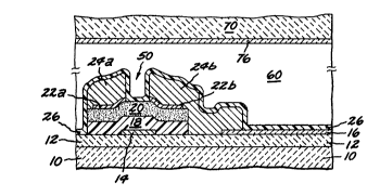
Figure 2 illustrates a portion of a liquid
crystal display device in accordance with the present
invention. More particularly, Figure 2 illustrates
both the upper and lower panel for an LCD display.
130~
RD-18,433
Also illustrated is the physical relationship between
the FET structure and a pixel electrode. In Figure 2
there is shown upper LCD panel 70 which typically
comprises a material such as glass. Also disposed on
the lower surface of panel 70 is a thin coating o~ a
material such as indium tin oxide 76 which acts as a
transparent counter electrode or ground plane elec-
trode. Electrical potential differences appearing
between ground plane electrode 76 and pixel electrode
16 produce optical variations in liquid crystal mater-
ial 60 disposed between these electrodes. It is the
optical effects produced by this potential difference
which cause information to be displayed on the LCD
device. FET 50 and pixel electrode 16 are disposed on
an insulative coating 12 on lower LCD display panel 10.
Coating 12 typically comprises a material such as
silicon dioxide. Panel 10 typically comprises a
material such as glass. In general, panel 70, panel
electrodes 76, pixel electrode 16, coating 12 and panel
10 may all comprise transparent material. This is
particularly useful in LCD displays in which back
lighting is employed to form the desired image.
However, it is only necessary for either upper panel 70
or lower substrate 10, together with its associated
electrode coating, to be transparent.
As indicated above, pixel electrodes 16 are
disposed on one of the LCD display panels. It is also
necessary to connect each pixel electrode 16 with its
associated semiconductor switching element. In the
preQent application, semiconductor switching element 50
comprises an amorphous-silicon-based field effect
transistor which includes gate electrode 14 preferably
comprising titanium. Over gate electrode 14, there is
131~'7~ 6;~
RD-18,433
disposed an insulating layer 18, typically comprising a
material such as silicon nitride. Over insulating
layer 18, there is disposed an active layer of amor-
phous silicon 20. In general, it is desirable to
dispose source and drain electrodes in direct contact
with active silicon material. However, materials such
as molybdenum employed in the source and drain metalli-
zation layer may not form good electrical contact with
intrinsic amorphous silicon. Accordingly, it is
therefore desirable to employ an intermediary contact
metal to facilitate and enhance the electrical connec-
tion to the amorphous silicon. In the present inven-
tion, this includes the utilization of aluminum coat-
ings 22a and 22b for source electrodes 24a and 24b,
respectively. At the same time, drain electrode 24b
and source electrode 24a are fabricated and disposed so
as to provide electrical contact to pixel electrode 16,
as shown. Finally, a layer of passivation material 26,
such as silicon nitride is disposed over the lower LCD
di3play substrate.
It should also be noted from Figure 2 that
gate electrode 14, together with the associated gate
drive lines are in contact with layer 12 as is indium
tin oxide layer 16. If these layers are to be deposit-
ed at approximately the same step in the fabrication
proce~s, the materials chosen for these layers must
exhibit some degree of compatibility. This is particu-
larly true with respect to etchants employed in pat-
terning these layers. Accordingly, the structure and
process of the present invention employs titanium as a
cJate electrode material and indium tin oxide as a
transparent pixel electrode material. Note, however,
~3C~7C~Z
RD-1~,433
that these compatibility problems do not apply to the
ground plane electrode disposed on upper substrate 70.
Figure 3A is a plan view detailing the
physical structure of a switching element 50 and its
associated pixel electrode 16 in the vicinity of the
intersection of gate drive line Gi and data drive line
Sj. For completeness, corresponding structures are
illustrated in cross-section in Figure 3B. In particu-
lar, Figure 3A illustrates the presence of an insula-
tive island principally comprising insulative layer 18
and amorphous silicon layer 20. This island provides
insulation between data line Sj and gate line Gi. It
is also seen that data line Sj may also serve directly
as the source electrode (or the drain electrode in a
reverse situation) for a thin film FET. It is also
seen that gate electrode 14 is preferably provided as
an extension of gate drive line Gi. The gate drive
lines and the gate electrodes are most preferably
fabricated in the same process step and comprise the
same material and in this particular invention, tita-
nium is employed to ensure compatibility with indium
tin oxide pixel electrode 16.
Since the gate electrode is fabricated in an
early process step and is disposed on the underlying
insulative substrate and since the gate insulation
layer also insulates the gate and source electrodes,
the FET structures shown in Figures 2 and 3B are
described as being inverted FETs. This term, however,
applies only to their physical rather than electrical
properties.
Although it may appear that the structure
shown in Figures 1, 2 and 3 is readily constructable,
it must also be appreciated that there are significant
13~
RD-1~,433
material and material etchant compatibility problems
involved in fabricating the structure shown. The
process of the present invention employs materials and
steps which overcome these compatibility problems and
at the same time results in a fabrication process
employing a minimal number of masking operations. The
use of a large number of masking operations is, in
general, to be avoided because of the problems of
device reliability and yield. Accordingly, Figures 4A
through 4J lllustrate various steps in the fabrication
of the device shown in Figures 1 through 3. In partic-
ular, the fabrication process illustrated in these
figures is directed to the production of thin film
amorphous silicon based EET switching element devices
which are compatible with the utilization of indium tin
oxide as a transparent electrode material.
In the process in accordance with the present
invention, an insulative substrate such as glass is
cleaned in order to bring the surface up to processing
quality. Insulative coating 12 such as a layer of
silicon oxide is then provided on one side of substrate
10 to provide a stable surface for further processing.
However, layer 12 can optionally be removed.
Insulative coating 12 typically comprises a
layer of silicon oxide sputter deposited to a thickness
of approximately 1,200 Angstroms.
Titanium is then deposited, patterned and
plasma etched to form the gates of the FETs and the
gate drive lines. The deposition of the gate drive
lines on insulative coating 12 is generally performed
in accordance with conventional masking and patterning
techniques. For example, a layer of titanium may be
deposited by electron beam evaporation to a thickness
~3~'7~ 6'~
RD-1~,433
of approximately 800 Angstroms. This layer is coated
with a resist and exposed to the desired masking
pattern. The substrate is then plasma etched to form
the gate patterns. ~n a preferred embodiment of the
present invention, oxygen ashing of the resist is
carried out at this step and performs a dual purpose,
namely, cleaning off the resist as well as exposing the
gate metal to an oxygen environment which toughens it
prior to plasma etching during island definition.
Figure 4B illustrates the next step in the
process of the present invention. In this step, indium
tin oxide pixel electrode material ~ is sputter
deposited and wet etched. The process step illustrated
in Figure 4B, therefore, represents the second masking
step employed in the present invention. The formation
of the pixel electrodes is performed after the forma-
tion of the gate metallization pattern to avoid expo-
sure to the etchants used to pattern the gate material.
The material of pixel electrode 16 is preferably
deposited by sputter deposition of indium tin oxide to
a thickness of approximately 900 Angstroms.
Figure 4C illustrates the next step in the
process of the present invention which comprises
deposition of insulating layer 18. This layer prefer-
ably comprises silicon nitride which is preferably
formed by plasma enhanced chemical vapor deposition
(PECVD) to a thickness of approximately 1,500 Ang-
stroms. Next, an amorphous silicon layer is likewise
deposited to a thickness of approximately 2,000 Ang-
stroms. For a general description of the PECVD process
cee "Plasma-promoted Deposition of Thin Inorganic
Films" by M. Rand in J. Vac. Sci. Tech., Vol. 16, page
420 (1979). Although it is significantly less
:13(~7a6;~
RD-18,433
desirable, it is also possible to form the amorphous
silicon layer by sputtering and subsequent hydro-
genation. An important aspect of the process of the
present invention is that the next layer of aluminum be
deposited relatively immediately following the amor-
phous silicon deposition in order to achieve reliable
contact. This is very desirable because of oxidation
and contamination of the silicon surface which could
occur otherwise. With respect to the immediacy of the
deposition of aluminum, it is pointed out that this
deposition occur prior to any othsr surface treatment.
For example, it is undesirable to delay deposition of
aluminum for longer than approximately 2 hours if the
substrate surface is exposed to air. Maintenance of
the substrate in inert atmospheres would, of course,
prolong this period of time. Nonetheless, since it is
an object of the pre~ent invention to ensure good
contact with the amorphous silicon material, it is
generally better to deposit the aluminum layer as soon
as practical wlthout subsequent surface treatment. The
depo~ition of amorphous silicon layer 20 is illustrated
in Figure 4D and the electron beam evaporation of
aluminum layer 22 is illustrated in Figure 4E. The
aluminum is typically deposited to a thickness of
approximately 500 Angstroms. The amorphous silicon
layer is preferably deposited by plasma deposition to a
thickness of approximately 2,000 Angstroms. The
resulting structure is shown in Figure 4E.
Figure 4F illustrates that the next step in
the process is the patterning of aluminum layer 22 so
~hat the aluminum layer is cut back from the desired
island structure (more completely formed in subsequent
processing), which is particularly as indicated by
14
13~'7(162
RD-18,433
reference in numerals 20 and 18 in Figure 3A. The
presence of aluminum layer 22 satisfies the contact
requirements, and since it is etched with the indium
tin oxide covered by gate nitride, no "Swiss cheese"
attacX of pixel electrode layer 16 is observed.
Figure 4G illustrates the next step in the
process in which the amorphous silicon and silicon
nitride islands are patterned. This operation repre^
sents the fourth masking step. The mask employed may
be the same mask as that employed to form the aluminum
islands. In order to use the same mask, a double
exposure is made in which the mask is shifted back and
forth in the same diagonal direction twice to insure
greater aluminum removal. However, in general, it is
preferable to employ a separate mask for patterning the
silicon and nitride portions of the island structure.
The purpose of this cut back or set back for the
aluminum layer is to prevent undercutting which could
occur as a result of differential material etch rates
for aluminum and the other island constituents. The
plasma etchant employed to remove the silicon nitride
and amorphous silicon layers do not attack the indium
tin oxide layer.
Figure 4H illustrates the next step in the
process of the present invention in which a layer of
molybdenum is deposited on the substrate. For example,
a 3,000 Angstrom thick layer of molybdenum 24 may be so
deposited. As shown in Figure 4I, this layer is then
patterned using a wet etch with a mixture of phos-
phoric, acetic and weak nitric acids (PAWN) with no
attack of the indium tin oxide material. The PAWN etch
also removes the small amount of aluminum from the
channel between the source and drain pads. The
~3~7~2
RD-18,433
molybdenum source-drain deposition forms a silicide
around the edge of the island which results in gate and
source drain leakage. ~owever, this is eliminated by
plasma etching of the exposed silicon surface (back
channel etching) and the device is then deposited with
a low temperature nitride for protection and passi-
vation of the exposed silicon surface. See Figure 4J.
From the above, it should be appreciated that
the thin film FET and liquid crystal display device and
process of the present invention solves the problem of
electrode contact to amorphous silicon while at the
same time maintaining material composition compatibil-
ity for simplified LCD device fabrication. In particu-
lar, it is seen that the essential parts of LCD device
may be fabricated in a process employing only five
masking steps. It is also seen that the process steps
are carried out in a particular order with specified
materials to ensure that degradation of the pixel
electrode material does not occur. It is also seen
~hat the apparatus and process of the present invention
are such as to be compatible with a large variety of
liquid crystal display systems and with a large variety
of liquid crystal materials. It should also be appre-
ciated that the present invention is one which is
readily fabricatable using relatively conventional VLSI
processing methods so as to enable the reliable and
high yield fabrication of responsive high resolution
liquid crystal display devices.
While the invention has been described in
detail herein in accord with certain preferred embodi-
ments thereof, many modifications and changes therein
may be effected by those skilled in the art. Accor-
dingly, it is intended by the appended claims to cover
13/~ }6Z
RD-18l433
all suc~ modifications and changes as fall within the
true spirit and scope of the invention.
17