Note: Descriptions are shown in the official language in which they were submitted.
1 3 n 1 3 4 7 94024-37/PATENT.AMD/LEH/~Es
--1--
IMPROVEMENTS IN OR RELATING TO DATA COMMUNICATION SYSTEMS
The present invention relates to data communication systems
and more particularly to systems wherein data is received at an
input port of a processor for subsequent use by the processor.
A problem which arises with such systems is that if the
processor is busy on other tasks it may not be possible for it to
perform the system operations necessary for data to be transferred
from the data receiving device hereinafter referred to as a serial
communications controller, to the data buffer memory, either
directly or with the assistance of a direct memory access circuit
(DMA). If the incoming data is being sent at high speed and -the
processor is fully occupied then received information may simply
be lost and the data wi]l then have to be retransmitted causing
delay and inefficient operation of the system.
It is an object of the present invention to provide a data
communication system in which incoming data is extremely unlikely
to be lost due to occupancy of a processor on other tasks.
According to the present invention there is provided a data
communications system including a data communications interface
for allowing data access between a processor and a synchronous
communication link, the processor including a processor bus, the
interface being connected to receive input data from the link at a
rate specified by a synchronous link clock signal provided by the
link, the interface comprising: a serial communications
controller interposed between the processor bus and the link, the
serial communications controller providing controller data and a
~k
7 3 4 79 4024-37/PATENT.AMD/LEH/fs
-l(a)-
request signal, the request signal being asserted when the serial
communications controller is requesting the processor to read the
controller data; storage means, interposed between the serial
communications controller and the link, for receiving and storing
the input data from the link at a first data rate specified by the
synchronous link clock signal, and for transmitting the input data
to the serial communications controller at a second data rate
specified by an output clock signal, the second data rate being
higher than the first data rate, and the storage means being a
first in first out (FIFO) storage device; and control means, for
receiving the request signal and for providing the output clock
signal, the output clock signal being disabled when the request
signal is asserted, the control means thereby controlling the flow
of data from the storage means into the serial communications
controller.
Preferably the serial communications controller is of the
Dual Universal Serial Controller Circuit (DUSCC) type.
In a preferred embodiment a Direct Memory Access (DMA)
circuit is interposed between the serial communications controller
and the storage means to enable the transfer of the data elements
(bytes, words etc) comprising a message, without the intervention
of the processor on an element by element basis, the DMA being
controlled in turn by a processor. Alternatively a processor may
be used directly to control the serial communications controller
and thereby the transfer of data into the memory.
1 3 0 7 3 4 7 94024-37/PATENT-AMD/LEH/fs
Preferably a control means ls provided to control the output
of information from the FIFO storage device to the DMA dependent
on the operative condition of the DMA.
The present invention also provides a method of operating a
data communications interface to forward data received from a
synchronous data communication link to a data processor, the data
to be input to a data processor via a communications controller,
the data communications interface including a first-in first-out
(FIFO) data storage device, a communications controller, and a
control means, the communications controller asserting a request
signal when it contains data to be read by the processor, the
method comprising the steps of: storing data from the link in the
FIFO data storage device at a first clock rate corresponding to a
data communication link clock rate specified by the link, before
the data is passed to the communications controller; reading the
data out of the FIFO data storage device, and, in turn, reading
data into the communications controller, at a second clock rate
which is higher than the first clock rate, the data being read out
of the FIFO data storage device only when the request signal is
not asserted; and reading data out of the communications
controller into the processor after synchronously reading the data
out of the FIFO data storage device.
Embodiments of the present invention will now be described
with reference to the accompanying drawings in which:-
Figure 1 shows in block diagrammatic form a known datacommunication system including a processor which receives and
transmits data from and to a data . . . . . . . . . . . . . . . .
1 3Q73~7
,
communication highway;
Figure 2 shows block diagrammatically the data
communication system of Figure 1 modified ln accordance
with the present invention;
Figure 3 shows block diagrammatically in greater
detail control means for the system of Figure 2;
Figure 4 shows block diagrammatically an alternative
control means for specific data protocol systems;
Figure 5 shows two data protocol systems for receipt
by the embodiment of Figure 4; and
Figure 6 shows block diagrammatically an alternative
data communication system modified in accordance with the
present invention.
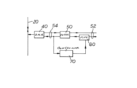
With reference now to Figure 1, a typical data
communication system includes a processor 10 connected via
a highway 20 to various units 30, 32, 34 and to a direct
memory access circuit DMA 40 via a further highway 42. The
DMA 40 is able to transmit and receive status and control
information to and from the processor 10 and to pass
incoming data to a memory 100 for possible future
processing. A serial communications controller 50 is
typically connected to buffer data received from a duplex
data link 52 and is connected to DMA 40 via a simplex
link 54.
In alternative known arrangements shown in dotted
lines the DMA 40 may be omitted. The serial
communications controller 50 may be as shown in solid
lines or may be split into separate receiver and
transmitter sections 50', 50'l as shown in dotted lines.
The transmitter section may be omitted completely since
the present invention is concerned only with the receipt
- of data.
The alternative described systems of Figure 1 are all
able to function satisfactorily provided that data
35 incoming in link 52 can be fed to the memory 100 at a rate
1 3~73~7
--4--
equal to or greater than the rate at which it is received.
If for any reason this cannot be accomplished then a part
of the data received by serial controller 50 (or 50') will
be lost. For the system shown in solid lines, which will
be used hereinafter as an example this can occur when two
received messages abut on the serial highway. There is a
peak in the processor workload at the completion of a
message, where it must ascertain the correctness of the
newly completed message, and then re-configure the system
for the receipt of the next message.
It may be that the processor is busy with another
task when this event occurs, or it could be that the
amount of-time between the adjacent messages is too small
for the processor to perform the necessary work. In the
limit there may actually be a time period of less than 1
data element. DMA 40 may then not be able to gain access
to the memory 100 and may not be able to clear data coming
through the serial controller 50. Serial controller 50
will therefore "dump" the data which will be lost. The
memory 100 will then either receive none of the data or
only a portion and the processor 10 must detect this and
indicate a fault probably requiring re-transmission of the
lost data, or a possible inadvertent reception of corrupt
data will take place.
With reference now to Figure 2 to alleviate this
problem according to the present invention line data input
storage means 60 is provided between the receiver section
of the controller 50 and the link 52. The storage means
is controlled by a controller 70 which receives signals
derived from the DMA's condition to pass data from the
serial controller 50. The storage means 60 therefore
acts as a buffer store to retain received data and to pass
it to serial controller 50 only when it can be processed
by DMA 40. (In the alternative embodiment shown in dotted
lines in Figure 1 the control signals will be derived
1 307347
directly from the processor 10 and the data passed
directly from the receiver section of controller 50 into
the memory 10 or into a register with the processor).
The principle of operation of the invention will now
be described in general with reference to Figure 3 in
which the storage means 60 is a FIFO store. Data received
on link 52 is stored in FIFO 60 at the data rate of the
link for example 2 M bits per second and may be fed into
the input 55 of controller 50 at a higher data rate - for
example 4 M bits per second under the control of
controller 70.
Controller 70 includes the component parts shown
within the dotted line and include a 4 M bit clock
generator 72 which is connected to clock data out of FIFO
into the controller 50 when it is actuated. The
general operation is that clock generator 72 i.s normally
running but may be de-energised by either a signal on line
73 indicating that FIFO 60 is empty or by a signal on line
74 from a unit 56 monitoring the controller to DM~ link 54
indicating that the DMA is unable to receive and process
any further data at that time. A clock start signal may
be given by unit 56 on line 75 when an acceptable
condition is present on the link 54. This restarts clock
generator 72 if any data is still left in FIFO store 60.
Thus incoming data may be stored in FIFO store 60 at the
data rate of link 52 and if DMA 40 is unable to process
the data it will steadily fill up the store. The capacity
of store 60 may be varied to suit the anticipated delay
time during which DMA 40 may be unable to accept data for
transfer to processor 10. The store 60 may, for example,
be 64 bits long or 16 K bits or if a controlled Random
Access Memory (RAM) is used it can be several M bits long.
Once DMA is able to access memory 100 (see Figure 1)
then clock generator 72 may be energised and data will be
fed into controller 50 for subsequent transfer, on demand,
1 307347
--6--
to DMA 40 and then to memory lO0.
With reference now to Figure 4, specific embodiments
are shown related to bit oriented protocol data
transmission and character oriented protocol
transmissions. The message format of these protocols is
illustrated diagrammatically in Figure 5.
Figure 5a shows a character oriented protocol for
example DDCMP (Digital Data Communications Message
Protocol) in which the length of each message can be
determined by decoding the header of -the message. The
header is of fixed length, and contains fields that are
decoded to determine the presence of a length field within
the header, which in turn is decoded to determine the
message size. This is illustrated by the section L in the
message of length Ml. Thus "L" can be decoded to
determine the length of any message and is normally part
of a header section H.
Figure 5b shows a bit oriented protocol (e.g. HDLC)
in which the message M2 is preceded by a FLAG section
comprising a predetermined sequence of bits (e.g.
01111110) and is terminated by the same FLAG sequence.
(There are byte oriented protocols of this general type
such as 'oisync). The system therefore does not know the
length of any message at the start of the message but must
wait until the second FLAG sequence is received to
recognise the end of message M2.
These two types of protocol are dealt with in a
practical system as shown in Figure 4 by including the
circuitry shown in dotted outline for bit oriented
protocol data transmission as now described.
The data is received at the input of FIF0 60 and is
stored therein at a rate determined by the line clock CL2.
The output of data from FIF0 60 is controlled by the
clock CLl. For the invention to work clock rate CLl must
be greater than clock rate CL2 and in a practical
- \ .
` 1 307347
-7-
embodiment a ratio of two to one or greater is preferable.
Clock CLl is generated by two flip flops 80, 82 of D
type and JK type respectively and when running clock CLl
controls both the FIFO 60 and the serial communications
controller 50. The effect of the two flip flops is to
divide an input lock CLO by two to produce an output clock
CLl. The D type flip flop 80 is used to synchronise the
clock control signal from 84, its action is to prevent the
signal on J & K of flip-flip 82 from changing on the 8MHZ
clock edge on which it toggles, thus reducing the
metastable susceptability of the system. The JK flip
flops 82 is controlled by the D type flip flop 80. The
clock ceases to run on receipt of a signal from a NOR gate
84 which changes over the state of D type flip flop 80.
Thus clock CLl is normally running and ceases only when
either there is no further data in the FIFO store 60 or
when the DUSSC or the DMA cannot handle any further data
at that time. If no DMA is present then the clock CLl
will be stopped on instruction direct from the processor.
The detailed operation of the system will now be
described. In order to be able to refer to specifically
generated control signals a particular type of serial
communications controller~nd DMA are referred to by way of
example only. Other types will generate similar control
si~nals which maybe used to control the flow of data
through FIFO 60. If no DMA is used then the signals may
be generated by the processor 10.
The serial communications controller may be of the
SIGNETICS 68562 DUSCC type and data and control signals
are of a type used to control a DMA of the SIGNETICS 68430
type. The signals shown are as follows.
Rx DMA Request This line is asserted to indicate that a
receiver in the DUSCC requires service.
DMA END of frame Typically used to prematurely terminate
a DMA block transfer. This signal also
1 3073~7
--8--
causes the DMA to correctly processs any
buffered transactions that have occurred
prior to the signal.
DMA acknowledge This is a specific signal indicating to
the requesting device that the DMA
transaction has been accepted for
processing and that the device may
transfer the information present at its
output.
10 DONE A signal indicating that the DUSCC has
detected that the current character
being transferred is the last character
of a frame.
The operation of the circuit is as follows:-
Assume the conditions that there is no RX DMA REQUEST
and that there is a data in FIFO 60 which is required to
be processed by processor 10 or stored in memory 100. (For
the present assume the EOF signal is not present its
effect will be explained later).
In this instance NOR gate 84 has only 2 signals, FIFO
O/P register empty, which from the above assumptions will
be false, resulting in 841 being deasserted; and Rx DMA
request on line 842 which is also false since there is no
DMA request yet. The O/P NOR gate (clock enable) 84 is
thus asserted (high). This signal is latched by D type
flip flop 80 on the next low to high transition of CLO.
The action of the JK flip flop is controlled by the Q
output of the D type flip flop. If the output of NOR gate
84 was true on the previous positive clock edge of the CLO
clock cycle then Q of D type flip flop 80 will be set, and
thus J and K of flip flop 82 will be set thus the Q output
of JK flip flop 82 will toggle on the next high to low
clock edge. In this way clock CLl is generated at a
frequency of half that of CLO. This causes JK flip flop 82
to function as a divide by two circuit for clock CLO and
1 3~7347
produce clock CLl which is a clock for clocking data out
of FIFO 60 and also for clocking data into DUSCC 50.
When the O/P of NOR gate 84 is false on the previous
active clock edge of the CLO clock cycle J and K are
clear, causing the Q output of JK flip flop 82 to remain
in its previous state at each clock tick.
If all data is subsequently clocked out of FIFO 60
then FIFO 60 will then assert O/P register empty signal on
line 841 and the output of NOR gate 84 tclock enable) will
be de-asserted thereby de-asserting the D input to D type
flip flop 80, and on the next 8 MHz active clock edge de-
asserting the J ~ K inputsto JK flip flop 82. Thus clock
CLl will effectively stop before the next 4 MHz clock tick
thereby providing an effective "instantaneous" stop for
clock CLl.
If serial data is again clocked into FIFO 60 from
line 52 by the line clock CL2 then the FIFO O/P register
empty signal will be de-asserted indicating data in FIFO
60 and clock CLl will recommence.
When a complete character is present in the DUSCC 50
then Rx DMA REQUEST becomes true and the input(842) is
asserted. This de-asserts the output of NOR gate 84 and
stops clock CLl (as described above). Thus data flow from
the FIFO 60 to DUSCC 50 stops.
If it is configured to transfer data then at some
later time the DMA responds to DMA Request by asserting
DMA ACKNOWLEDGE which serves to clock data out of the
DUSCC 50 into the DMA for subsequent storage in memory
100 .
As this byte of data is clocked out of the DUSCC the
Rx DMA REQUEST becomes false and input 842 of NOR gate 84
becomes false allowing clock CLl to recommence to clock
further data (if present) from FIFO 60 to DUSCC 50.
If the system does not have a DMA then the processor
10 will control the flow of information directly. Thus
1 3n7347
--10--
the processor may provide an equivalent "DMA ACKNOWLEDGE"
signal to the DUSCC to clock information from the DUSCC
directly into the processor 10 or memory 100. This signal
may be derived by interpreting a read from a suitable
memory location as a RX DMA ACKNOWLEDGE.
For character oriented (e.g. DDCMP type) operation
the above process will be continued byte by byte until the
DMA determines that is has transferred a complete buffer
(i.e. a defined series of storage locations of
predetermined length) from the DUSCC to the memory. There
will be no more DMA ACKNOWLEDGE signals produced until the
processor 10 reprograms the DMA. During this period
(which may be very short if the processor is otherwise
idle or long if the processor is very busy) data continues
to flow into FIFO 60. One byte of such data is
transferred into DUSCC 50 and a Rx DMA REQUEST signal is
output. This signal will stop clock CLl and since the DMA
is not ready it will not generate Rx DMA ACKNOWLEDGE so
that the clock CLl will remain stopped. Thus data will
accumulate in FIFO 60.
In bit oriented protocols such as HDLC the
termination comes only from within the message itself. In
this case the DUSCC provides a DONE signal to inform the
DMA that it has reached the completion of a message. Under
these circumstances the DMA has a buffer which is longer
than (or equal to) the maximum message size or a series of
buffers that may be consecutively filled, until the end of
message is reached as indicated by the assertion of the
EOF signal.
In this mode of operation the system works as
described above transferring data from DUSCC 50 to DMA 40
until D~SCC 50 determines the end of a message and asserts
DONE. Flip flop 92 is of the RS type and the output of AND
gate 90 is connected to the set input. When DONE and DMA
ACKNOWLEDGE are both asserted then the output of AND gate
1 307347
~11--
90 also becomes asserted, and this sets the output of flip
flop 92 true and asserts EOF to DMA 40. DMA 40 then
flushes any bytes held internally from DUSCC 50 and
informs the processor 10 that this particular DMA
transaction is complete. The processor 10 is then able to
determine the size of the message from the registers
within the DMA containing the message.
The EOF signal asserted by flip flop 90 provides an
input on line 843 to NOR gate 84 and this sets D type flip
flop input to false thereby stopping clock CLl.
The reason that the DONE signal must be ANDed with
DMA ACKNOWLEDGE is because the DUSCC is a 2 channel
device, with only a single DONE O/P. Thus Rx DMA
ACKNOWLEDE and DONE act to decode the DONE into a DONE -
Rx chan ~ and DONE - Rx chan 1 signal pair.
DMA ACKNOWLEDGE is set false at the end of each
DMA transfer, and since DONE is only true during the ~MA
transfer cycle this S input to RS flip flop 90 only acts
momentarily.
The output of RS flip flip 90 thus remains asserted
until EOF ACKNOWLEDGE from the processor is asserted.
In a subsequent operation the processor is required
to reconfigure DMA 40 to "DMA" a new message from D~SCC 50
into for example a selected memory location in memory 100.
The processor ascerts EOF ACKNOWLEDGE twhich is also a
pulse) to the reset input R of flip flop 92 thus causing
the Q output of 92 to be reset thereby removing the effect
of EOF from the DMA and setting the input (on line 843) to
NOR gate 84 to false thereby allowing clock CLl to
be restarted to transfer further data (if present) from
FIFO 60 to D~SCC 50.
In a system where there is no DMA 40, provision is
made for the processor 10 to have access to the output of
flip flop 92 by a suitable input/output technique so that
the processor 10 is able to pole the output to see when a
~ - 1 3073~7
-12-
frame is complete.
The DUSCC 50 will, when set up to receive, remove any
FLAG or SYNC signals automatically. The reception of FLAG
or SYNC signals will not ascert DMA REQUEST, this not
being ascerted until after receipt of the first non FLAG
or SYNC character.
The reset signal to FIFO 50 may be ascerted at the
commencement of a receive operation to clear FIFO 60 of
all data. Alternatively the data present in FIFO 60 may be
fed to DUSCC 50 which will "dump" the initial data - which
may be garbled - until it receives genuine FLAG or SYNC
signals on which it will act.
The processor 10 will require access to the DUSCC 50
at the end of each frame to determine status information
such as for example CRC (cyclic redundancy check sum)
error. This may be obtained either through the DMA 40 or
direct (via a link not shown) from the DUSCC.
The provision of FIFO 60 in the position shown to
receive data is the preferred embodiment. It may however
be possible to provide the FIFO 60 in a position between
DUSCC 50 and DMA 40. As explained hereinafter this
presents severe problems however for any sophisticated
system and is not therefore preferred.
Most types of serial communications controller
accummulate status information which is obtained from the
incoming data. If the FIFO 60 is placed after the serial
communications controller 50 then such status information
obtained from the incoming data must be stored separately
and thus FIFO 60 would have to be larger and its
interfaces more complex. In its simplest form it would
require to store data and status information separately
but in a parallel form allowing the processor 10 access to
both either via the DMA or directly.
Also in character oriented mode the DUSCC 50
accummulates CRC (cyclic redundancy check) errors and at
-
1 307347
-13-
any stage prior to a CRC being considered good the DUSCC
reports it as bad by ORing this with the accummulated CRC
error. Thus to identify a correct message this status bit
must be cleared by the processor just prior to the last
byte of a message perculating to the top of the DUSCC
internal Rx FIFO. If the external FIFO is on the output
of DUSCC 50 then this operation will not be possible. Thus
extension of -the FIFO by incorporation of a parallel
external FIFO is not possible in this case.
Thus the preferred position for FIFO 60 is on the
incoming side of DUSCC 50.
It should be noted that FIFO 60 operates on incoming
data only~ Transmitted data can be fed through DUSCC 50
or can be fed through a separate transmitter circuit or
can be completely absent in a receive only situation for
example for line monitoring operation.
With reference now to Figure 6 the processor 10 DMA
40 and memory 100 may, as shown be connected by a common
bus 110 which is also connected as shown to the DUSCC 50.
The system can operate as for the system of Figure 4
except that the DUSCC 50 can have direct access to the
memory 100 or the processor 10. When the DMA 40 and
processor 10 are occupied the FIFO 60 is used to store
incoming data which is processed by DUSCC 50 as required
and as explained hereinbefore with reference to Figure 4.
The embodiments of Figures 4 and 6 may be readily
modified to process messages wherein the DMA 40 can
readily keep up except at the end of frames. In such a
case the clock CLl need only be stopped at the End of
Frame (EOF) signal since the DUSCC and D~A can keep up at
all other times. In this case the clock CLl can be
restarted by a signal from the DMA indicating that it has
completed its "End of Frame" processing of the data and is
ready to commence to receive a further message, clock CLl
being again stopped by the end of frame signal at end of
the further messages etc. etc.