Note: Descriptions are shown in the official language in which they were submitted.
307356
Description
PLASMA PINCH SYSTEM
AND METHOD OF USING SAME
Technical Field
The present invention relates in general to plasma
pinch systems, and it more particularly relates to a
plasma pinch system for use in annealing and etching
6emiconductor circuitry.
Back~round Art
~his invention was made with Government support under
Contract No. N00014-85-K-0598 awarded by the Office of
Naval Research. The Government has certain right~ in this
invention.
In the past, there ha~ been several problems
assoclated with the manufacturing procee~ee for integrated
circuits and OEemiconductor chips. For instance, the
conventional use of laser beams for annealing
semiconductor substrates has proven to be a relatively
costly and complex process, and otherwise less than
satisfact~ry. In this regard, trained and skilled
personnel are required to operate the expensive laser
equipment. A much more serious problem relates to the use
of overlapping laser beams, for annealing purposes. Such
techniques have tended to cause a non-uniform annealing of
the substrates. In this regard, certain areas of the
substrateR receive a relatively excessive flux of energy.
In general, the use of a coherent light beam, such as
a conventional laser beam, is sub~ect to diffraction,
<10263-05.212>
-2- ~ 1 307356
which further reduces the performance of the annealing
process. Additionally, an overly extended exposure to the
laser beam can cause micro-cracks or micro-crystalline
damage to the substrate. Thus, the conventional annealing
processes do not produce entirely satisfactory results for
some applications. In this regard, the resulting products
are oftentlmes defective, and an undesirably high re~ect
rate does occur all too frequently. Thus, known processes
frequently produce unwanted 6ide af~ects, are relatively
time consuming, and are costly due to the large number of
re~ects.
Therefore, there is a need for a process and
equipment which prevent, or at least greatly eliminate the
unwanted 6ide affects. Such a new technique should be
relatively efficient and expedient.
Conventional semiconductor etching techniques
generally include exposing a photore~ist-coated sub6trate
to an impinging light beam. However, with the ever
increasing miniaturization of the ~emiconductor integrated
circuitry, the size of circuit details are becoming BO
~mall that they are of a similar order of magnitude as the
size of the wavelength of the impinging light beam itself.
Thu~, the impinging light becomes diffracted, and
irregularitie~ in the resulting product can occur.
Furthermore, due to the relatively low intensity of
nonlaser sources of impinging light, the requlred exposura
time iB extended so as to convey the necessary energy for
use in the etching process. Thus, the etching process is
<10263-05.212~
_3_ 1 307356
not only delayed, but the risk of impurltie~ lnflltratlon
i8 ~ ncreased substantlally.
Therefore, there is a need for an incoherent light
source and a method of using it, whlch not only improves
the anneallng operation~, but which further render the
semiconductor etching processes compatible with modern
techniques. In this regard, the undesirable diffraction
caused by impinging coherent light beam~ would be greatly
reduced, if not minimlzed.
Several attempts have been made to utilize incoherent
light source devices for anneallng and etchlng
semlconductor elements. For example, a surface Epark
technlque has been attempted as a ~ourca of lncoherent
light source. ~owever, the non-uniformity of results, was
a serious problem. Also, the ~ource did not achie~e
sufficiently high temperature~ for efficient light
generation due to problems associated with expansion of
the resulting plasma. Thus, ~uch a technique had only
limited usefulness in modern ~emiconductor manufacturing.
Another prior incoherent light ~ource technique
attempted was the use of an exploding wire. This
technique employed a high current flow in a aonductor to
cause it to explode, thereby providlng the incoherent
light. One serious drawback of the exploding wire
technique was its ~lower repetltion rate, in that the
wirQs must be replaced after each firing. Al~o, the
~ystem did not produce uni~orm resulte.
<10263-05.212>
-4- 1 307356
Yet another attempt at producing an lncoherent llght
source for the ~emiconductor industry, was an approach
known as a plasma focu~ system. Thi~ system employed a
plasma, which was subjected to a magnetlc field for
producing a plasma ~et. The ~et emitted the incoherent
light. However, such technique was not totally
satisfactory, in that the device did not reach
sufficiently high temperatures for semlconductor
manufacturing processes. Also, an inadequata quantity of
ultraviolet light was produced for use in semiconductor
etching or annealing processes.
Therefore, it would be highly desirable to have a new
and improved incoherent light source for the manufacture
of semiconductors, and more particularly, it would be
highly desirable to have a new plasma sy~tem, whlch i8
adaptable for use as a source of incoherent and stabl~
light energy. The pla6ma 6ystem should produce su~ficisnt
energy for use in the etching and anneallng operations ln
the semiconductor industry. The system should al80 be
amenable to cost effective use in the modern mass
production sequences of semiconductor circuitry. The
system fihould be operable at relatively low and thus saeer
voltages. It must be properly focu~able, and it must be
able to be pulsed at a sufficiently high rate of speed to
be useful in the semiconductor industry.
There are, however, several other formidable problems
associated with the use of a plasma as an lncoherent light
source in the manufacture of semiconductors, due to the
~10263-05.212>
1 307356
nature of an ionlzed plasma. Unllke a mQtal or an
electrolyte, a gas free from external influences contains
no free charges to serva as carrier~ of an electrical
current. However, gase~ may be rendered conductlve by
generally causing some of the molecules to become ionized
by the detachment of one or more of their outer electrons.
Some of these detached electrons may then attach
themselves to neutral molecules, to form negative ions,
such that in an ionized gas, both positive and negative
ions, as well as free electrons are usually present. When
the concentrations of the posltlve and negative ions
become appreciable, the ionized ga3 is generally referred
to a~ "plasma".
In most applications, utilizing a hlgh-temperatur~
plasma, such as in a thermonuclear fusion reactor, the
plasma is required to be confined within a suitable
container or chamber, away from its wall~. Such
confinement of the plasma ha~ ~een achleved by various
techniques, which are generally referred collectivQly to
as a "pla6ma pinch".
Plasma pinch sy~tems have been employed for various
applications. For instance, U~S. patent 4,042,848
describes a hypocyclodial pinch device for produclng a
dense plasma at thermonuclear fusion temperatures. U.S.
25 patent 4,406,952 describes a switch for lnterrupting
current using a plasma focus device.
In U.S. patent 4,450,568, there is disclosed a laser
preconditloned plasma pinch, which emits vacuum
<10263-05.21~>
1 3~7356
ultraviolQt radiation, for dissoclating ths molecules of a
photolytic laser medium confined in a chamber. Ths
preconditioning laser beam excites the gas partlcles in
the vicinity of the chamber axis, for defining a
preconditloned channel within whlch the plasma plnch is
formed.
U.S. patent 4,543,231 dQ~cribes a plasma pinch u~ed
in ~usion devices to produce a toroidal pla~ma. In U.S.
patent 4,621,577, there is dlsclo~ed a plasma pinch formed
by a di6charge between electrodes, used for detonating
explosives.
Another ma~or application of the plasma pinch, i~ it~
u6e in X-ray lithography. For example, in U.S. patent
4,424,102, a plasma pinch i8 d~closed and ls used for
reactive ion etching of semiconductor substrates. The
etching proce6s includes the use of magnetic fields in
connection with the plasma pinch. U.S. patents 4,504,964;
4,536,884; 4,618,971; 4,633,492; and 4,635,282 also
di~close various plasma pinch systems u-~able in X-ray
lithography, whereby X-rays are generated by pas~ing a
hlgh current through the pla~ma.
However, none of the prior known plasma pinch systems
havQ been entirely satisfactory for U8Q in ~tching and
annealing sQmiconductors.
Di6closure of Invention
Therefore, it is an ob~ect of the present invention
to provide a new and improved plasma pinch system for use
<10263-05.212>
__.. 3 _ . ~_ . ,,. _ ... ,_.,__,._. _.. ,". ,,.. , ,.:~_ _ ,.. _., .... ... ,.. ... . -
-7- 1 307 3 56
in the etching and annealing operations in the
semiconductor industry.
It is another ob;ect of the present invention to
provide a new and improved plasma pinch system whlch is
amenable to cost effective use in the modern mass
production sequence of semiconductor circuitry.
It i6 yet another ob~ect of the present invention to
provide a new and improved plasma plnch device which is
operable at relatively low voltage~ and is able to be
pulsed for usQ in the manufacture of ~emiconductors.
sriQfly~ the above and further ob~ectA and fQatures
of the present invention are realized by providing a new
and improved plasma pinch system which includes a fluid-
~et plasma pinch devlce, which provides a plasma source
composed of a tenuous vapor preconditioning cloud
surrounding a central narrow flowing fine stream of fluid
under pressure. A discharge device i~ aonneated
electrically to the fluid-jet pinch device for
establishing an electrical current flow through the fluid
~et between a pair of metal electrodes for establishing a
plasma between the electrodes. A method of using the
plasma pinch ~ystem for annealing or etch~ng operation,
includes exposing a semiconductor wafer to the high energy
radiatlon emitted by the pinched plasma and collected by a
system of lenses and/or reflectors.
The use of a fluid stream under pressure that is
surrounded by a preconditionlng vapor sheath for the
plasma pinch formation, produces a highly stable plasma,
<10263-05.212>
1 307356
which i8 suitable for use in the annealing and etching of
semiconductors.
The pla~ma resulting from the use o~ the vapor-
sheath-stabilized liquid-~tream technique of the prQsQnt
invention, i8 uniform and stable, and it radlates energy
of sufficient intensity for use in modern ~emiconductor
anneallng and etching operations. Moreover, the light
beam radiated by the present ~y~tem ls incoherent, and
therefore, the efficiency of the 6emiconductor annealing
and etching processes is greatly lmproved, since the
diffraction problems are eliminated, or greatly reduced.
Additionally, the relatively high energy intensity of the
emitted light, causes the exposure time of the
semiconductor wafer to be reduced, and thus to reduce
greatly or to minimize the possibility of impurity
implantation therein. The present inventive plasma pinch
system is operable at relatively low voltage~ and high
radiative efficiencies, thu~ expanding its ~cope of
application, by reducing insulator deteriorization, and
thus the danger as~ociated with itE u~e.
In the preferred form of the invention, the stream of
fluid i8 a certain liquid, such as decane. In another
form of the invention, the liquid i8 pentane. In yet
another form, the stream of liquld is water.
Brief DescriPtion of Drawings
The above mentioned and other ob~ects and features of
thi~ invention and the manner o~ attaining them will
become apparent, and the invention it~elf will be best
<10263-05.212>
9 1 307356
understood by rererence to the following de~cription o~
the embodim~nt of the invention in con~unction with the
accompanying drawings, wherein:
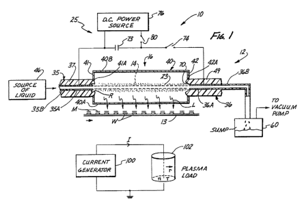
FIG. 1 i6 a diagrammatic view of a portion of a
semiconductor manufacturing process of the present
invention, and employ~ a plasma pinch ByGtem~ which 18
constructed in accordance wlth the pre~ent invention;
FIG. 2 is a graphical representatlon of the numeral
solution for a gas-embedded pinch formation of the present
invention;
FIG. 3 is a 6implified circuit diagram for a kinetic
pinch model of the present invention;
FIG. 4 is a graphlcal representation of the computed
behavior of a 3mm plasma pinch in argon at about 1
atmosphere;
FIG 5 is a graphlcal repre6entation of the computed
behavior of a lmm plasma pinch ln argon at about 0.1
atmosphere;
FIG. 6 i~ a graphical representation of the computed
behavior of a 0.5mm plasma plnch in argon at about 0.1
atmosphere;
FIG. 7 i8 a graphical repre~entation of the computed
behavior of a lmm plasma pinch in argon at about 0.2
atmo~phere;
FIG. 8 i8 a graphical representation of the computed
behavior of a lmm plasma pinch in argon at about 1
atmosphere; and
<10263-05.212>
--10--
1 307356
FIG. 9 is a graphlcal representatlon oP a typlcal
spectlcal power 6pectrum for a blackbody at about
20,000'R to better understand the ~ystem of the present
invention.
Best Mode for CarrYinq Out the Invention
Re~erring now to FIG. 1, there 1~ illu6trated a
plasma pinch 6yatem 10 which ia con~tructed in accordance
with the preaent lnvention, and which i~ adapted for use
in an invention process for manufacturing 6emiconductor
wafers, such as the wafers W carried by a conveyor belt 13
pa6t the ~ystem 10. The illustratQd and de6cribed process
is an etching process, employing a seriQs of conventional
etching masks M having a desired circult configuration
thereon, interposed between the system 10 and the conveyor
belt 13. In thls regard, the plasma system 10 emlts
light L (especially ultravlolet light) which i8 directed
toward the wafers W and the masXs M interposed between the
plasma 6ystem 10 and individual ones of the wafers W, for
serving as a portion of an etching process for the
manufacture of semiconductor chlps resulting Prom the
etching process performed on the wafers W. The remaining
portions of the etching process are conventional and are
not described herein.
The inventive semiconductor manufacturing process
employing the ultraviolet light emitting plasma system 10,
can alao be utilized in the annealing stage of the
manufacture of ~emiconductor chipe (not ~hown). In this
regard, the proce6B i8 similar to the etching process
<10263-05.212>
1 307356
illustrated in FIG~ 1, except that the ma~k~ M ar~ not
employed. Instead, light emitted from th~ sy~tem 10
floods directly onto th~ wafer~ W for annealing purpo~e6.
Thus, the invent~ve ~emiconductor manufacturing process
employs the light emittlng plasma sy~tem 10 for both
etching and annealing portions of the production oP
semiconductor chips.
Con~idering now the plasma system 10 generally
lncludes a plasma ~ource fluid-~et plnch device 12, to
e6tablish a central narrow preconditioned fluid channel
which is generally illustrated in broken line~ at 14, for
the plasma to be formed and pinched therealong, within a
limited volume of a clo~ed chamber 16. The fluid
channel 14 18 initially ln the form of a etream of a
llquid whlch flows under pressure through the chamber 16
that i5 kept at vacuum through the action of a vacuum pump
(not shown). A vapor cloud 23 ~urrounds the liquid
stream, and cooperates therewith to form the main pre-
ionizing driver of the pla6ma sy~tem 10. An electrlcal
di charge device generally indicated at 25 includes a pair
of spaced-apart electrode assemblies 35 and 36 at opposite
ends of the chamber 16, for directing the strèam of liquid
through the chamber 16 and for establishing an electrical
current flow through the preconditioning vapor cloud 23 of
liquid along the channel 14 to establish the plasma.
In operation, a fine stream of liquid flows under
pressure between the electrode aesembly 35 and 36 inside
the chamber 16. The di~charge ~ystem 25 i~ thereafter
<10263-05.212>
.... , _ . _ . .... ... ... . . .. . . . . .. . .
-12- 1 307356
actlvated for delivering a potential of approxlmately
30,000 volts across the elactrodes 35 and 36 to cau~e an
electrlcal current initially through thR vapor cloud 23.
The ~tream absorbs the energy emanating from the non-den~e
plasma 23, and is in turn radiatively heated. The liquid
stream then becomes ionized, and is transformed into a
high-Z dense pla6ma. The generated plasma then conducts
the continuing di~charge electrical current, and produces
high-intensity ultraviolet light. The generated dense
pinched plasma diverts most of the di~charga electrical
current ~rom the surrounding non-dense plasma, and
conducts it along the channel 14 through the chamber 16.
The resulting pla~ma is substantially ~table, and i~
6ubstantially uniform in cross ~ectlon throughout itR
length.
The pinched pla6ma generates an ultravlolet light of
sufficient intensity to anneal or etch the ~emiconductor
wafers W. For this purpose, it i~ desirablQ to generate
recurring discharge pulses by the device 25 at a rate of
about 1-10 pulses per second. Thus, the plasma become~
extinguished and then i5 re-establi~hed repeatedly by the
device 25. In this regard, the foregolng ~teps o~ the
process are repeated each time for re-establishing tha
pla6ma pinch in a recurrlng manner.
Considering now the chamber 16 in greater detail with
reference to FIG. 1, it generally includes an elongated
tubular shell or housing 40, which is hollow throughout
its entire axial length, and which i8 8ubgtantially
<10263-05.212>
-13- 1 307356
uniform ln cross 6èctlonal shapa. The aro~s-ssctional
shape may be circular, oval, or elliptical.
The housing 40 1B substantLally closQd at both of lt~
ends by two end walls 41 and 42, eaah o~ which having
respective central openin~s 41A and 42A for receiving the
front portions of the electrode assemblies 35 and 36 which
are sealed thereto. The housing 40 includes a bottom
wall portion 40A, which is preferably made of guartz,
~apphire, glass, or other suitablQ transparent material,
to permit the llght L to pass therethrough. However, lt
~hould be understood that the bottom wall portion can
alternatively be made of other ~uitable transparent
material. The end walls 41 and 42, and a remaining upper
wall portion 40B may include opaque or reflective lnner
surfaces. Alternatively, the wafers may be placed inside
chamber 40 80 that no window need be employed. In thl~
manner window absorption of vacuum ultraviolet radiation
may be completely avoided.
Considering now the fluid-~et device 12 in greater
2~ detail, it generally includes a preconditioning source 46
of liquid under pressure, for ~upplylng the strOEam of
liquid to the interior of the chamber. A plastic tube 35B
is disposed with a central bore of an electrode 37 of the
electrode assembly 35 and is connected in fluid
communication with the source 46 o~ liguid under pressure.
A metal electrode tube 35A i~ co-axially aligned with tha
plastic delivery tube 35~, to cooperate with a recess R in
the electrode 37 to form an inlet nozzle: to permit fluid
<10263-05.212>
-14- 1 307356
communicatlon between the tube 35B and the lnterlor o~ .he
chamber 16. The tube 35A 1B connected electrlcally to a
dlschargQ capacitor 73 of the di~charge devlce 25. The
stream of liquid under pres~ure flow~ longitudinally
wlthln the chamber 16 a~ a flne (100 pm diameter),
substantially narrow, 6traight and ~ocu6ed stream, and
cau6Qs the annulus of surrounding vapor c;oud 23 to be
formed thereabout.
In the preferred form of the inventlon, the liquid
stream is preferably decane. However, lt wlll become
apparent to those skillQd in the art that pentane or water
can be used alternatlvely. Liquid metal6 ~uch as mercury
or gallium may al60 be employed.
The llquld stream exlts the chamber 16 through the
electrode assembly 36, via a metal tube 36A dl6posed
centrally in a bore of an electrode 49 of the electrode
a6sembly 36 ln a slmilar manner a~ the metal tubs 35A and
the pla6tlc tube 35B of the electrode as6embly 35. A
pla~tlc outlet tube 36B, axlally allgned with the metal
tube 36A, directs the received liquld of the stream to a
sump 60 for dlspo6al purposes. The metal tube 36A is
connected electrically through a switch 74 to the other
terminal of the capacltor 73, the switch 74 being one that
open6 and close~ perlodically. Alternatively, the llquld
~5 ~et itself may act as the 6witch as electrical current may
~low whenever the ~tream ~pans the entire gap between
electrode assemblie6 35 and 36. Thus, the llquld ~et may
be pulsed, periodlcally. In thls regard, the metal
<lOZ63-05.212>
-15- 1 307356
tube~ 3sA and 36A are dispo~ed in con~ronting ali~nment
and are oppositely spaced apart in co-axlal alignment,
with one another to cause ~ub~tantially most of the liquid
particles of the stream 22 to be captured by the electrode
assembly 36.
For the purpose of causing the llquid stream to enter
the chamber 16 at a substantially h~gh velocity, the
llquid flows ln a fina and narrow ~tream, and lt i8 caused
to flow through the chamber 16 under pre~sure.
The Qlectrode assembly 36 generally includes a
funnel-shaped outwardly tapered entranceway 70 to form
with the electrode 49 an outlet collector to help guide
the liquid ~tream into the entrance end of the metal
tube 36A of the electrode assembly 36.
The discharge sy~tem 25 i~ connected to tha
fluid-~et pinch device 12 through the electrode
a~semblies 35 and 36, and in this regard, the
electrode assemblies 35 and 36 serv2 a dual function, as
both channels for the fluid flow, as well as discharge
devices. The electrode bodies 37 and 49 of the respective
electrode as~emblies 3S and 36 are composed of a sultable
non-corrosive conductive material such as brass, stainless
steel, Mallory metal, or a combination of the~e.
The dl~charge system 25 generally includes the
capacltor 73, for storing energy therein, and for
delivering a pul~e of an electrical potential across the
electrodes 35 and 36, via the normally-opened ~witch 74.
While only a single capacitor 73 i5 shown ~chemat~cally,
<10263-05.212>
-16- 1 307356
it will become apparent to tho~e skllled ln ths art that
there may he additional capacltor~ and lnductors (not
shown) to form a bank of such capacitors or a pul~e
forming network (PFN). A power supply 76 i3 generally
connected in parallel with the capacitor 73, via a
normally-opened switch 80 for charging it.
The switch 80 is closed 80 a~ to causQ the power
supply 76 to charge the capacitor 73. The switch 74 i8
opened during the closure time of the switch 30, 60 as to
interrupt the current flow through the electrode
assemblies 35 and 36, while the capacitor 73 i~ being
charged. Once the capacitor 73 is sufficiently charged,
the ~witch 80 i8 opened, and the switch 74 is closed, in
order to causQ the capacitor 73 to be dischargQd across
the electrode 35 and 36 through the vapor cloud 23, and
the stream o~ liquid, for causing the plasma to be formed,
magnetically pinched or constrained ln a ~ubstantially
narrow, linear stable configuration along the channel 14.
While the two switche~ 74 and 80 are described in a
simplified manner for coordinating the firing of the
devices 12 and 25, it should be under~tood that
computerized switching devices such as ignitions,
thyratrons, or spar~ gaps can ba utilized instead, and
that they are opened and closed in a ~uitable recurring
manner.
The plasma emits intense ultraviolet radiation upon
the ionized gas molecules returning to their normal state,
after one or more o~ their electrons have been removed or
<10263 05.~12~
__, . _ ... ..... .. . _ .... .............. ... .. . - .
-17-
1 307356
returned from higher energy levels. Upon the completion
of the discharge of the capacltor 73, the switch 74 i8
opened, while the swltch 80 ls closQd, ln order to cau~e
the capacitor 73 to be recharged, in preparation for a
subsequent pla6ma forming operation.
While in the present lnvention, the plasma pinch is
not embedded within a gas medium, lt should be understood
that, in a gas embedded conflguration, a cold ga~eous
blanket surround~ and stabilizes the plasma pinch, and
insulates it from the inner wall of the housing 40. When
such a pinch is ~ormed in the high-Z gas, its copious
ultraviolet production provokes electrical conductivity in
the surrounding gaseous blanket through photolytic
excitatlon. A conducting sheath may therefor form around
the pinch, and may detract from its ohmic heating rate.
At high den6ities any of these materials may become
optically dense, thereby radiating substantially as a
blackbody.
The liquid stream guided plasma pinch ls a convenient
and a generally well-behaved tool for investigating
diffuse-discharge phenomena. High-Z gases in the pressure
range of 0.02-2.00 atmospheres, generally cause the
plnched plasma to be in a thermodynamlc equilibrium as
well as an efflcient source of vacuum ultraviolet
radiation. A~ a "windowless" ~ource of ultraviolet
radiation, the hlgh-Z gas-embedded plasma pinch becomes a
potent means of photolyzing surrounding gase~. Thus, the
pla~ma pinch system 10 can be employed as a switch, to
<10263-05.212>
-18- 1 307356
control the electrical conductlvlty of the ~heath ~ormed
around the pinch, as pertalning to the control of
thermonuclear nuclear fusion devicQs and the pumping o~
photolytic lasers.
Inductive electrlcal energy atorage i8 presently
being pro~ected as an alternatlva to the traditlonal
capacitor bank for high-energy syetems. Generally, a ten
to one hundred-~old increasa in ~tored energy den~ity may
be realized by the inductiva electrical 6torage
technology. In order to achieve such an advance, a
oigni~icant development in repetltion-rate opening ~wltch
technology is needed, 60 as to enable the extraction o~
energy from the storage inductor.
Analyses of the lnductive swltch problems have
identified the diffuse electrical gas discharge a~ a
plausible current control medium. Conduction may be
provoked through ionization induced by an external source
of radiation. If the electrical fields and gas kinetics
are appropriate for inhibiting the formation of an ara,
then the current flow would be controlled by the external
ionizing source. Openlng the switch is accompli6hed by
lowering the ionization via the ~ource and/or through a
shlft and attachment kinetics. Repetltive pulsQ operation
is facilitated by flushing the current-control medium with
fresh gas for subsequent cycles.
Switches based on the foregoing technology can be
rendered generally practical when each individual process
in the sequance can be accompli6hed ef~iciently. A
~10263-05.212~
-19- 1 307356
~ubstantlally viable sequence i~ the externally-controlled
production of ionization. In general, laser beam, X-ray,
and electron beam sources are substantially limited ln
efficiency. Further, many embodiments o~ switche~ based
on thesQ generator~ are stymied by window transmls~ion and
life limitations as well as repstitlon-rate cooling
i~ues.
A high-denslty, high-Z ga~-embedded plasma plnch can
be a potent ~ource of vacuum-ultravlolet radlation.
Furthermore, the pinch photolytically induces electrical
conductivity in an extended annular ~heath surrounding the
pinch. Thu~, the gas-embedded pinch i~ an attractlve
alternative ~ource of photolonlzatlon for diffusQ-
di~charge opening switches.
Several desirable features are as~ociated with the
use of the pinch as a switch. slnce the gas-embedded
pinch radiates substantially llke a blackbody, it can
become an efflcient source of vacuum ultraviolet energy.
Moreover, the pinch i~ defined or guided by the stream,
and does not requlre a material window. Ths pinch simply
~hares a portion of the photolyzed volume.
The foregoing con~ideration~ ~uggest that a high-Z
ga~-embedded plasma pinch can have application~ both in
the control o~ the fuse-dlscharge switches, and in the
photolytlc excitation of lasers. The cold gaseous sheath
surrounding the plasma pinch damps instabilities, and
consequently optimizes the use of the plasma pinch device
as a 6table source of ultraviolet radiatlon.
<10263-05.212>
-~- 1 307356
The diffusQ-discharge kinetlcs are of considerable
lntQrest with regard to opening swltch concepts and
discharge-excited la~ers. Coupling may be made vla
photolytic proce BeS, and an interpo~ed window may be
avolded ~y explolting magnetlc ~rce~. The followlng
presentation will describe a 6tationary or equllibrium
gas-embedded pinch model, followod by a kin~tlc pinch
model and a bleach wave model.
Enuilibrium Gas-Embedded Pinch
lo Unlike conventional pinche~, where a hlgh-voltage
breakdown esta~ hes the inltlal current flow near the
outer insulating wall of a cyllndrical chamber, and then
proceeds to ionize and to compress the re~t of the gas
toward the chamber axi~, the ga~-embedded pinch of the
present invention utilizes a separate preionlzing finQ ~et
of liquid ~about 100 mlcro-meters) to establish a central
narrow conduction stream 22 about the axis of the chamber,
prior to the application of the di~charge voltage of
30,000 volts.
When the main driver such as the fast llquid
stream iB applied, the di~charged electrical current flows
in a predetermined path therealong, rather than along the
outer periphery of the chamber 16. The ~heath of dense,
cold gas that remains in contact wlth the hot stream 22
provides an e~fective lnertial damper on the growth of
kink instabllities, while thermal conduction lo~ses from
the plnch to its surroundings are kept adequately low.
~10263-05.212~
-21- 1 307356
Analysen o~ the relation between pl~ma pre~ure and
den6ity, pinoh radius, and current profile, may involve
some assumption~ concernlng the conservation of energy and
ma~. The rate of lncrea~e o~ energy in the fuslon plnch
ie a~umed to ba equal to the diffQrence between the
resistive heating and the bremsstrahlung radiation loss,
with contributions from the conduction and line radlation
being relatlvely minimal. Another a~sumption i~ that the
plasma pinch is optically thin. If such as~umptions were
not made, the bremsstrahlung loss rate would have to be
corrected for ~el~-ab~orption, and in the limit, it would
evolve into blackbody radiation.
In analyzlng a high-Z dlffuse-di~charge pinch, a
person skilled ln the art generally encounters parameter
constraints that make the a~sumptlon of optical thickness
of the pinch relatively plausible. The medium itself i~
not hydrogenic, even when ionized, and as such, a large
number of highly absorhing lines will be involved.
Furthermore, as it will become apparant ln the following
de~crlption, the optimum radius o~ the pinch for this
application is more than an order greater than that of tha
fusion pinch.
A~suming that the energy per unit length of pinch i5
added by cla~sical ~oule heating and lost by ~ur~ace
graybody radiation with emis~ivity ~, one obtains the
~10263-05.212>
-22- l 307356
following quantitative relation~ bQtween plasma
parameters, electrical parameter~, and system dimensions:
d
dt (~rr2nkT) ~ I2R - 27rroT~
Where R ~8 the re61~tanc~ per unit length. R 1B
assumed to be the classlcal Spitzer resl~tivity divided by
the column cross ~ectlon, thus:
R ~ 125/~r2T3/2 ( 2 )
It is as6umed that the temperaturs is relat~vely low for
thi~ applicatlon and the ionic charge Z ~ l.
It can be safely a~sumed that the effective pla3ma
temperature in the left side of equation (l) i5 the same
~or ions and ~lectrons, ~ince equipartltion time~ under
present conditions, are very short compared to the
di~charge duration. The density n i8 the ~um of electron
and ion den~ities, and it 1~ as~umQd to be twice the
<10263-05.212>
-23- 1 307356
filling d~nsity of the cold gas. I~ the radiu~ r i8 taken
to ba constant, equation (1) becomee:
dT I2T-3~2 T4
---- ~ Cl ---- c2
dt nr4 nr
where, in mks units and T ln K:
Cl 9 X 10²³,
C2 ~ 8 x 10¹⁵.
The momentum consarvatlon and the aa~umption o~
radial gua~l-equllibrlum (negliqible inertlal ~orce~)
1~ yield an eguation of balance between plasma and magnetic
pressures:
B2
---- a nkT. (4)
2~o
Since:
Bo ~ ~OI/2~r
<10263-05.212>
-24- 1 307356
equation (4), becomes the well-known Bennett relation ~or
plnches:
I2 ~ C3nr2T (5)
where in mks units:
C3 - 9 x 10-16
Equatlone (3) and (5) 3tlll allow for change o~ T
while r i8 constant. I~ however, ~teady-state conditions
are assumed, equation (3) become~:
~ C2
I2 Q __ __ . r3Tll/2 (6)
which, when comblned with equation (5) to elimlnate I2,
becomes:
ClC3 n
Tg/2 . _______ . _ (7)
~2 r .
<10263-05.212~
-25- 1 307356
Assuming that n 1B not a variable, one obtains:
~ ~ r~2/9. (8)
E3y sub~tantiating tha value Or T in equation~ (5~ and
(6), I become~:
I ~ r8/9. (9)
The relation between the discharge resi~tancQ R and
the radiu~ r 1B obtatned from eguations ~2), (8), and (9),
a~ follows:
R - r~l3/9 (lo)
The power P scales a~t
P ~ rl/3 ~ (11)
whlle the axlal electrlcal Pield bQcomes:
. E ~ r~S/9. (12)
Thus, a thlcker pinch re~ult~ in lower temperature~
sllghtly higher total power, lower resistance, and lower
voltage.
For photolytlc application~, the radius will tend, in
the fir~t place, to be limited by coneiderations other
~10263-05.212>
1 307356
-26-
than the above scallng. Most lmportant is the tlme
required for kink instabllities to disrupt the column.
WhilQ lt would seem reasonable to rely on the damping
supplied by the surrounding gas, such damping i8 produced
in part by the transfer of momentum o~ thQ kinking column
to external 6hock waves, which could have harmful effect~
on the gas medium. Thu~, the undamped kink growth rate
should not displace the column by more than its own radius
in the required radiating time.
It i8 easily shown that thi~ growth time, for a
"hlgh p" plasma plnch, 1~ ~u~t the ion sonic translt
tlme over a radlus. Thus, the growth timQ is:
r - r/~T
which, from equatlon (8), becomQs:
r - rlO~g (13)
A largQ radlus 1~ cl~arly beneficial.
ThQ assumption of st~ady state cannot be usQd during
the heatlng pha~e of the pinch, and 80, T~t) and I(t) wlll
<10263-05.212>
-27- 1 307356
now ba examined by combining equations (3) and (5).
Eliminating I, one obta~n~s
dT ClC3T 1/2 ~C2T4
- , (14)
dt r2 nr
or:
dT
-- + FT-1/2 - GT4 (15)
where th~ radius is constant, and where:
F = ClC3/r2,
~nd G = ~C2/nr
are constant3 for a constant radiu~ pinch. For the
following parameters:
0
r ~ 3 x 10~3m, n - 6 x 1024m~3, and ~ ~ 1,
F ~ 9 x 10¹³, and
G ' 4 X 10--7,
a numerical solutlon of equatlon 15 i~ ~hown ln FIG. 2,
both Por T(t) and I(t), obtained by invoking the Bennett
relatlon o~ equation (5). For both T(t) and I(t), a
<10263-~5.212~
-28- 1 307356
nearly lnflnite rate o~ ri~e i~ reguired when T 18 nQar
zero, and thi~ ldeal ~ituation cannot bs met, due to the
llmitation at t ~ 0, to dI~dt ~ VoLJ where VO i~ the line
voltage, and L is the discharye lnductance. However, an
approximatlon to the ldeal ~ituation may be achleved by
making the actual current rl~e time, L/(Zo + R), equal to
about 20 n~, which is that of the idealized I(t).
For a pinch 30 cm long, having r ~ 3 mm, and the
outer current return radius 5 cm, L ~ 170 nh, 80 that R +
ZO ~ 8.5 ohma. For efflcient excitation the pul~e-llne
electrlcal drlver ahould al80 have an impedancQ of about
8 ohms. The pulse-l~ne voltage would then be 320 kV to
brlng the di~charge current a~ymptotlcally to 30 kA.
Kinetic Pinch Model
The foregoing analytical solution for the discharge
developed pertains to a special ~et of circum3tances. It
i8 ueeful in guiding experimental deelgns, as well a~ in
formulating a more ~omplete and more general model. To
develop such a model in which the radlus varie~, involves
a reconslderatlon o~ the equation relat~ng to the
conservation of energy:
dE ~ d[pV/(~-l)] G d[nkT/(7-1)], (16)
where n is the number of particles. The B fields in the
magnetized pla~ma reduce the number of degree~ o~ ~reedom
and the speclfic heat ~ i~ approximately 2, rather than
the customary 5/3. Consequently, by differentiatlng both
~10263-05.212>
-29- 1 307356
~ide~ of the equation (16) with respect to tlme, one
obtains:
dE d
-- ~ -- (~r2nkT) - I2R - 2~roT4~. ~17)
dt dt
Departing now into a kinetic model requirs~ lnvo~lng
momentum balance.
First, one note~ that ther~ is an outward pres~ure
nkT tending to expand the pinch. The magnetic pres~ure
resulting from the current flow I act~ inward to compress
the column. Therefore,
d2r 2kT ~oI2
_ _--G ~ ( 18)
dt2 mir 4~r Nmi
where mi is the lon mass and N - ~r2n is the line
c10263-05.212
~30- 1 3 07 3 56
den~ity. Rewrlt~ng equations ~17) and (18), yiQlds the
following equat~on~:
dT 125 I2T-3/2 T4 2T dr
__ ., ___ . _______ -- ---------- ~ ---- , (19)
dt 2~k Nr2 k N r dt
d2r kT ~oI2
___ , ___ _ ______ _-- . (20)
dt2 mir 2~r N~
As indicnted in F~G. 3, the behavlor 1~ analyzed w~th
a computer code for a current ~ource 100, havlng a
load 102. It3 temporal dependanca ~ assumed to be:
I(t) ~ Io (l-et/r). (21
The ~et o~ equations (19), ~20) and (21) i~ ~olved
with an explicit one and one-half step integration
technique. In this approach, the derivati~e i8 computed
twice for each step, at each 6tep and one hal~ step, in
order to obtaln a hlgh order of accuracy.
Tl, rl, and Vl being the lnitlal valuee o~
temp~rature, radiu~, and veloclty, thQ integration ~or
<10263-95.212>
1 307356
-31-
1,000 ~teps, each ~t apart, i9 performed w~th the
equations:
dT¦ ~t
~n + 1/2 ~ ___ . -- + Tn~
dt n 2
~ t
rn + 1/2 8 Vn -- + rn~
dV ~t
Vn + 1/2 ~ . ~~ + Vn
dT
Tn+l ~ ~~ . ~t) + Tn~
rn+l ' Vn+l/2 (~t) + rn,
Vn+l ' Vn+l/2 (~t) ~ Vn, and
0
t - (n-l) . at, n = 1, 2, 3, ....
Once the temparature history is generated, it i~
stored in a file and retr~eved by another code that
computes the power density from a glven spectral band as a
~unction o~ time. Each temperature i8 used as a constant
in the Planck radiation law which 1~ integrated by
<10263-05.212>
1 307356
-32-
~imp~on's rule. Each Bum i8 stored a~ part o~ the power
hlstory of the pinch and ultimately plotted.
FIGS. 4, 5, 6 and 7 illustrate the computed result~
ror a ranga of initial condltlons. TempQraturQs of tQns
o~ kllodegrees are predicted indicatlng the potential of
the high-Z pinch as an inten~e vacuum ultraviolet source.
The current is given by "x", and the temperature by
llA~ .
FIG. 8 incorporate~ an additlonal dashed curve
indicatlng the temperature as computed by the LANL Global
MHD Model. This model assumes that the plasma channel is
optically thin. Consequently, aven though it i~ a vastly
more sophlstlcated code, its result may be no more valid
than the present predlction ln the case of the high-Z gas
argon. This lends confidence to the utlllzation of the
pre~ent simple code for guiding in the deslgn of
experiments, and in inexpenslvely and rapldly surveying a
broad range of dlffuse-di6charge phenomena in hlgh-Z
gases.
Whlle a partlcular embodlment o~ the prQsent
inventlon has been dlsclosed, it iB to be understood that
various dlfferent modificatlon~ are possible and are
contemplated within the txue splrit and ~cope of the
appended clalms. There is no intention, therefore, o~
limltatlons to tha exact abstract or dl~closure herein
presented.
What is cla~med is:
~10263-05.212>