Note: Descriptions are shown in the official language in which they were submitted.
1 1 3~17~3~
J 1 l PHB33470EP
D~SCRIP~
A ZER0 IF REC~IVER
The prasent inventlon rela~es to a zero IF receiver
including A digital demodulator for deriving amplitude and
frequency inforl~ation.
The zero IF technique is a well known method of i~ple~entinO
a narrowband radio frequency receiver, Ln whic'n substantial parts
of the receiver can be constructed in one integrated circuit.
The filtering function at RF i8 imple~ented at baseband by the
use of low pass filters in two quadrature channels "I" and "Q".
In order to recover the signal Ero~ these two channels, some form
of demodulation is required. Typically amplitude would be
recovered by means of a "square and add" circuit, which is
equivalent to the use of a square law detector in a conventional
superhet receiver. Frequency would be recoveret by means of a
standard FM de~odulator. The dynal~ic range over which the
demodulator is requirad to work is often kept within reasonable
bounds by means of an automatic gain control ~AGC) loop.
However, in some applications, for instance when a short duration
signal, for example a pulsed sine wave, is received there ls
insufficient tllne for an AGC loop to operate over the full
dynamic range oE the receiver, say between 70dB and 8UdB at RF,
or 143 dB to l~OdB after a~plitude demodulation. This makes the
désign of an integrated demodulator circuit very difficult, if
not ilnpossible, using conventional techniques.
~ n obJect of the present invPntion ls to be able to derive
tha Erequency and a~plitude inforiDation from signals having a
relatively large dynalnic range.
According to the present invention there is provided a zero
IF receiver co~prising an input terminal ~or an input signal,
neans coupled to the input terminal for producing frequency
down-convertad in-phase and quadrature-phase signals, first and
second amplifiess having a substantially sinh l transfer
characteristics, the Erequency down-converted signals being
applied to said first and second ampliEiers, respectively, which
,
.
.
`~ 1 7~7~31
1 2 PHB33470EP
produce flrst and second output signals correspondlng
substantially to the logarith~ of the ln-phase and
quadrature-phase si2nals, and de~odulating ~eans, sald
demodulating means com~rising means for determining ehe amplitude
of the input signal by selecting that one of the flrst and second
output si~nals h~vin~ the larger absolute value and means for
deriving the phase from the first and second output signals and
~or determining the ~requency of the input signal relative to a
centre frequency of the receiver from the rate of change o~ phase
of said output signals.
The use of amplifiers having sinh~l transfer characterlstics
enables the dynamic range of the I and ~ signals to be co~pressed
and avoids the use of ~.G.C. Once the dynamic range of the
si~nal has been colnpressed, frequenGy and amplitude infor~ation
can then be derived without the need for circuits of considerable
complexity and thereby enable them to be of a for~ suitable for
fabrication by integratlon.
'Jsing amplifiers having a sinh~l transfer characteristic
e~ectively means that with the exception of signals around zero
volts, the outputs of the amplifiers are the logarithms of the
signals applied to their inputs. This enables the demodulator to
obtain phase and amplitude information relatively simply.
In one embodimel1t of the invention digitising means are
coupled to respective outputs of the first and second amplifiers
for providing dLgitised veriions of the first and second output
signals to the de~odulatil1g means which processes them digitally.
By subtracting the log of the in-phase (I) .Qagnitude from
that of the quadrature (~) magnitude, a function is obtained
~hich represents log of the tangent of phase withln the range O
to 90 de2rees. This information togetber with information about
the p'nase quadrant ~ill define the phase of the slgnal in the
range O to 360 degrees.
Ideally the I and Q signals are in quadrature, so their
instantaneous amplitudes are both 3dB less than the peak value,
whellever their nagnitudes are equal. By choosing the larger of
1 3r'7~31
3 PllB33~1OEP
1 t~e two magnitude~ to represent the signal am?litude one is
assured of being within 3dB oE the correct value. The accuracy
of the amplitude value can be Lncreased by adding correctlons to
the selected magnitude value.
Frequency L~ determined by forming a frame of a plurality of
phase sa,nples and ~irstly using all the samples in the frame to
produce a frequency signal or secondly using subsets of the
samples in the frame to ?roduce other frequency signals. The
frequency samples are supplied to respective inputs of a
frequency selecting circuit. A ~requency selection is made by
producing a further signal indic~tive of the profile of a
plurality of successive amplitude samples fro,n the same frame.
The further signal is supplied to the Erequency selecting circuit
which produces an output frequency signal. In an embodiment in
which there are 4 phase samples per frame the frequency selecting
cLrcuit produces an output frequency signal on the basis of the
follo~ing rules:-
(l) if the amplitude is constant throughout the Erame use
the result of ~aking use of all the phase samples (mode (a)),
(2) Lf the amplitude is not constant throughout the frame
do not use Inode (a),
(3) always use the maxi;num amplitude sample in the
frequency measuring set, except where a constant amplitude
section separates two ri~ing sections,
(4) use a constant amplitude section of the frame where
possible,
(5) where rules (l) to (4) leave a choice, use the first
pair of samples which obey the rules.
In another embodi~ent of the present invention the
demodulating ,neans comprises analogue means for determining the
one o~ the first and second output signals having the larger
absolute value. Such analogue means may coln?rise an analogue
OR-gate having inputs for receiving the first and second output
signals and inverted versions of the first and second output
3ignals, respectively.
,, ~,, ~ , .
.. - . ~
.
' .
-~ ~307~31
4 PHB33470EP
1 rhe present invention also relates to a receiver comprlslng
a plurallty of zero IF recelvers made in accordance wlth the
present invention, each receiver having a local oscillator for
producin~ a dif~erent ~requency with respect to the frequencies
produced by other local oscillators.
The present invention further relates to an interferometer
comprising first and second receiving antennae located at a known
distance apart, a plurality of pairs of first and second ~ero IF
receivers made in accordance with the present invention, each
pair having a common local oscillator for producing a
predetermined frequency which i9 different from the ~requencies
produced by the othar local oscillators, the first receivers of
each pair being coupled to the first antenna, the second
recaivers of each pair being coupled to the second antenna, and
phase difference measuring means coupled to the pairs of
receivers.
The present invention will now be described, by way of
example, ~ith reference to the accompanying drawings, whereln:
Figure 1 is a block schematic diagram of an e,nbodiment of a
~0 receiver made in accordance ~ith the present invention,
Figure 2 illustrates how by setting the local oscillator
frequency FL, a selected part of an overall frequency band of
interest is monitored by a receiver made in accordance with the
present invention,
Figure 3 illustrates the transfer characteristic of the
sinh~1 (or logarithmic) amplifiers used in the receiver shown in
Figure 1,
Figures 4 and S respectively illustrate input and output
waveforms of the sinh~1 a~plifiers,
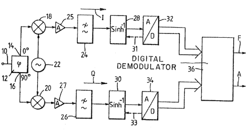
Figure 6 is a block schematic diagram of the digital
demodulator ~sed in the receiver circuit shown in Figure 1,
Figure 7 is a tabular summary of possible amplitude
proEiles, P, produced by the amplitude profile generator used in
t'ne data demodulator illustrated in Figure 6,
Fi~ure a is a block schematic dia8ram of an interferometer
.
,~."~ . - - .
~ 1 J07331
PrlB33470EP
1 usillg two receivers of the type shown ln Figure 1 but having a
com,non local oscillator.
Flgure 9 18 a block schematlc diagram of an embodiment of an
analogue recelver made in accordance with the present inventlon,
Figure 10 illustrates one means by ~hich an analogue
amplitude signal A is obtained, and
Figure 11 ~s a schematic circuit of an embodiment of the
analogue OR ~ate 92 used in Figure 10.
In the drawings the same reference numerals have been used
to indicate corresponding features.
~he zero IF receiver shown in Figure 1 comprises an input 10
which receives an input signal either directly from an antenna or
from a precedin~ amplifier and/or frequency down conversion stage
(not shown). The input signal is applied to a phase splitter 12
which produces a signal (I) which ls in-phase ~ith the input
signal on a first output 14 and a 90 degree phase shifted version
(Q) of the input signal on a second output 16. The in-phase
signal (I) and the quadrature phase signal (Q) are applied to
respective sLgnal paths. The I and Q signal paths are
substantially identical and comprise mixers 18, 20 having first
inputs connected to the first and second outputs 14, 16,
respectively of the phase splitter 12. A local oscillator 22
generating a desired frequency, FL, is coupled to second inputs
of the mixers 18, 20. The frequency FL is chosen to receive
trans,nisslons within a selected narrow band l9 in an overall
wider band 21 of possLble interest (Figure 2). Low pass filters
24, 26 connected to, or embodied in, the mixers 18, 2~ select the
difference frequency components in the mixer outputs. Optionally
ampliflers 25, 27 are provided to amplify the outputs from tne
mixers 18, 20 before they are filtered. The signal components
passed by the low pass filters 24, 26 are applied to respectlve
amplifiers 28, 30 which have a sinh~1 transfer characteristic as
shown in Figure 3. This characteristic which represents:-
Vout ~ A sinh l[B(Vin)]
3~ where A and B are constancs and Vin and VOut are the input and
: .
~ 1 3i~,7~31
6 PIIB3347~EP
1 output voltages, respectively, is een0rally linear ~or very slnall
input volta~es and is substantlally lo$arithmLc for larg~r input
voltages~ The effect of these logarithmic regions is to compress
the amplitude of input voltages. Figure 4 illustrates a sine
wave present at the input of the amplifiers 28, 30 and Figure 5
illustrates the amplitude col~pressed 3ignal at the output. More
particularly for small positive or negative input voltages the
response of each amplifier is linear but for si~nals above a
certain level, each anplifier 28, 30 generates an output which is
substantially equal to lo~(Vin) for positive input voltages, Vin,
and substantially equal to -log(-Vin) for negative input
voltages. These substantially logarithmic voltages represent the
instantaneous voltages on the dB scale. The si2nal outputs from
the amplifiers 28, 30 are digitised in respectlve analogue to
di~ital converters (ADC) 32, 34. In order to distinguish signals
which are positive with respect to the mid-point of ADC input
voltage range frolD ne~ative signals, the positive signals are
encoded with the ~ost significant bit (m.s.b.) equal to a binary
value "l' and the negative sLgnals are encoded with the m.s.~.
equal to a binary value "0". The ADCs 32, 34 set a reference
value corresponding to the mld-point of the input voltage range
of the ADC in the amplifiers 28, 30 by way of the connections 31,
33, respectively, sho~n in broken lines.
The digitised signals are processed i/n a digital demodulator
36 which uses the m.s.b. to determine if a signal is positive or
negative ~ith reEerence to the mid-point of the ADC input voltage
ran8e and operates on the other bits, to produce an amplitude
output A, and a frequency output, F. The digital demodulator 36
will De described in greater detail ~ith reference to Figure 6.
3efore describing Figure ~ in detail the basic principles of
the amplitude and frequency demodulation will be explalned.
Firstly the a~plitude demodulation:-
Assume the signals in the "I' and "Q" channels are represented
by:-
~i = Vmcost~t) (l)
~ 1 3~7~31
7 PHB33470EP
1 Vq = Vmslnt~ t) (2)
where V~ is the amplltude of the input slgnal. Consider first of
all the case where 0~ ~t~lr/2 and take the logarithms oE
equations (1) and (2).
Thus:-
log(Vi) ~ log(V~ log(cos(~t)) (3)
log(Vq) - log(Vm) + log(sln(~J t)) (4)
Since sin(c~t) and cos(~t) are both le~s than 1, equatlons (3)
and (4~ can be rewritten a~ Eollows:-
log(Vi) - log(vm)-Ei
log(Vq) = log(Vn)-E~ (6)
where:-
- Ei ~ -log(cos(3t)) (7)
Eq = -log(sln(~ot~) (d)
The quantlties Ei and Eq are both positive and represent the
differences bet~een the logs o~ the inst~ntaneous voltages Ln the
"I- and 'Q" chann21s and the lop~ of tne signal amplitude. When
~t is~r/4, Vi and Vq are equal and both dlffer from the true
slgnal anplitude by 3dB. For all other values of ~t, either V
or Vq is withln 3dB of the slgnal amplitude. Thus a first
approximation to the signal ampllt~lde can be made simply by
selecting the larger of the instantaneous voltages Vi and Vq.
Thls approximation will have an error of between OdB and 3dB,
depending on signal phase.
~5 The accuracy of the amplitude estimate can be lmproved by
adding ~ correction whlch depends upon the signal phase. This
phase can be derived by subtractlng equatlon (3) from equatlon
(4).
log(tan(~t)3 ~ lo~(Vq)-log(Vi) (9)
The correceion will be zero at phases of O and lr/2 and +3dB
at a phase of lT/4. The correction function is actually Ei or
Eq~ depending upon whether ~t is less than, or greater than
lr/4. The value ls determined fro,n equations (7) or (8), using
the value of ~t derived from equation (9).
So far we have consldered only the range of phases ~here
`:
:
, .. ..,,, ~ -
a7~3l
8 PHB3347~EP
1 bot'a sln(L~ t) and C09(~ t) are positive. To extend the argument
to the more ~eneral case lt ls necessary to use the absolute
values of lnstantaneous volta~e, cos( ~ t) and sin( W t) in
equations (3) and (4):-
lo~(abs(V~ lo~(Vm) ~ loe(abs(cos(G~ t))) (lO)
log(abs(V,~ log(V~) + log(abs(sin(~t))) (ll)
This ls now true for posit~ve and negative lnstantaneous
voltages and any si2nal phase. The coarse estimate of the signal
amplitude, V~n, can still be l~de by selecting the larger of
abs(Vi) and abs (Vq) and the correction functions Ei and Eq are
still valid, if cos(C~ t~ and sin(G~t) in equations (7) and (8)
are replaced by abs(cos(~t)) and abs(sin(c~t)) re3pectively.
Ei - -lo~(abs(cos(~Jt))) (12)
Eq - -log(abs(sin(~ t))) (13)
1S Since only the rnagnitudes of cos(Lat) and sin(C~t) are
required to determine the correction function, it is possible to
use the value of the IDagnitude of tan(C~t) for this purpose.
This can ~e derived from equations (10) and ~11), in a similar
Inanner to equation (9).
log(abs(tan(~t))) - log(abs(Vq)) - log(abs(Vi)) (14)
The functioQs log(abs(Vi)) and log(abs(Vq)) are generated
at the input to the de~nodulator 36.
Secondly the frequency demodulation:
The ,nethod of deriving signal a~plitude described above
involves the calculation of a function of signal phase ~rom
equation (14). This gives a value for the phase which is
restricted to the range 0 to lr/2 radians. The complete phase
can be derived by combining the output of equation (14) ~ith
infonnatioll about the phase quadrant. This is obtained from the
- 30 signs of the outputs of the two sinh~l amplifiers, which preserve
the signs of the "I' and "Q" si~nals. ~nce the phase for each
sample has been obtained, the si~nal frequency can be found Eroin
tne rate of chanze of phase over a number of samples. In the
illustraeed etnbodi~nent the frequency is required to be measured
e~ery four ~alnples. The delnodulator was in consequence designed
1 3~7~
9 PHB33470EP
to derive the Eull stgnal phase for each sample and to use these
phases in groups of 4 samples, in order to generate frequency
measurements. It should be understood the number of samples ln a
group is not restricted to 4 and other numbers may be used.
Referring now to Figure 6, the digital demodulator 36
comprises an input latch 38 ~hich receives the digitised versions
of t;le I and ~ si3nals on inputs 40, 42. The input latch 38 i9
controlled by timlng signals produced by the timing generator 44,
which tlming signals control the clocking-in of the digitised
3ignals ~rom the A to D converters 32, 34 ~Figure l). The
signals, log(abs(Vi)) and log(abs(Vq)), from the input latch 38
are clocked into a magnitude and difference stage 46 in ~hich the
signal amplitude is derived by choosing the larger of the I and Q
signals, independently of its polarity or sign, and then making a
s~all correction, as described above, in the stage 48. The
correction calculated is simply added to the coarse amplitude
value of the larger of the I and Q signals.
The correction effected is based on phase of a signal, that
is (CJt), obtained from equation (14). However this represents
the phase restricted to a 90 degree sector. In order to
determine phase over 0 to 360 degrees it i9 also necessary tu
know in which 90 de2ree sector the phase lies. This ls found
fro,n the signs of the I and ~ signals.
The corrected amplitude signal ls applied to a maximum
amplitude detector 50 which in the illustrated embodiment
operates on frames containing 4 sanples. The detec~or 50
operates by comparing the first and second samples in a frame and
selecting the larger of the two against which the third sample is
compared. The sequence is repeated by comparing the fourth
saDple with the largest of the first three. An amplitude
synchronising stage 52 synchronises the reading out of the
maxi~um amp1itude signal on output A with the reading-out of a
frequency signal on output F. In the present embodiment lf the
clock rate ~s assumed to be 20~Hz then the ou~puts A and F are
read-out at 5MH~ because the signal samples at the inputs of the
1 7 07~3 1
10 PtlB33470EP
demodulator 36 are considered in groups of 4.
In alternatlve, non-illustrated embodiments the amplitude
signal may be determined by calculaeing the average of the four
samples in the frame, by selecting the most common amplitude or
taking the amplitude on or about the pOil1t o~ frequency
measurement.
The corrected amplitude signals Erom the stage 48 are
supplied to an amplitude proflle generator 54. The purpose of
the generator 54 is to examine the shape of the incoming waveform
and to select the appropriate samples rom ~hich to derive the
frequency ,neasurement by way of a Erequency selecting stage 56.
The ~enerator 54 comprises a window comparator which
compares the amplitudes of successive samples within a 4-sample
feame. For each comparison, a comparison output signal is
produced which indicates whether the current sample is the same
(S) as the last, that is it lies within a predetermined window,
or whether it lies outside the window due to thP current sample
being too high (H) or too low (L). For the four samples within a
frame, there a~e thus 3 comparisons and 27 possible combinations
of comparator output. Figure 7 is a tabular summary of the 27
possible profiles, P, together with the comparisons, CF, whlch
describe the respective profiles and the frequency mode, F.M.,
~hich i6 activated in each case.
The size of the amplitude ~indow is controllable by
an exeernal control bus so that the eEfects of noise and
~easurement errors can be accommodated.
Reverting to the magnitude and difEerence stage 46, the
phase of each sample is derived from the difference between the
~agnitudes of the signals in the I and Q channels, which
diEference represents the log of the tangent of the phase angle
Ln a 90 degree (or lr/2 radians) sector. The phase angle
information to~ether ~Lth the sign information is appli~d to a
phase correcting stage 58 which is implemented as a logical
function but alternatively may be i~plemented as a look-up
table. The output Erom the phase correction stage 58 comprises a
..~: i .,
,()7~3 1
ll PHB33470EP
linear phase measurement of the instantaneous signal between
0 de~rees and 360 degrees. These phase measurements are
sequentially applied to a frequency generatlng circuit 60.
The frequency 8enerating circuit 60 calculates the signal
frequency from the rate o~ change of phase within a 4-sample
frame. ~here are four possible modes of operation, depending
upon the amplitude profile detected by the amplitude generating
circuit. The way the circuit ~orks is to generate all four
possible answers as the data arrives and then select the most
appropriate one afterwards, once the amplitude profile is known.
The four modes are:-
a) Making use of all 4 phase samples, generate an averaga
frequency.
b) Use the first pair of phase measurements only.
c) Use the sacond and third p`nase measurements only.
d) Use the third and fourth phase measurements only.
The four modes are supplled by respective lines to the
frequency selecting stage 56. The s~age 56 decides which mode to
adopt as being the frequency F in accordance with some rules.
The rules used to decide which mode ~o choose are (in
hierarchical order of importance) as follows:-
l. If the amplitude is constant throughout the frame usefrequency mode (a) (Figure 7).
2. If the amplitude is not constant throughout the frame do
not use frequency mode (a).
3. Always include the maximum amplitude sample in the
frequency measuring set, except where a constant amplitude
section separates two rising sections (this may correspond ~o a
yulse on pulse situa~ion).
4. Use a constant amplitude section of the frame where
possible.
5. Where rules l to 4 leave a choice, use the first pair of
samples which obey the rules.
Figure 7 sho~s the application of the above rules with the
corresponding frequency measurement modes for eacb of the 27
~,..... .
1 307~31
12 PHB33470EP
possible a,nplitude profiles.
The only ,node ~hich requires phase ambiguity resolution is
frequency mode (a). All other modes use adjacent pairs of phase
measurements9 ~hich must b~ less than 180 degrees apart lf they
are to obey the Nyquist criterion. The phase difference between
ad~acent samples can therefore be converted directly into a
frequency measurement.
The frequency calculation in mode (a) uses the average of 2
frequencies, derived fL~m the first and third phase sa~ples and
the second and fourth pha~e samples respectively. For random,
uncorrelated phase errors with equal variance, this method has a
frequency variance ~hich is almost as good as a least squares
fit. However, it is much easier to implement and in some
situations could give better results, since it gives equal
weighting to all phase samples, rather than biassing the result
ln favour of the first and last phase sample as in the case of
the least squares fit. Ambiguity resolution is also easier,
since each halE of the frequency calculation is done over two
time intervals instead of three. Only one ambiguity resolution
step is therefore necessary and moreover the required information
can be obtained fron differencing circuits used to calculate the
frequencies for modes (b), (c) and (d).
The digital demodulator 36 can be implemented using
combinations of logic elements and hence readily lends itself to
2~
be implemented as a purpose built integra~ed circuit. The
logarithmic amplifiers 28, 30 can be custom built to give a
p$ecewise linear approximation to the curve shown in Figure 3.
Pages 52 and 53 of "Logarithmic A~plification - with Application
to Radar and EW" by Richard Smith Hughes describe a suitable
series linear-limit logarithmic video amplifier technique, which
has been imple~ented in custom integrated circuit form for
bipolar operation in this instance.
The ADCs 32, 34 may comprise any suitable known ADC, in the
embodiment shown in Figure 1 the ADCs 32, 34 comprised Datel
ADC-207 vldeo flash converters. The middle of the range of the
'' :
1 307~31
`1 13 PHB33470EP
output of each of logarithmic amplifiers 28, 30 i9 arranged to
coincide with the midpoint reference of its associated ADC 32,
34 by means of the reference output 3l, 33, respectlvely, of the
ADCs 32, 34, which are coupled to the amplifiers 28, 30. The
maximum anticipated voltage swing of the outputs of the
amplifiers 28, 30 is arranged to correspond to the maximum range
of resistive tappings of the ADC reference chain, that is the
maximum voltage swing is between the positive and negative
reference voltages of each ADC.
One application of the receiver shown in Figure 1 i5 as a
bank of parallel receivers for monitoring many frequencies
simultaneously. A bank of such receivers can be provided with
local oscillators tuned to different frequencies so that
predetermined parts of the spectrum can be monitored for
transmlsslons. The frequency, F, and amplitude, A, outputs of
each digital demodulator are supplied to a central processor (not
shown) which is capable of analysing the ou~puts obtained.
Another application of the described receiver is in
determining the bearing of an unknown signal source by
interferometry. One such arrangement is shown in Figure 8 which
comprises two receivers 62, 64 having a common local oscillator
66 which provides a coherent signal to both receivers 62, 64. At
least the antennae of the receivers are separated by a distance,
d. A signal having a wavelength ~ is received at slightly
different tir~es by the receivers due to the path difference x.
Hence there will be a difference in phase ~ between the frequency
signals produced by these receivers which can be used to
determine the bearing O of the source (not shown) in accordance
with the equation
21Td sin e
~ 3
o
Figure 9 illustrates an embodiment of the invention in which
the I and Q signals are processed as analogue signals to provide
the frequency F and amplitude A signals which may be digitised in
i
~` 1 7~7~31
14 Pt~B33470EP
ADCs 799 81. I~ore particularly a signal on input terminal 10 is
applied to inputs of mi~ers 18, 20. A local oscillator slgnal
FL from the local oscillator 22 is applied to a phase shifter
21 which provides in-phase and quadrature-phase local oscillator
si~nals to the mixers 18, 20. The outputs of the mixers 18, 20
are amplified in amplifiers 25, 27, filtered in low pass filters
24, 26 and the wanted components of the filtered I and Q signals
are applied to the sinh~l amplifiers 28, 30. The log(Vi) and
log(Vq, signals are applied to respective inputs 72,74 of an
analogue demodulator 70. ~u~puts 78,80 of the demodulator 76
provide the analogue values of the frequency F and a~plitude A.
If it is desired to have the frequency F and amplitude A
expressed as digital values then ADC 79, 81 are connected to the
outputs 78, 80, respectively.
One method of obtaining the max~mum ampl~tude signal A is to
use an analogue OR gate 92 (Figure 10). The signals at the
inputs 72, 74, of the demodulator are ap?lied to inputs 84, 86,
respectively, of the analogue OR gate and also are inverted in
inverters 83, 85, the outputs of which are applied to inputs 82,
88, respectively. Using the inverters 83, 85 ensures that it is
the absolute value which is selected as the maximum independent
of sign.
Figure 11 illustrates one embodiment of the analogue OR gate
92. each of the inputs 82 to 88 is connected to the base
electrode of a respectlve NPN transistor 94 connPcted as an
emitter follower. The emitter load of the transistor 94
comprises another NPN transistor 96 connected as a diode, its
base and collector electrodes being connected together. The
emitters of the four transistors 96 are connected to one termlnal
97 of a constant current source 98, the other terminal being
connected to the VEE line. The collectors of the transistors
94 are connected to the Vcc line.
The output of the analogue OR gate 92 is derived from the
base electrode of a diode connected NPN transistor 100 whose
collector electrode is connected by way of a constant current
^ 1 307~31
1 15 P~B33470EP
source 102 to the Vcc Line. The current generated by the
source 102 is set at one half of the value of the current
generated by the source 98. The emitter electrode of the
transistor 100 is connected to another diode connected NPN
transistor 104 whose emitter electrode is connected to the
terminal 97 of the constant current source 98.
In operation the input terminal ~2 to 88 which has the
highest voltage applied to it ~ill cause its associated
transistor 94 to be highly conductive and raises the voltage at
the ter~inal 97. This rise in voltage turns-off all the other
input translstors 94 whose base voltages are lower. The voltage
at the output 90 rises to a level equal to the highest input
voltage, in order to sustain the current flow equal to the
current source 102. In this state, equal currents are flowlng in
~5 the active one of the input transistors 94 and the output
transistors 100, 104. Monitoring the output at the amplitude
terminal 90 thus provides a means of selecting the largest input
voltage. ~oreover the amplitude correction required when neither
I or ~ represents the ma~imum volta~e is provided automatically
by this circuit. When two inputs are almost equal, the current
is shared by two of the four input transistors 94 and the
e~itter-base voltages of these transistors are less than when all
the current flows in one of the input transistors only. Thus the
output voltage is raised to about the input level in this
situation and by careful scaling of the input levels, this offset
voltage can be arranged to track very clGsely with the desired
correction.
: ::
:
~ :: : :
: ;
:
: