Note: Descriptions are shown in the official language in which they were submitted.
- 1 3û7~38
This invention relates generally to stabilizing
idling of an internal combustion engine and, more parti-
cularly, to marine racing applications wherein idle speed
must be reduced to permit gear engagement.
The invention arose during development efforts
in marine racing applications. A high performance or
racing cam shaft requires a higher tllan normal idle speed,
e.g., l,200 rpm. ~owever~ marine transmissions typically
require a l~wer idle speed, e.g., 600 rpm, in order to
shift into gear. When the racing engine is attempted to
be idled at 600 rpm, it breaks into severe oscillation,
with idle speed varying between 400 and 1,200 rpml and
finally not idling at all.
The present invention addresses and solves the
above noted problem by providing an engine idle stabili-
zation timing circuit for an internal combustion engine
having ignition timing means supplying ignition timing
pulses according to a baseline timing curve as a function
of engine speed, said timing circuit including delay means
for variably delaying said ignition timing pulses relative
to a top dead center position of said engine to retard
engine timing from said baseline curvej engine speed res-
ponsive means coupled to said delay means for varying the
relative timin~ delay or said pulses according to engine
speed, acceleration detection means comprising throttle
position responsive means coupled to said delay means for
decreasing said relative timing delay to advance engine
timing for quick acceleration, and engine temperature
responsive means coupled to said delay means for decreasing
said relative timing delay when engine temperature is below
a given value.
In the disclosed embodiment of the invention spark
timing is contxolled by a radical reduction in spark timing
from a normal lO before top dead center to 15-20 after
top dead center and by providing a negative slope timing
curve for self-stabilization. As engine speed increases,
,. . .
`-" 1 ,07~33g
` 2
so does the amount of retard, which in turn reduces
engine speed and thus stabilizes same. Likewise, as
engine speed decreases, the amount of retard decreases
and advances engine timing to thus increase engine speed,
again providing stabilization. A smooth idle around 600
rpm is achieved. At engine speeds above a predetermined
value, e.g., 900 rpm, the timing curve transitions to a
positive slope and at a steeper rate to quickly advance
engine timing and merge with a baseline timing curve.
The timing delay of ignition pulses relative
to a top dead center position of the engine increases with
increasing engine speed along a negative slope to a maximum
delay at a predetermined engine speed, e.g., 900 rpm, and
the relative timing delay then decreses along a steeper
positive slope at higher engine speeds to merge with the
baseline timing curve.
~ ther, the disclosed embodiment of the invention
includes an engine temperature sensitive circuit to reduce
the retard and advance engine timing to the baseline curve
when the engine is cold, and to retard the relative engine
timing from the baseline curve at idle after the engine
reaches a given temperature. An acceleration detection
circuit senses throttle position and ~uickly advances engine
timing to eliminate the retard and enable quic]c acceleration
when called for by throttle advancement. A disabling cir-`
cuit is preferably provided for disabling the acceleration detection
circuit at high engine speeds so that engine timing follows
only the baseline curve. A starting circuit may also be
included to reduce the retard and advance the engine timing
during cranking regardless of engine temperature.
Further features and advantages of the invention
will be apparent from the following description of a pre-
ferred embodiment of the invention wherein:
FIG. 1 is a schematic block diagram of an
engine idle stabilization timing circuit in accordance
with the invention;
`'` 1 307~3~
-- 3 --
FIG. 2 is a graph of engine speed as the
abscissa versus relative -timing advancement as the
ordinate illustrating operation of the invention;
and
S FIG. 3 is a circuit diagram of the invention.
FIG. 1 shows an ignition distri~utor 2 supplying
ignition pulses to an ignition power device 4 which in
turn supplies the ignition timing pulses according to a
baseline timing curve, FIG. 2, for controlling spark
ignition in an internal comhustion engine. FIG. 2
illustrates timing advancement as a
/
: /
/
: /
~ /
~: /
/
/
: ~ /
: ~ /
: ~ /
: /
~ - -- .... ...
, . , ~ .
``` 1 307~3~
function of engine speed and illustrates ba.seline tim-
ing curve 6. This baseline timing curve is typically
pre-~roqrammed into i~nition power device 4, for
example the ~olphin ignition system in ~ercury ~1arine
racin~ applications, ~lercury Marine Part No. 390-7804-
1.
In the present invention, the i~nition timina
pulses either into or out of ignition power device 4
are variably delayed in order to provide idle stabiliz-
ation. In FIG. l, the ignition timing pulses are
~elayed by a timing pulse retard control circuit 8
Drovidinq a variahle delay according to an engine speed
responsive circuit lO. Cranking and warm-up control
circuitry 12 and acceleration detection circuitry 14
are also provided, to be more fully described.
In the preferred embodiment, at engine speeds
up to about 900 rpm, FIG. 2, the ignition timing pulses
are variably delayed relative to a top dead center
position of the engine to retard engine timing from
baseline curve 6. The relative timing delay increases
with increasing engine speed as shown along dashed line
negative slope 16. The relative timing delay is at a
maxi~um at inflexion point 18 at 900 rpm engine
speed. The relative timing delay thus increases with
~r
increasing engine speed up to such predetermined
speed. At engine speeds higher than 900 rpm, the rel-
ative timing delay decreases with increasing engine
speed along positive dashed line slope 20 which is
steeper than negative slope 16. The decreasin~
relative timing delay along steep slope 20 merges with
the baseline timing curve 6 at about 2,200 rpm, the
steep slope 20 providing a gradual mer~ing transition
; ~ with the haseline timing curve to eliminate surging.
Idle stabilization is provided as ~ollows.
~ 35At speeds below 900 rpm, e.g., 600 rpm, an increase in
:~ :
.",,,,:,.
1 ;C7c~38
engine speed increases the relative timing delay, i.e.,
rightwardly downwardly along neqative slope 16, which
increased ~elay ~urther retards engine timing, which
further retarded timing 510ws en~ine speed, hence pro-
viding self~stabilization. Likewise, a decrease inengine speed decreases the relative timing delay, i.e.,
leftwardly up~ardly along negative slope 16, and thus
advances engine timinq, which advanced timing increases
engine speed, hence providing self~stabilization. As
above noted, t~e rate of delay increase with increasing
engine speed up to the predetermined 900 rpm speed is
less than the rate of delay decrease with increasing
engine speed above the predetermined 900 rpm speed such
that the slope 20 of the latter is steeper than the
slope 16 of the former, with the slopes meeting at the
maximum delay 18 corresponding to the predetermined 900
rPm spee~.
Timed ignition is provided relative to a top
dead center position in a cycle of revolution of the
engine. In the preferred embodiment, the idle stabil-
ization circuitry delays the ignition pulses by a fixed
absolute time interval up to a predetermined engine
speed such as 900 rpm. Such fixed absolute time
interval becomes a greater percentage of the time
needed for the engine to complete a cycle of revolution
as enqine speed increases up to the predetermined
speed. That is, at low engine speeds, the period or
time for one revolution is greater, and the ~ixed delay
::
interval is a small fraction thereof. ~s engine speed
increases, the perio~ or time for a revolution is
smaller, and the fixed delay interval becomes a greater
fraction thereof. ~ence, the fixed ahsolute time delay
interval ~ecomes a greater number of degrees after top
dead center as engine speed increases. Thus, the delay
~35 of the ignition timing pulses relative to the top dead
,.. . .
. ~ .
,a7~3~
-- 6 --
center ~osition increa.ses alon9 negative slope 16 with
increasing engine speed up to the predeter~ined speed,
to increasingly retard enqine ~iming from the baseline
curve to a maximum delay at transition point 18 at the
~redetermined speed. ~t speeds above the predetermined
speed, the ahsolute time interval of delay is decreased
with increasing engine speed to decrease delay of igni-
tion timing pulses relative to the top dead center
position, to advance engine timing along slope 20 to
~erge ~ith the baseline curve.
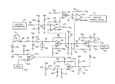
Referring to FIG. 3, ignition pulses from
distributor 2 are supplied through resistor 22 to the
plus input as a comparison input of comparator 24~ A
pair of diodes 26 and 28 are provided in series between
ground and a fixed voltage source V~D and provide volt
age clipping and noise suppression. Resistor 30 and
capacitor 32 provide an RC timing circuit. The minus
input of comparator 24 is used as the reference voltaqe
input and is connected to node 34. The output of
comparator 24 is tied through resistor 36 to the volt-
age supply VDD and is also fed back through diode 38 toprovide positive switching of comparator 24. When the
incominq ignition pulse from distributor 2 is low,
capacitor 32 discharges through resistor 22. When the
incoming ignition pulse transitions high at a leading
edqe, capacitor 32 càn no longer discharge through
resistor 22 and instead is charged from VDD through
resistor 30. When the voltage at the comparison plus
input of comparator 24 rises ahove the voltage at the
~inus reference inpu~, or above a given threshold value
relative thereto, the output of comparator 24 goes
; high. The leading edge of the ignition timing pulse is
delayed by the RC time constant of RC timing circuit
30, 32.
1 J~7~38
The output of comparator 24 is connected to
the minus input as a comparison input of intermediate
com~arator 40. The plus input of comparator 40 is used
as the reference input and is connected through
resistor 42 to a voltage supply VD which is less than
VDD and is obtained from volta~e divider network 56,
58, to be described. ~hen the output of comparator 24
qoes hi~h, such high state at the minus input of
comparator 40 causes the output of comparator 40 to qo
low. Re.sistor 44 and capacitor 46 connected between
the volta~e supply and ground provide a second RC tim-
ing circuit, Capacitor 46 is discharged by the low
state of the output of comparator 40.
The output of comparator 40 is connected to
~he minus input as a comParing input of an output com
parator 48. The plus input of comparator 48 is used as
the reference input and is connected to node 34. ~hen
the output of intermediate comparator 40 goes low and
discharges capacitor 46, the voltage at the minus inPUt
of comparator 48 droPs below the volta~e at the refer-
; ence plus input, or lower than a ~iven threshold value
relative thereto, and the out~ut of comparator 48 goes
~; hi~h. The outPUt of comparator 4R is connected to the
iqniton power device 4, for example the above noted
; ; 25 Dolphin iqnition system in a r1ercury r1arine Merc
Cruiser line. The leading positive-going edge of the
; iqnition pulse ~rom distributor 2 has thus been pro-
cessed through input comparator 24, intermediate
comparator 4~ and output comparator 48 to provide a
30~ leadin~ositive-going ignition pulse edge to ignition
power device 4 which has been delayed by RC timing
circuit 30, 32.
When the ignition pulse from distrihutor 2
transitions 15w at its trailing edge, such low state
discharges capacitor 32 substantially instantaneously
:: :
: ,.,, - - '
1 -')G7 ~38
through resistor 22. This low state causes the voltage
at the com~aring plus in~ut of comparator 24 to drop
helow the voltaqe at the minus reference input from
node 34, or helow a qiven threshold value relative
thereto, and the output of conparator 24 goes low.
This low state presents a low voltage at the minus
comparinq in~ut of comparator 40 less than the voltage
at the reference plus input, or less than a given
threshold value relative thereto, and the output o
comparator 40 thus goes high. The hi~h state of the
output of comparator 40 prevents capacitor 46 from
discharging, and capacitor 46 instead is charged by the
voltage supply through resistor 44. The charging time
of capacitor 46 delays the rise in voltaqe at the minus
com~aring input of comparator 48, as determined b~ the
RC time constant, and when such voltaqe increases above
the voltage at the plus reference input, or above a
qiven threshold value relative thereto, the output of
comparator 48 transitions lowO Hence, the negative-
going trailing edge of the ignition pulse from
distributor 2 has been processe~ through the
comparators and then output to i~nition po~er device 4
as~a trailin~ edqe delayed by RC timing circuit 44, 46.
The amount of delay of the lea~ing and trail-
2~ ing edges o the ignition ~ulses is determined by the
voltage at reference node 34. The lower the voltage at
node 34, the less the delay. A low voltage at refer-
ence node 34 presents a low voltage at the minus refer-
ence in~ut of com~arator 24, which in turn means that
the voltage a~t the plus comparison input o comparator
24 does not have to rise as high until it reaches the
volta~e at the minus reference input, or a given
threshold value relative thereto, hence causinq the
output o~ comparator 24 to transition high. Likewise,
~ 35 a low reerence voltaqe at the plus reference input of
:~ ` ' :
1 3G7~3~
output comparator 48 means that the voltaqe at the
~inus co~arison input of comparator 48 does not have
to rise as hiqh to reach the voltage at the plus refer-
ence input, or a qiven threshold value relative
thereto, thus causin~ the output of comparator 48 to
transition sooner. Increasin~ the volta~e at node 34
increases the reference input voltage to the input and
OUt~llt comparators 24 and 48 which in turn requires a
lonqer ti~e delay before the respective capacitors 3?.
and 4fi are char~ed to the switchin~ threshold value for
the resPective comparator, hence increasing the delay
of the respective leading and trailin~ edge of the
ignition pulse. Thus, th~e lower the voltage at node
34, the more advanced the spark timin~, and vice versa.
An engine sDeed responsive circuit is prov-
ided by a tachometer 5~ outputtin~ a DC voltaqe as a
function of engine speed and a differential amplifier
52 receiving the speed responsive volta~e through
resistor 54 at its minus input as a comparison input.
The plus input of differential amplifier 52 is used as
the reference input and is connected to the voltage
supply through the voltage divider network provided by
~resistors 56 and 58 and filtered by capacitor 60. The
output of differential amplifier 52 is connected
25~ throu~h resistor 62 to node 34 and through feedback
resistor 64 to its minus input for controllinq the
gain. In the preferred embodiment, the offset of the
differential a~plifier is set so that the tacho~eter
siqnal does not come into play until about 900 rpm.
The oUtPUt of differential a~plifier 52 is normally
; hi~h when the en~ine speed is below 900 rpm and the
tach voltaqe at the minus co~parin~ input of differen-
tial amplifier 52 is less than the reference volta~e at
the plus reference input of differential amplifier 52.
.
::
,. ,
:: .
.
' 1 337~3~
-- 10 --
The nor~ally hiqh state at the OUtpllt of
differential ampli~ier 52 prevents capacitor 66 from
dischar~in~ such that a normally hi~h voltage appears
at node 34 set by the voltaqe divider network provided
by resistors 68 and 70. This normally high set voltage
provides a fixed reference voltage to the reference
inputs o~ comparators 24 and 48 to provide the above
noted ~ixed a~solute time interval of delay of the
leading and trailing edqes of the iqnition pulse.
~hen the enqine speed exceeds 900 rpm, the
volta~e at the minus comparing input of differential
a~plifier 52 ri~ses above the volta~e at the plus refer-
ence input of differential amplifier 52, or above a
qiven threshold value relative thereto, and the output
of dif~erential amplifier 52 goes low. This lo~ state
of the output of differential amplifier 52 sinks
current from capacitor 66, thus reducing the vcltage at
node 34, hence reducing the relative timing delay of
the ignition pulses and advancing engine timin~. The
output of differential amplifier 52 rapidly ~oes low to
provide the steep slope 20 in Fl~. 2. The steeper the
slope, the more gradual the mer~er with the baseline
timing curve, and hence the gain of diferential am~
fier 52 is set accordingly. Zero voltaqe at node 34
~eans no relative timin~ delay and hence the engine
timing follows the haseline curve 6.
A second differential amplifier 72 has its
minus input as the comparison input connected throu~h
resistors 74 and 76 and voltage clipping diode 78 to
30~ the volta~e supply. A capacitor 80 is connected
between ground and the junction of diode 78 and
resistor~76. A temperature responsive element 82, such
as a neqative temperature coefficient thermistor sens-
inq engine temperature, is connected between ground and
3' the junction of resistors 74 and 76. The plus input of
: ::
:~
1 707~3~
-- 11
differential amplifier 72 is used as the reference
input and is connected to the volta~e supply throuqh
the voltaqe divider network provided by resistors 84
and 8h. The output of differential amplifier 72 is
connected to node 3~ and also fed back through resistor
~8 to the minus input to control qain. ~hen the engine
is cold, the resistance of thermistor 82 is high, and
the voltage thereacross is high as provided by the
voltaqe divider network provided by resistor 76 and the
resistance of thermistor 82, which hi~h state at the
minus comparing input of differential amplifier 72
causes the output of diferentia] amplifier 72 to be
low. This low state sinks current and discharges
capacitor 66 such that node 34 is low, hence providing
little or no relative ti~ing delay, and advancing
engine timing to the baseline curve. r~aximum spark
advance is thus provided durinq warm-up.
As the engine warms up, and its tem~erature
increases above a given value, the resistance of
thermistor 82 decreases, which reduces the voltage
thereacross, and hence reduces the voltage at the minus
comparing input of differential amplifier 72. ~hen the
voltage at the minus comparing input of diferential
~ amplifier 72 drops below the reference voltage at the
plus reference input of differential amplifier 72, or
below a ~iven threshold value relative thereto, the
output of dif~erential amplifier 72 goes high. This
high state at the output of differential amplifier 72
; prevents discharge o~ capacitor 66, and hence increases
; 30 the voltage at node 34, which in turn provides the
above noted relative timing delay along slopes 16 and
20, FIG. 2, as controlled by differential amplifier 52
according to engine speed. Capacitor 80 provides a
gradual transition from advanced to retarded timing
3' when the voltaqe siqnal at diode 94 is removed either
.' ' ' .
1 ~3703~
- 12 -
by the ther~ostatic switch 90 or start switch 9l.
Capacitor 80 discharges slowly throu~h thermistor 82,
and during such slow discilarge, capacitor 80 holds up
the volta~e at the minus comparin~ input of differen-
5~ tial amplifier 72, to in turn provide a slow ~radualtransition of the output of differential amplifier 72.
During crankinq, when starter switch 91 is
manually closed by the operator, startinq voltage, for
example from a startin~ battery 92, is supplied through
diode 94 and resistor 96 and then through resistors 76
and 74 to the minus comparillg input of differential
amplifier 72 to thus provide a high state thereat
whereby the output of differential amplifier 72 is low
and hence node 3~ is low, and hence maximum spark
advance is provided during crankin~, regardless of
engine temperature. Thermostatic switch 90 is respon-
sive to en~ine temperature and is closed when the
engine is cold to ~hus complete a circuit from battery
92 and provide maximum spark advance. Thermostatic
swtich 90 opens when the engine temperature rises above
a given level, to enable the above noted retard. In
the preferred embodiment, thermistor 82 is selected
such that its low resistance state does not
sufficiently decrease the starting voltage at the minus
~5 comparing input of differential amplifier 72 below that
at the plus reference input, or below a given threshold
value relative thereto, such that even if the enqine is
cranked for restart when hot, maximum spark advance is
still provided during such restart cranking.
A third differential amplifier 98 has a plus
comparing input connected throu~h a differentiating
network, provided by capacitor lO0 and resistor 101, to
a throttle position sensor 102 in the form of a potent-
iometer connected to the supply voltage. When the
throttle~ IS advanced to accelerate the enqine, wiper
. . ~ , :
: : .
1 307~38
arm 104 o~ the potentiometer moves upwardly such that
the divided voltage thereat increases. Diode 106 pro-
vides clipping and Drotection. The minus input of
,li~ferential amplifier 98 is used as the reference
'~ input and is connected to a reference voltaqe source
which is low below a given elevated engine speed, to be
described. The output of di~ferential amplifier 98 is
connected throuqh resistor 110 and diode 112 to the
minus comparing input of differential amplifier 52, and
is also tied to the voltaqe supply throu~h resistor 114
and filtered by capacitor 116, and is also fed back
throuqh resistor 118 to the minus input to control
gain. In response to throttle advance calling for
rapid acceleration, wiper arm 104 moves upwardly and
the voltage at the plus co~parin~ input of differential
; amplifier 98 rises rapidly above the reference voltage
at the minus reference input, or above a given
threshold value relative thereto, and the output o~
differential amplifier 98 rises, whereby the minus
comparing input of differential a~plifier 52 rises in
voltaqe levell and hence the output of di~ferential
amplifier 52 at no~e 34 goes low, which in turn reduces
the relative timing delay and advances the timin~ to
enable~quick acceleration.
25~ The acceIeration detection and timing advance
` iS disabled above another higher predetermined engine
:: :
sReed, e.q., 3,500 rpm where there is no need ~or such
circuit or its retard or advance. A fourth differen-
tial amplifier 120 has its plus comparin~ input con-
~ nected throu~h resistor 122 to tachometer 50. Theinus input of di~ferential amplifier 120 is used as
the reference input and is connected to the voltage
su~ply throuqh the voltage divider network provided by
resistors 124 an~ 126. The offset is selected so that
the tach voltage does not come into play untll about
:~ :
: ~
~: .
1 307~3~
-- 1~
3,50n rPm in the preferred embodi~ent. At engine
speeds below 3,500 rp~, the volta~e at the plus compar-
ing input of differential amplifier 120 is below the
voltage at the minus reference input of differential
amplifier 120, or lower than a given threshold value
relative thereto, and the output of differential ampli-
fier 120 is low. The output of differential amplifier
120 is connected throuqh diode 128 to the minus refer-
ence input of differential amplifier 98, and includes a
hias resistor 130. The minus reference input of dif-
ferential amplifier 9~ is thus low at engine speeds
below 3,500 rp~. When the engine speed increases above
3,500 rpm, the voltage at the plus comparing input of
differential amplifier 120 rises above the voltage at
the minus reference input of differential amplifier
120, or above a given threshold value relative thereto,
whereby the output of differential amplifier 12~ goes
high and presents a high state to the minus reference
input of differential amplifier 9~ which is higher than
2~ any voltage at the plus comparing input of differential
amplifier 9~, regardless of the positlon of potentio-
meter 102, whereby the output of differential amplifier
9~ stays low and is disabled, and hence differential
amplifier 52 is controlled solely by the tach voltage.
2S It is recognized that various equivalents,
alternatives and modifications are possible within the
scope of the appended claims.
.
:
: :
,, ' .