Note: Descriptions are shown in the official language in which they were submitted.
~L3~7~?4~
TRANSMITTER WITH AN IMPROVED SPAN ADJUSTMENT
BACKGROUND OF_THE INv-ENTIoN
1. Field of ths Invention
This invention relates to a two-wire process
s variable transmitter with an adjustable span.
SUMMAR~ OF THE INVENTION
This invention relates to a transmitter which
senses a process variable and provides a two-wire
output representative of the process variable. The
process variable can comprise a pressure, temperature,
flow or other process variablle. The transmitter
receives a span adjustment which adjust~ the span of
the transmitter's ou~put. The transmitter comprises
sensing means which sense the process variable and
provide a sensor output representative of the process
variable. The transmi~ter further comprises
span-controlling means coupled to the span adjustment
and the sensor output. The span-controlling means
control the two-wire outputO The span-controlling
means further comprise first impedance means for
adjusting the span. The first impedance means have a
first impedance which increases responsive to a span
adjustment increase. The span-controlling means
` further comprise second impedance means for adjusting
the span. The second impedance means have a second
impedance which decreases responsive to a span
adjustment increase. The first and second impedance
means are coupled to the sensor output such that the
two-wire output has an increased resolution as a
function of span adjustmentO The transmitter further
comprises output means which couple to the
span-controlling means. The output means provide the
two-wire output.
In a preferred embodiment, the transmitter
further comprises adjustment means for receiving the
span adjustment. The adjustment means are coupled to
~1 .
.
,
: ' ` :-
~"i.,, ~
.~
13~7~
.
-2-
the span-controlling means. The span adjustment is
coupled through the span adjustment means to the
span-controlling means to control the magnitudes of the
first and second impedances. In a further preferred
embodiment, the span-controlling means further comprise
amplifier means having an input and output coupled to
the first and second impedance means for amplifying the
sensor output. The first impedance means can be coupled
between the amplifier's output and the output means to
provide a feedforward control of the transmitter's
span. The second impedance means can be coupled between
the amplifier's input and output to provide feedback
control of the amplifier's gain. Both the feedforward
and the feedback controls of span affect the output
resolution. The two effects on output resolution
combine to give the desired output resolution over a
selected turn down ratio. The transmitter is thus
useful for sensing over a wide turn down ratio range
and the undesired resolution limitations of the first
and second impedance means are substantially overcome.
In a further preferred embodiment, the first
and second impedancP means together comprise a variable
resistance, such as a potentiometer. The potentiometer
has an adjustable tap which is coupled to the
amplifier's output to provide the desired high
resolution. In yet another preferred embodiment, the
two-wire output is a 4 to 20 milliampere current which
energizes the transmitter. The sensor means can
comprise a capacitive pressure sensor.
. . ~- ... ..
~3~94~
BRIEF DESCRIPTION OF THE DRAWINGS
FIG. 1 is a part schematic, part block
diagram representation of a PRIOR ART transmi~ter wi~h
a span adjustment.
FIG. 2 is a graphical representation of
resolution factor as a function of gain for both a
prior art transmitter and a ~ransmitter made according
to this invention.
FIG. 3 is a part schematic, part block
diagram representation of a transmitter according to
this invention.
FIG. 4 is a schematic diagram of a capacitive
pressure transmitter made according to this invention.
DETAII.~D DESCRIPTION OF THE PREFERRED EMBODIMENTS
An exemplary PRIOR ART transmitter is shown
schematically at 10 in FIG. 1. A process pressure P
couples to a sensing means 20 which capacitively senses
the process pressure P and provides a sensor output Vs
on conductor 22. Tbe output Vs on conductor 22 has an
amplitude which is representative of the sensed
pressure P. A non-inver~ing input 24 of operational
amplifier 26 senses the sensor output. The output 28
of operational amplifier 26 is coupled via conductor 32
to terminal 1 of span adjustment potentiometer 34.
Terminal 2 of span adjustment potentiometer 3~ is
coupled to a fixed reference potential (DC common) 36.
The wiper of the potentiometer, terminal 3, is
connected to an inverting input 38 of operational
amplifier 26 via conductor 42. The potentiometer 34
presents a resistance Rl between terminals 1 and 3 and
presents a resistance R2 between terminals 3 and 2.
- The potentiometer has a resolution associated with it
' "'' :: :
~3~4Cl
--4--
that is determined by the smallest increment of
resistance--"delta R~ that can be practically adjusted
with the potentiometer. The resolution (delta R/(Rl +
R2)) of the potentiometer is the ratio of the smallest
practical increment of adjustment "delta R~ of the
potentiometer to the total resistance (Rl ~ R2) of the
potentiometer.
The amplifier 26 and the potentiometer 34
comprise a gain stage 4~ which receives the sensor
output Vs and provides a span-adjusted output Va. The
gain of the output stage is th,e ra~io of ldelta
Va/delta Vs) which is controllled by the potentiometer
adjustment according to the formula:
Gain = delta Va = (Rl ~ R2) /R2~ E~. 1
delta Vs
where delta Vs is a change in the magnitude of the
sensor output and delta Va is a corresponding change in
the span-adjusted output.
The span-adjusted output Ya i5 applied to an
output circuit 46 which provides a 4-20 mA output
signal 48 to a two-wire current loop comprising a power
source 52 and a load impedance 54 coupled together in
series. The transmitter's span is a ratio of a change
of output current to a change of input pressure. In
such a transmitter it is desirable to adjust the span
so that the transmitter is adaptable to a variety of
input pressures. For example, when a transmitter is
used in one application it may be desirable to have a
16 mA change in output current represent a 10 psi input
pressure change, but when the same transmitter is used
in another application it must be adjusted so that a 16
mA change in output current represents a 100 psi input
~3~79~
pressure change. In such a transmitter it is desirable
to adjust the transmitter's span with a high degree of
resolution over a wide range of span setting. The
ratio of a transmitter's maximum span setting to its
; 5 minimum span setting is referred to as a ~turn down
ration. It is found with prior art transmitter lO that
the turn down ratio of the transmitter is limited by
the output resolution of the gain adjusting circuitry
in the transmitter. The output resolution is defined
to be the ratio of the smallest practical increment of
adjustment delta Va of the span-adjusted voltage
divided by the span-adjusted voltage Va. In the
transmitter depicted in FIG. l the output resolution
(delta Va/Va) of the gain adjusting circuit comprising
operational amplifier 28 and potentiometer 34 is found
to be:
delta Va = delta R > (Rl + R2) Eq. 2
-- .
Va (Rl + R2) R2
The output resolution of the gain adjus~ing circuit is
equal to the potentiometer resolution (delta R/(Rl
R2)) multiplied times a resolution factor ((Rl
R2)/R2). Both the gain of the circuit and ~he
resolution factor of the circuit are controlled by the
adjustment of the potentiometer. The resolution factor
of the circuit as a function of the gain of the circuit
is depicted graphically by line lO0 in FI~. 2. By way
of an example, if a potentiometer is used that has a
resolution delta R/(Rl + R2) equal to 0.02% and the
output resolution of the transmitter must be less than
or equal to 0.2~ to provide accurate calibration
adjustment, then the potentiometer will only provide
that much output resolution where the resolution factor
.: . , .
~ll3~79a~
is less than or equal to lO as determined by Eq. 2.
Referring now to FI~. 2, it can be seen that for a
resolution factor of lO or less the gain can be
adjusted from a maximum of lO to a minimum of l. This
limits the turn down ratio of such a prior art
transmitter to lO:l to achieve the desired resolution
in calibration using a potentiometer with limited
resolution. Thus, at a turndown ratio of lO:l, the
resolution of the span adjustment is degraded by a
factor of lO at the lowest span setting. If a
potentiometer with a different: resolution is used, or
if a different output resolution is desired, a
correspo~dingly different turn-down ratio will be
obtained with the prior art device.
Switches and jumpers have been added in prior
art transmitters to break the adjustment range into
smaller segments to increase the range of transmitter
adjustment. This method has not provided a
- satisfactory solution. The switches or jumpers add
cost to the transmitter and opening the housing to gain
access to the switches or jumpers exposes the
transmitter's electronics to the deleterious effects of
humidity and corrosion in the process con~rol
environment.
Improvements in manufacturing techniques has
produced improved sensors which are operable over a
wider rang~ of pressures. An improved span adjustment
with a larger turn-down ratio is desired ~o make full
use of this wider sensor rangeability without the use
of switches or jumpers.
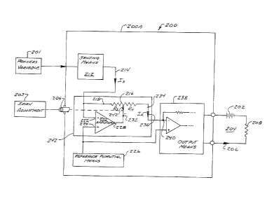
In FIG. 3, a transmitter 200 made according
to this invention senses a process variable 201 such as
~3~17~
temperature, pressure, or flow in a process plant. The
transmitter 200 is a loop-power transmitter which is
energized by a power source 202 in the 4-20 mA
industrial process control loop 204. The amplitude of
a 4-20 mA current 206 flowing in the loop is con~rolled
by transmitter 200 according ~o the sensed process
variable. A resistance 208 is included in loop 204 and
is represen~ative of a device for receiving the 4-20 mA
signal such as a meter, loop amplifier, or recorder.
The transmitter 200, power source 202, and resistance
; 208 are coupled together in a series circuit.
Transmitter 200 is sealed in a closed housin~ 200A to
protect the electronic components from damage by the
harsh process control environment. The transmitter
span adjustment 203 is coupled through a drive coupling
205 sealed in the transmitter's housing so that
adjustment can be ma~e without opening the housing.
A sensing means 212 comprises a sensor and
associated circuitry ~or providing a sense current 214
proportional to the sensed process variable. The
sensing means 212 senses the process variable over a
wide range of input spans, for example, a 12:1 range of
spans. ~ potentiometer 21~ receives the sense current
214 at a first terminal 218. An operational amplifier
220 has an inverting input 222 coupled to first
terminal 218 for sensing a potential at terminal 218.
The input 222 is a high impedance input so that
substantially all of sense current 214 flows into first
terminal 218 of the potentiometer. A non-inverting
input 224 of the amplifier 220 is coupled to a
reference potential 226 in the transmitter. ~n output
228 of amplifier ?20 is coupled to wiper terminal 232
~l3~J7~
of potentiometer 216. ~ span-adjusted current 236
flows out of terminal 234 of potentiome~er 216 and into
a summing junction 240 of an output means 238. The
summing junction 240 is held at substantially the same
potential as input 224 by feedback within output means
238. Potentiometer 216 presents a variable impedance
~3 between terminals 218 and 232; potentiometer 216
presents a variable impedance R4 between terminals 232
and 234; and potentiometer 2:L6 presents a substantially
fixed resistance IR3 ~ R4) between terminals 218 and
234. The potentiometer 216 thus comprises a first
impedence means having a first impedence ~4 coupled
between the output of amplifier 22~ and the output
means 238. The potentiometer 216 further comprises a
second impedance means having second impedance R3
coupled between output 228 and input 222.
The resistance R3 is in a feedback loop
between the output 228 and the input 222 of amplifier
220. ~esistance R3 controls the ratio of signal
voltage at output 228 to sense current 214. The
resistance R4 controls the ratio of span-adjusted
current 236 to the signal voltage at the output 228.
Adjustment of the span adjustment potentiometer 216
therefore adjusts these two ratios simultaneously and
provides a desired relationship between the gain and
the resolution factor of the transmitter, as explained
: below. The amplifier 220 and the potentiometer 216
comprise span-controlling means 2~2 which receiYes the
sensed current 214 and provides a span-adjusted current
236. The gain of the span-controlling means 242 is the
ratiO (delta Ia/delta ~s) which is controlled by the
potentiometer adjustment substantially according to the
` formula:
-` ~L3n~7940
Gain = delta Ia = R3 Eq. 3
_ .
dPlta Is R4
The span of transmitter 200 is a ratio o a change of
output current to a change of input pressure. In thi~
transmitter it is desirable to adjust the span so that
the transmitter is adaptable to a wide range of input
pressures to utilize the wide range of the input
sensor. For example, when the transmitter 200 is used
in one application, i~ may be desirable to have a 16 mA
change in output curre~t represent a 2 psi input
pressure change but when the same transmitter 200 is
used in another applica~ion, it must be adjusted BO
that a 16 milliampere change in ou~put current
represents a 100 psi input pressure change. In this
lS transmitter 200 it is desirable to adjust (calibrate)
the transmitter's span with a high degree of resolution
over a wide range of span settings. In the transmitter
depicted in FIG. 3 the output resolution (delta Is/Is)
of the span-controlling means 242 is found to be:
delta Is = delta R . ~2 + R3 + R4~ Eq. 4
Is R3 + R4 ~ R4 R3 ¦
The output resolution of ~he span-controlling means 242
is equal to the potentiometer resolution (delta R/(R3 +
R4~) multiplied times a resolution factor ~2 + (R3/R4
2s + ~R4/R3)). Both the gain of the circuit and the
resolution factor of the circuit are controlled by the
adjustment of the potentiometer 216. The resolution
factor of the circuit as a function of the gain of the
circuit is depicted graphically by curve 102 in FIG. 2.
By way of an example, if a potentiometer is used that
has a resolution ~R/~R3 ~ R4) equal to 0.02~ and the
output resolution of the transmitter must be less than
.: :
. ~ . ' '
, i:
,.
`" ~307~40
--10--
or equal to 0.2% to provide accurate calibration adjustment
of the span, then the potentiometer will provide tha_ much
output resolution (0.2%) where the resolution factor is less
than or equal to 10 as determined from Eq. 4. Referring now
to FIG. 2 it can be seen that for a resolution factor of 10
or less the gain can be adjusted from a maximum of 10 to a
minimum of 0.2. The turndown ratio of the transmitter 200 is
therefore the ratio of the upper gain setting to the lowest
gain setting or 50:1. As can be seen from the curve 102, the
resolution factor is a nonlinear function of the gain. The
span-controlling means 242 provides a wide range of
adjustment of the span of the transmitter without excessive
limitation on the turndown ratio of the transmitter. The
high turndown ratio permits use of the wide span range of
span of the sensing means 212.
In FIG. 4, a schematic diagram of a transmitter 300
which capacitively senses a differential pressure is shown. A
differential pressure sensing means 302 includes a capacitive
differential pressure sensor 304. Pressure sensor 304 may be
constructed as shown in my issued U.S. Patent number
3,793,885, for example, to provide a pair of çapacitances Cl
and C2 which vary according to the differential pressure P
applied to sensor 304. A voltage-controlled oscillator (VC0)
306 is an integrated circuit VC0 such as Motorola TM type
MC14046 TM and provides excitation on conductor 308 which is
coupled to the moving plate 310 of sensor 302 through fixed
capacitor 312. Diodes 314 and 316 couple currents from the
fixed capacitor plates of sensor 302
~3(~79~
-11-
to control circuit 318. Control circuit 318 senses the
currents from diodes 314 and 316 and provides an output
Vc on conductor 322 represen~ative of these currents.
The output Vc on conductor 322 is coupled to
VCo 306 to control the frequency of the VCO's
excitation signal on conductor 308. A thermistor 324
in the control circuit 318 is a means for stabilizing
the operation of transmitter 300 over a desired range
of operating temperatures. Fixed capacitor 326, diodes
328 and 330 and potentiometer 332 are coupled together
to form a linearity adjustment circuit and
potentiometer 332 is adjusted to provide a more linear
relationship between the sensed pressure and the
excitation freguency. The VCO 306, sensor 3~4, diodes
31~ and 316, the linearity adjustment circuit and the
control circuit 318 are coupled together in a closed-
loop fashion as shown in FIG. 4 to provide an
excitation signal on conductor 308 with a substantially
fixed amplitude and a frequency representative of the
applied pressure P. Diodes 334 and 336 are coupled
from the sensor 304 to a conductor 338 and provide a
sense current Is representative of the sensed pressure
P.
The sense current Is is coupled via conductor
338 to a span-controlling circuit 340. In circuit 340,
the current Is is received at a summing junction 342.
The summing junction also receives a current from
terminal 344 of span adjustment potentiometer 346 and a
current coupled from a zero adjustment circuit
comprising fixed resistor 348 and zero adjustment
potentiometer 350 as shown in FIG. 4. An amplifier
352A has an inverting input 354 coupled to ~he summing
.
. . ~
!,
.~ .
~3~79~0
-~2-
junction 342 for sensing the potential at the summing
junction. The input 354 of amplifier 352 is a high
impedance input and substantially all of the current
from the zeroing network plus the cusrent Is from the
; 5 sensing means flows into terminal 344 of the span
adjustment potentiometer 346. An adjustable contact
356 of potentiometer 346 is coupled to the output of
amplifier 352A. A non-inverting input of amplifier
352A is coupled to a *l volt reference potential in the
transmitter. A bypass capacitor 358 is coupled between
the inverting input 354 and the non-inverting input 360
to minimize the effects of noise and provide a smooth
output from the transmitter. A terminal 362 of the
span adjusting potentiometer 346 supplies an adjusted
output current Ia to the output means 364. The span
adjustment potentiometer 3~6 and the zero adjustment
potentiometer 350 each have sealed adjustment screws
347, 351 that are accessible from the ou~side of a
housing 353 around the transmitter, permitting
adjustment of the span and zero of the transmitter
without removing a cover on the transmitter.
Operation of span-controlling circuit 340 is
similar to the operation of span adjustment circuit 242
of FIG. 2 and Eq. 3 and Eq. 4 above also apply to the
span adjustment circuit 340. Resistance R3 of
potentiometer 346 is connected in a feedback loop
around amplifier 352 to control gain. Resistance R4 of
potentiometer 346 is in a feed-forward circuit between
wiper 356 and output means 364 to control current Ia.
Resistance R3 and R4 vary oppositely as potentiometer
346 is adjusted. When R3 in~rreases, R4 decreases and
vice versa. The arrangement with oppositely varying
~3~794(~
resistances controlled by a span adjustment, one in a
feedback loop and one in a feed-forward path provides
the desired high turndown ratio.
The output means 364 receives the span-
adjusted current Ia and provides a 4-20 mA output
current at terminals 366 and 368. The amplitude of the
output current is controlled by the span-adjusted
current Ia. The transmitter is powered by the 4-20 mA
current loop and output means 364 also includes supply
means for energizing the transmitter 300 from the loop.
Loop current flows into the transmitter circuitry
through rectifier 370 which provides protection against
reverse polarity currents. Transistor 372 ~ontrols ;
loop current in response to a signal applied by
amplifier 374A. Amplifier 374A senses a po~ential at
summing junction 376. Span-adjusted current Ia and a
current If represe~tative of loop current flow into
summing junction 376. A factory-trimmable resistance
378 also provides a substantially f ixed current It into
the summing junction 376. The resistance of resistor
378 is factory-trimmed to reduce interaction between
; the span-adjustment and the zero adjustment. Reference
diode 374C and amplifier 374B comprise supply means and
provide a regulated potential designated as "+6V
SOURCE" in FIG. ~ which is coupled to ~ransmit~er
circuitry at points designated "~6V~, such coupling not
being shown in FIG. 4 to provide clarity. A resistive
divider network 382 is connected to the +6V SOURCE and
provides other regulated potentials to the transmitter
circuitry. Bypass capacitors 384 are coupled to
divider network 382 to reduce noise levels in the
divider network 382. A +lV SOURCE potential is
13~79~
-14-
generated by the divider and is coupled to transmitter
circuitry at points designated "+lV". A buffer
amplifier 352B receives a potlential from the divider
network 382 and provides a regulated potential "+2V
SOURCE" which is routed to points in the transmitter's
circuitry designated "~2V".
Amplifiers 352A, 352B, 352C and-352D are
portions of a quad amplifier integrated circuit such as
a type LM246 made by National Semiconductor.
Amplifiers 374A and 374B and reference diode 374C are
portions of a type LMl0 integrated circuit made by
National Semiconductor.
- The transmitter's circuitry is enclosed in a
sealed housing 353 and connections are made to the
transmitter at terminals 366 and 368 without opening
the electronics housing. Zero adjustment 386 and span
adjustment 388 are received at sealed adjustment screws
347 and 351 without opening the housing. The
transmit~er 300 may thus be installed and also adjusted
in a hostile process control atmosphere without
exposing the circuitry to the environment.
While the invention has been described in
terms of a poten~iometer control of the span-
adjustment, it will be understood by those skilled in
the art that other impedance means with limited
resolution, such as D/A converters, or switching
circuits may also be used within the scope of this
invention.