Note: Descriptions are shown in the official language in which they were submitted.
~30~34B~
P 38 18 843.0
Method of and Circuit Arrangement for
Recovering a 8it Clock from a Received
Digital Communication Signal
The present invention relates to a method of and a circuit
arrangement for recovering a bit clock from a received
digital communication signal wherein a clock generator
at the rece;ving end generates a reference clock whose
frequency is N times the frequency of the bit clock
wherein a counter operating as a frequency d;v;der and
having at least N count states ;s cyclically incremented
by the reference clock so as to divide the reference
clock to the frequency of the bit clock which is de-
livered at one of its outputs~ wherein the period of
the bit clock is divided into N equal portions of time
and wherein the effective pulse edge of the b;t clock
provided at the output of the counter occurs at the count
determined by N/2.
Such a prior art circuit arrangement (DE-AS 24 35 687)
contains a clock generator a counter and a logic
circuit. The frequency of the clock generator-is n times
the frequency of the received bit clock and the counter
is controlled by the logic circuit and synchronously
with the pulses from the clock generator in such a way
14LAKnr/~e/19o89 D. Pauer 1
3~ :
8~L8
-- 2 --
as to be incremented either not at all or by one or two
counts depending on the deviation from the desired posi-
tion. In the synchronous case, an effective pulseedge of
the bit clock occurs at the center of each bit unit of
the received signal.
Such prior art circuits generate a bit-clock signal whose
phase is derived from the beginning, i.e., a leading edge,
of a received pulse of the communication signal. Because
of the commonly used transmission codes (e.g., HDB3, AMI)
and the nonideal character;stics of the transmission
lines, the duration of the received pulses may d;ffer
from the desired ualue.
This means that the leading edge of the received pulse
of a bit sequence occurs earlier or later, which in-
evitably leads to continuous phase corrections that
counteract a freguency drift for a short time and may
thus lead to a higher bit-error rate.
It is the object of the invention to provide a method
and a circuit arrangement whereby a phase-locked bit
clock can be recovered from a rece;ved digital communi-
cation signal, so that even if pulses with different
durations are received, the effective pulse edge of the local
bit clock will lie as close in time to the center of the
actually receiued pulse as possible.
According to the invention, this object is attained by the
D. Pauer 1
~3~8448
72430-90
method of recovering a bit clock signal from pulses of a digital
communication signal received at a receiving end of a transmission
path, said method comprising the steps: generating a reference
clock at the receiving end whose frequency is N times a nominal
frequency of the bit cloclc, using the reference clock to
cyclically increment a counter having at least N count states so
as to divide the reference clock down to the frequency of the bit
clock, such that an output of the counter provides an effective
pulse edge of the bit clock signal at count state N/2, using a
phase evaluation logic circuit to determine a first count state of
said counter at which a leading edge and a second count state of
said coun~er at which a trailing edge of each received pulse of
the communication signal respectively occur, determining a
respective center count state of said counter corresponding to
each said received pulse, said center count state being equal to
the average of said first and second count states, and for ~aid
each received pulse, delivering a phase correction signal to the
counter only if the thus determined center count state is not
equal to said count state N/2.
According to another aspect, the invention provides
apparatus for recovering a bit clock signal from pulses of a
digital communication signal and for correcting the phase of the
recovered clock if the received pulses are not symmetrically
disposed about the effective pulse edye of the recovered clock,
said apparatus comprising: a clock generator circuit; a phase
evaluation logic circuit for determining whether the received
pulses are symmetrically disposed about the effective pulse edge
~Q8~4~
72430-90
of the recovered bit clock, and if not so symmetrically disposed,
for outputting first or second correction signals indicating that
the center of the received pulse leads or lags the recovered bit
clock respectively; a counter operating as a frequency divider and
having at least N count states, a clock input connacted to the
clock generator, a first correction input for causing the counter
to assume more than N coun~ states, a second correction input for
causing the counter to assume less than N count states, and a
plurality of counter outputs representative of the counter's
current count state and coupled to a respective plurality of
inputs of the phase evaluation logic, the most significant bit of
said counter outputs representing the effective pulse edge of the
recovered clock; a two-s~age serial-parallel shift register having
a clock input connected to the clock generator, a serial input
coupled to a receive line, and two parallel outputs coupled to two
respective further inputs of the phase evaluation logic; first
latch means coupled between said phase evaluation logic circuit
and said first correction input for temporarily storing said first
corrections signal output by the phase evaluation logic; and
second latch means coupled between said phase evaluation logic
circuit and said second correction input for temporarily storing
said second correction signal output by the phase evaluation
logic.
Since, according to the invention, the time positions,
i.e., the counts for the leading edge and the trailing edge of a
received pulse are determined, the actual duration of the received
pulse can be ascertained. This makes it possible to distinguish
3~
c f~
~ 3C9844L8
72430-90
between a genuine phase shift and an only momentary edge drift due
to pulse durations which are shorter or longer than the desired
duration. If, for example, the duration of a pulse is too long
and the effective pulse edge of the bit clock occurring at the
count N/2 nevertheless lies at the center of the received pulse,
this indicates a momentary edge drift, but, according to the
invention, no phase correction will take place.
Further advantageous features of the subject matter of
the invention are set forth in the subclaims.
An embodiment of the invention will now be explained
with reference to the accompanying drawings, in which:
Fig. 1 is a block diagram of a circuit arrangement in
accordance with the invention;
Fig. 2 is a first timing diagram serving to explain the
method in accordance with the invention;
- 3B
~3~8~48
-- 4 --
Fig. 3 is a second timing diagram serving to explain
the method in accordance with the invention,
and
Fig. 4 is a truth table for the phase evaluation
logic in accordance w;th the invention.
First, the circuit arrangement according to the invention
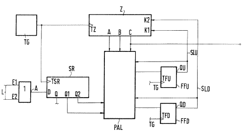
wiLl be described with the aid of Fig. 1.
The circuit includes a clock generator TG, which generates
a reference clock whose frequency ;s N times the fre-
quency of the received clock. In the example being de-
scribed, the frequency of the reference clock is
16.384 MHz, and the factor N is 8, so that the fre-
quency of the bit clock is 2.048 MHz. The clock generator
TG can be implemented with a convent;onal TTL crystal
oscillator.
The clock generator TG is connected to a clock input
TZ of a counter Z having at least N count states, here
8 count states. Accordingly, the counter has three out-
puts A, B, C, which are connected to a phase evaluation
logic PAL, with a frequency of 2.048 MHz, which is equal
to the frequency of the bit clock, being obtainable from
the output C.
Also connected to the phase evaluation logic PAL is a
receive line L, over which the digital communication
signal to be received is transmitted.
D~ Pauer 1
~3Q~ 8
It will be assumed that the signal is transmitted in
the HDB3 code. The incoming positive pulses are applied
to a first input E1 of a logic OR gate OR, and the in-
coming negative pulses to a second input E2. An output
A of the OR gate OR is connected to a signal input D
of a serial-parallel shift register SR.
A clock input TSR of the shift register SR is connected
to the clock generator TG. A first output Q1 and a sec-
ond output Q2 of the shift register SR are connected to
thephase evaluation logic PAL.
Because of the received asynchronous communication signal
applied to the signal input D of the shift register SR,
it may happen that the setup and hold t;mes commonly re-
quired for such logic elements cannot be met, so that
short-time undefined states may occur at the output Q
of the first stage of the shift register SR. To avoid
such errors, use is made of a three-stage shift register
SR in which the output Q of the first stage is not wired.
Thus, the first output Q1 and the second output Q2, which
are connected to the phase evaluation logic PAL, re-
present the outputs of the second and th;rd shift-register
stages, respectively (cf. Fig. 4).
The phase evaluation logic PAL is connected to a first
flip-flop FFU for temporarily storing a correction signal
for inserting an additional count pulse, henceforth desig-
nated UP, and to a second flip-flop FFD for temporarily
~. Pauer 1
~3Q84~8
storing a correction signal for suppressing a count
pulse from the counter, henceforth designated DOWM.
The two flip-flops are designed here as D flip-flops,
with a signal output QU of the first flip-flop FFU con-
nected by a flrst control line SLU to a first correction
input K1 of the counter Z, and a signal output QD of the
second flip-flop FFD connected by a second control line
SLD to a second correction input Q2 of the counter Z.
In addition, the two signal outputs QU, QD are fed back
to the phase evaluation logic PAL.
The method according to the invention will now be explained
with reference to the timing diagrams of Figs. 2 and 3
in connection w;th the c;rcu;t arrangement of F;g. 1.
In F;g. 2, line a shows the waveform of the 16.384-MHz
reference clock generated by the clock generator TG. Line
b shows the waveform of the reference c~ock div;ded by
a factor of N=8 by the counter Z, i.e~, the bit clock
w;th a frequency of 2.048 MHz. Since the counter Z has
N=8 count states, which appear at its three outputs A, B,
C, cf. Fig. 1 (three outputs = 23 = 8 count states), the
period T of the bit clock, as shown in line c of Fig. 2,
is divided into N=8 equal portions of time which re-
present the 8 count states.
A pulse sequence incoming on the receive line L is first
applied to the signal input D of the shift register SR.
Line d of Fig. 2 shows a received pulse, and lines e
and f show the pulses at the first output Q1 and the
D. Pauer 1
13~844~
second output Q2, respectively, which were delayed by
the shift register SR.
The bit combinations at the two outputs Q1, Q2 of the
shift register SR, which is clocked by the reference
clock, are as follows:
Q1 Q2
O O = no pulse
1 0 = leading edge of the pulse
0 1 = trailing edge of the pulse
1 1 = pulse present
In the absence of a pulse, cf. lines e and f and count
1 or 2 in line c, the two outputs Q1, Q2 of the
shift register SR will provide a logic O to the phase
evaluation logic PAL. If the leading edge of a pulse
arrives, the output Q1 will be a logic 1 and the output
Q2 a logic 0. As long as the received pulse is being
shifted through the shift register, the two outputs Q1,
Q2 are at logic 1 (data pulse present). A tra;ling pulse
edge, cf. lines e and f and count O or 1 in line c, then
signifies that the output Q2 (line f) is still at logic
1 while the output Q1 has already changed to logic 0.
These four different bit combinations are continuously
communicated to the phase evaluation logic PAL at the
pulse repetition rate of the reference clock.
From the counts made available via the three outputs A,
B, C of the coun~er Z, cf. line c, and the bit combina~ions
D. Pauer 1
13al8~
-- 8 --
transferred synchronously therewith via the two outputs
Q1, Q2 of the shift register SR, the phase evaluation
logic PAL determines the counts at which the leading
edge and the trailing edge of each received pulse of
the communication signal occur.
In Fig. 3, line a shows the counts of the counter Z tsee
3lso Fig. 2, l;ne c)~ wh;ch divide the period T of the
bit clock, line b in Fig. 3, into 8 equal portions of
time.
The effective pulse edge of the local bit clock,
F;g~ 3, l;ne b~ is located at the count determined by
a N/2=4 (so-called center-of-bit sampling); this is
illustrated by the solid vertical line in Fig. 3.
The phase evaluat;on logic PAL sends a correction sig-
nal to the counter Z over the first or second control
l;ne SLU, SLD only if, irrespective of the duration of
a received pulse, the pulse edge of the local bit
clock is not located at the center of the received pulse
of the communication signal (will be explained ;n detail
below).
In the following, different cases characterizing the
;nvention will be disclosed with the aid of the truth
table for the phase evaluation logic shown in Fig. 4.
The two-part truth table shows in the first line of the
u~per half the 8 counts applied to the phase evaluation
logic PAL via the three outputs A, B, C. The second line
D. Pauer 1
~1 3~8~4~8
shows the bit combination 10 (leading pulse edge) at the
two outputs Q1, Q2 of the shift register SR at the re-
spective counts shifted by two counts with respec-t to
line a. In the third line~ designated FFU, a O or 1 has been
entered if at the counts entered in line two~an evaluation
"leading pulse edge" represents no received Dulse or a
leading received pulse, respectively. Similarly, a O or 1 has
been entered in the fourth line, designated FFD, if at the
counts entered in line two~an evaluation "leading pulse edge"
represents no received pulse or a
lagging received pulse, respectively.
The upper half of the truth table thus gives an evaluation
of the criterion "count at a leading edge of the received
pulse in relation to the count for the effective pulse
edge of the bit clock, characterized by N/2=4".
It is assumed, for example, cf. Fig. 3, line c, that
a leading edge of a received pulse is determined at a
count of 1, cF. Fig. 4, line a. Assuming that a pulse to
be received has a desired duration of T/2, the puLse
edge detected at count 1 occurs one count too early in
relation to the count N/2=4, hereinafter referred to as
"sampling count". As a result, a correction signal DOWN
is stored in the second flip-flop FFD (cf. Fig. 4,
fourth line, entry "1"). If the trailing edge of a re-
ceived pulse, cf. Fig. 3, line c, and Fig. 4, lower half
of the table, second line Q1=0, Q2=1, is determined at
count 7, cf. Fig. 4, lower half, first line, the received
pulse is a pulse whose duration differs from the desired
duration T/2 (by 2 counts), but which is symmetrical with
D. Pauer 1
~3Q~34~8
- 10 -
respect to the sampling count. However, s;nce this ex-
tended pulse is sampled at the center with respect to
the sampling count, according to the invention, no
correction signal is required, so that the correction
signal DOWN stored in the second flip-flop FFD is re-
~set, cf. Fig. 4, lower half of the table, fourth line,
entry 1. The entry 1 in the truth table signifies that
a previously stored correction signal DOWN ~or UP) is
reset.
If the leading edge of a received pulse occurs at count
3, cf. Fig. 3, line f, and Fig. 4, upper half, first line,
and the associated trail;ng pulse edge at count 5, cf.
Fig. 4, lower half, first line, the received pulse is a
pulse whose duration is shorter than the desired
duration T/2, but which is aga;n symmetrical with re-
spect to the sampl;ng count N~2. In response to the
leading pulse edge at count 3, a correction signal UP
;s stored in the first flip-flop FFU, cf. Fig. 4, upper
half, entry 1 in the third line. As the phase evaluation
logic PAL has determined that the pulse is "only" a
shortened but correctly sampled pulse, the correction
signal UP stored in the first flip-flop FFU is reset,
cf. Fig. 4, lower half, third line, entry 1 below count
5 of the first line.
In the two previously described cases, cf. Fig. 3, lines
c and f,according to the invention, no phase corrections
are performed since the actual duration of the received
pulse can be derived from the determination of the leading
D. Pauer 1
~3~844~3
- 11 -
and trailing pulse edges, and since no corrections
are necessary for pulses that are symme.rical with re-
spect to the sampling count.
If the leading pulse edge occurs at count 1~ cf. Fig. 3,
line d, and Fig. 4, upper half, first and fourth lines,
and the trailing pulse edge at count 5, this indicates an
actual phase shift (lagging) since the pulse is unsymmetrical
with respect to the sampling count 4.
As can be seen in Fig. 4, upper half, fourth line, a
correction signal DOWN is stored in the second flip-flop
FFD and sent over the second control line SLD to the
second correction input K2 of the counter Z (cf. FigO 4,
Lower half, fourth line, entry X=don't care, ;.e.,
no reset). The correction signal DOWN causes a count
pulse of the counter Z to be suppressed.
If the leading pulse edge occurs at count 3 and the
trailing pulse edge at count 7, cf~ Fig~ 3, line e~ and
Fig. 4, first and third lines, this indicates an actual phase
shift (leading). A correction is now performed by
storing a correction signal UP in the first flip-flop
FFU. The correction signal UP is applied over the first
control line SLU to the first correction input K1 of
the counter Z and causes an additional count pulse to
be inserted.
The entire circuit arrangement according to the invention
can be implemented with a crystal oscillator for the
clock generator TG and a programmable logic array. It
thus takes up only little space, is inexpensive, and re-
quires no discrete components.
D. Pauer 1