Note: Descriptions are shown in the official language in which they were submitted.
~3~
TECHNICAL FIELD
The present invention relates to a high
resolution dot generator system for use in color
scanners and, more specifically, to a dot generator
system including a light emitting diode ("LED") array
and a system for controlling the array.
BACKGROUND AND OBJECT5 OF THE INVENTION
Multiple color printing processes require
production of color halftone separations which are
used to make printing plates corresponding to each
color ink to be printed. In a traditional four color
printing process it is necessary to produce cyan,
magenta, yellow and black halftone separations which
are used to make corresponding printing plates for
printing cyan, magenta, yellow and black process inks.
Originally, halftone separations were made
on a camera by projecting an image of the original
artwork through a color filter and a halftone screen
of the desired pitch and angle onto photosensitive
film. The camera procedure required substantial
training with various techniques and was tedious and
error prone. With the advent of electronic imaging,
camera halftone techniques gave way to electronic
color scanners. In an electronic color scanner the
original artwork is scanned, typically in a line by
line and pixel by pixel fashion, and an
electronically controlled beam of light exposes a
simulated halftone separation onto photosensitive
film. Electronic color correction, unsharp masking
and under color removal are commonly provided and, of
course, the effects of halftone screens must be
electronically reproduced.
To be competitive, modern color scanners
must provide high resolution halftone images. In
.
~3~
practice, this is accomplished by exposing a number
of high resolution "microdots" or "dotels" to produce
each halftone dot. Modern high quality scanners
commonly use laser-based dot generators to produce
khe requisite high resolution microdots, e.g. in
excess of 2,500 microdots per inch. Lasers have been
~ound satisfactory since many types of lasers operate
in the blue and green regions of the spectrum, which
is appropriate for exposing orthochromatic film, and
lasers can be controlled to produce concentrated,
high intensity beams of light.
Lasers, however, are costly and difficult to
incorporate into a scanning dot generator. Moreover,
it has been found that lasers can produce only a
limited, small number of exposure beams. Thus, high
quality contemporary scanners incorporating laser dot
generators are very expensive and, as a praçtical
matter, are limited to approximately 8 to 10 exposure
beams.
Lower resolution scanning printheads, such
as for low cost phototypesetting and scanning, have
used LED's to expose photosensitive materials. See
U.S. Patent 4,378,149 issued to Ebner entitled "High
Speed, Low-Cost Character Printerl', U.S. Patent
4,342,504 issued to Ebner entitled "LE~-Fiber Optic
Character Printer", U.S. Patent 3,952,311 issued to
Lapeyre entitled "Electro-Optical Printing System'i,
U.S. Patent 4,096,486 issued to Pfeifer entitled
"Recorder", U.S. Patent 4,107,687 issued to Pfeifer
entitled "Recording Device" and U.S. Patent,
3,850,517 issued to Stephany entitled "High Speed
Printout System". More recently, monolithic LED
arrays have been produced. See U.S. Patent 4,73~,714
issued to Takasu entitled "Optical Print Head With
LED Diode Array", and U.S. Patent 4,644,342 issued to
~3~ t
Abbas entitled "Array Of Light Emitting Diodes For
Producing Grav Scale Light Images". U.K. Patent
Application 2,099,221 entitled "Light Emitting Diode
Array Devices and Image Transfer Systems", and
; s published December l, 1982, discloses one or two row
monolithic LED arrays having up to 1000 light
' emitting areas per inch.
r Notwithstanding the foregoing disclosures,
no suitable LED dot generator source capable of
10 producing microdots at the high resolution and
intensity required for high quality color scanning is
known. Indeed, only U.S. Patent 4,365,275 issued to
Berman entitled "Method for Producing Images on
Radiation Sensitive Recording Mediums" makes any
15 attempt to use an LED source in a color scanner. Yet
Berman resorts to conducting light from individual
LED sources through optical fibers to a matrix array
which is optically reduced in an exposing head.
; Although Berman claims to obtain 22,500 dot areas per
20 square inch, the system there disclosed is not known
; to have found substantial commercial acceptance.
To the contrary, to date the color scanner
industry has not adopted any LED source as yielding
acceptable color scanning separations. Rather, the
25 numerous drawbacks of heretofore known LED sources,
including fàbrication difficulties, inconsistent
light output, and fewer types of photosensitive
material responsive to the red light customarily
; produced by LED's, have led to the general perception
in the color scanner industry that LED devices are
inappropriate for use as a light source in high
quality color scanner dot generators. Improvements
have been made in photosensitive materials responsive
to red light, but to date no reliable hiyh
3s resolution, high intensity LED source has been
proposed for use in a color scanner.
t
: A
,~
~3~
v In addition, it has long been Xnown that the
effects of a halftone screen may be electronically
simulated by storing a "dot density profile" of a
halftone dot, recalling individual microdot density
values from the dot density profile using
trigonometrically rotated address values, and
superimposing the microdot density value onto a
picture signal to determine whether a microdot
exposure is to be made. See Landsman U.S. Patent
3,961,~32. It is also known that trigonometric
address rotation may be performed by successively
incrementing the address values. See Gall U.S.
Patent 4,499,489. Rosenfeld U.S. Patents 4,350,996
and 4,456,924 also relate to addressing a stored dot
density profile using trigonometrically transformed
addresses. However, the foregoing systems for
electronically generating halftone screens generally
relate to laser beam exposure devices and, more
particularly, to systems in which a single dot
generator controls but a single laser exposure beam.
For example, Gall discloses an address sequencing
system for controlling a single laser beam which
makes a scanning ex~osure in the scan line direction
around the circumference of a rotating drum.
Although Gall suggests that multiple exposure beams
could be provided, including multiple beams created
by a line of LED's, Gall teaches that a plurality of
screen generators are necessary for such a multiple
beam system ~see Gall col. 12, lines 28-31).
Therefore, it is one object of the present
invention to provide a relatively low cost halftone
dot generator capable of producing high resolution
microdots on a photosensitive surface.
A further object of the present invention is
to provide a halftone dot generator including an LED
~3~36~6
- 6 -
source capable of producing high resolution microdot
images on a photosensitive material.
Another object of the present invention is
to provide a compact and lightweight LED array
appropriate for use as the exposure source in a dot
generator system for a high quality color scanner.
It is yet a further object of the present
invention to provide an LED array dot generator
system for creating multiple microdot exposure beams.
Another object of the present invention is
to provide a dot generator system and method for
controlling activation of an LED array to create
multiple exposure beams for exposing a screened
halftone image onto photosensitive film.
It is yet a further object of the present
invention to provide a dot generator system and
method capable of controlling multiple LED exposure
beams with a single dot yenerator.
These and other highly desirable and unusual
results are accomplished by the present invention in
an economical, lightweight and compact LED dot
generator system appropriate for use in a a color
scanner to produce high resolution separation images.
Objects and advantages of the invention are
set forth herein and in part will be obvious
herefrom, or may be learned by practice with the
invention, the same being realized and attained by
means of instrumentalities and combinations pointed
out in the appended claims.
The invention consists of the novel parts,
constructions, arrangements, combinations, steps and
improvements herein shown and described.
SUMMARY OF T~E INVENTION
In accordance with the present invention,
~3~ ~
-- 7
there is provided a multiple beam halftone dot
generator system including an LED array with
staggered rows of LED ' s . Advantageously, one dot
. generator is used to control activation of the LED's
; s on the LED array to produce a multiple beam microdot
exposure.
In accordance with a particular embodiment
of the invention there is provided a dot generator
system for a color scanner including means for
l 10 providing a picture value for use in exposing a
halftone separation comprising:
; an LED microchip array having multiple
staggered rows of LED ' s, said LED microchip array
: being mounted opposite to and imaged upon the
15 exposure surface of a color scanner, said LED
microchip array being movable in a two dimensional
. . coordinate system relative to said exposure surface;
. an addressable stored dot density profile
; array, said dot density profile array having a
zo micxodot density value stored at each memory
address;
bit slice means for determining a dot
density profile array address value and recalling
the corresponding microdot density value;
.: 25 compare logic means for comparing said
recalled micxodot density value with a picture value
to determine whether an LED on said LED array will
be activatecl, said compare logic means transmitting
an exposure clata bit indi.cating whether the
corresponding LED is to be activated;
serial to parallel converter means for
receiving said exposure data bits from said compare
logic means and accumulating said bits to construct
an exposure data word equal in length to the numb.er
3s of active LED's on said LED array,
t
: ~,
~3~
- 7a -
stagger compensation logic means for
receiving said exposure data word from said serial
to parallel converter means, said staggex
compensation means introducing delay timing to data
. s bits corresponding to at least some of said
staggered LED rows, said delay timing being equal to
the time required for said LED microchip array to
traverse the distance on said exposure surface
between each staggered row and the first rowj
output buffer means for receiving a
modified exposure data word from said stagger
compensation means and transmitting said modified
exposure data word to said LED array; and
clock generator means for providing a
timing reference for said delay timing and
transmittal of said modified exposure data word from
said output buffer to said LED array, said clock
generator means also providing a stroke pulse to
said LED array and a picture value request pulse for
2D signaling the color scanner that the dot generator
system is ready to receive the next picture value.
From a different aspect, and in accordance
with a particular embodiment of the invention, there
is providad a method of generating halftone
25 separation images in a color scanner including means
. for providing picture values, the method comprising:
providing an LED microchip array having
multiple staggered rows of LED's;
mounting said LED microchip array opposite
30 and movable in two dimensions relative to an
exposure surface;
projecting an image of said LED micxochip
array onto said exposure surface;
providing an addressable dot density
. 3s profile array, said addressable dot density profile
:
. .
.' t
~"
~3~
- 7b -
array storing a microdot density value at each
memory address;
addressing said addressable dot density
profile array with a dot density profile array
s address to retrieve a microdot density value;
comparing said microdot density value with
a picture value to produce an exposure data bit
indicating whether a corresponding LED on said LED
microchip axray is to be activated;
applying microdot, flyback and scanline
increment values to said dot density pro~ile array
address to advance to the next microdot density
value corresponding to the next microdot to be
exposed onto a photosensitive sheet disposed on sai
exposure surface in a microdot line by microdot line
and scanline by scanline scanning exposure;
accumulating a number of said exposure
data bits equal to tha number of active LED ' S on
said LED microchip array to produce an exposure data
word;
mod:ifying said exposure data word to
compensate for the staggered configuration of said
i LED microchip array;
activating said LED microchip array in
25 response to said modi~ied exposure data word.
The preferred LED microchip array has four
staggered rows of six LED ' S in each row. The LED ' S
are formed in a known manner in a substrate which
.
acts as a common connection. A first insulation
30 layer is deposited over the substrate surrounding
the LED wells and individual electrodes, one sur-
rounding and contacting each LED well, are led in a
unique pattern to the periphery of the monolithlc
chip for contact with the LED array drive circuitry.
3s Briefly c~tated, the electrode~ for the LED ' ~ of the
top and bottom rows are led upward and downward,
.
~;.,a~
- 7c -
respectively, to contact points disposed on the top
and bottom chip edges, whereas the contact
electrodes for three LED's in each of the middle
rows are led to each side of the chip for contact.
5 This unique electrode pattern, together with the
configuration of the staggered array, advantageously
obtain high intensity exposures for high resolution
microdots with effective thermal dissipation. A
second insulation layer is disposed over the
electrode layer. In order to prevent undesirable
light variations caused by light from the LED's
escaping through the substrate to the sides of the
LED's, a metalised masking layer is disposed over
the entire array. The second insulation layer
electrically isolates the metalised masking layer
from the electrodes.
In practice, the lightweight and compact
LED microchip array is mounted with associated
optics on a transport carriage opposite the exposure
, 20 surface of
. ~
:~3lP~
a color separation scanner. Preferably, the LED
microchip array is mounted opposite the surface of a
rotating exposure drum and is selectively activated
in accordance with the preferred dot generator system
to obtain microdot resolutions in excess of 2,800
dots per inch. Further in accordance with the
invention, the dot generator advantageously includes
a single dot generator system connected to the LED
chip array for controlling activation of all LED's.
The scanner also includes an original artwork input
scanner for scanning original artwork to generate
picture pixel values for each color separation.
In accordance with the dot generator system
and method of the present invention for controlling
the LED array, a scanned picture value for a given
color separation is compared to a microdot density
value recalled from a halftone dot density profile
array ("DDPA") addressably stored in random access
memory ("RAM"), and a determination is made whether a
corresponding microdot is to be exposed by activating
an LED on the LED array. Bit slices are provided for
incrementing the x and y DDPA address parameters and
maintaining a running total of the DDPA address
during ongoing scanning. Advantageously, the bit
slices may simply be 32 bit adders with on board
memor~ capable of storing microdot line increment
values, flyback increment values, scanline increment
values and a running address total for each halftone
separation. During exposure scanning of a
separation, the bit slices sequentially increment the
running total DDPA address across the microdot line
to be produced in order to recall from the DDPA the
microdot density value corresponding to each microdot
in a microdot line perpendicular to the direction of
rotation of the exposure drum, i.e. the axial
.
~3~6~
9 _
direction, up to the number of active LED's on the
LED array. Each microdot density value recalled from
the DDPA is compared to a picture value to determine
whether each active LED in the array is to be turned
on to expose a microdot on the microdot line. After
sequencing the DDPA address across a microdot line,
the bit slices increment the running total DDPA
address with a "flyback" increment in order to reach
the DDPA address corresponding to the first microdot
of the next microdot line to be exposed on the
exposure drum. Address incrementing continues in
this manner microdot by microdot and microdot line by
microdot line until the end of a scanline exposure in
the circumferential direction around the drum, at
which time the bit slices increment the starting DDPA
address by a "scanline" increment value to reach the
DDPA address corresponding to the first microdot of
the first microdot line of the next scanline in the
axial drum direction. DDPA addressing continues in
this manner incrementing microdot by microdot,
microdot line by microdot line, and scanline by
scanline until a given separation scan is completQ.
Advantageously, overflow of the running total DDPA
address may be ignored since the DDPA is symetrical
and the remaining portion of the address effectively
corresponds to the address within the next symetrical
; halftone dot to be produced.
A compare logic compares each microdot
density value recalled from the DDPA with a corrected
picture value from the scanned original artwork to
determine whether an LED is to be activated to expose
a corresponding microdot on the halftone separation.
Preferably, negative microdot density values are
stored in the DDPA, with the compare logic adding the
negative microdot density value to the positive
~3~
1~
picture value and looking at the sum to determine
whether the corresponding LED is to be activated.
The compare logic outputs a single data bit
indicating whether an exposure is to occur at a given
microdot, i.e. whether the corresponding LED is to be
activated. A serial to parallel converter
accumulates exposure data from the compare logic and
constructs a word equal in length to the number of
LED's in use on the LED array and, hence, equal to
the number of microdots on a single microdot exposure
line on the rotating exposure drum.
Because the LED array does not consist of a
single line of LED's, a stagger compensation logic is
provided to coordinate activation of each LED in the
staggered LED rows in order to expose a single,
aligned microdot line from one word of microdot
exposure data received from the serial to parallel
converter. The stagger compensation logic transmits
the exposure data bits corresponding to the first row
of LED's without delay to an output buffer connected
to the array. However, exposure data bits
corresponding to the second and subsequent staggered
LED rows are delayed from being transmitted to the
output buffer and LED array for a period of time
corresponding to the time required for the exposure
drum to rotate until each staggexed row is aligned
with the point on the drum surface where the first
row of LED's were activated in response to
corresponding exposure data. Advantageously, the
output buffer and LED may receive bits of data for
each LED row corresponding to different microdot
lines, so that each row of the LED array exposes a
different portion of different microdot lines during
a single stroke pulse.
A clock generator controls the time delay
introduced by the stagger compensation logic,
transmittal of exposure data from the output buffer
to the LED array, activation of the LED array with a
stroXe pulse, and transmission of a signal to the
picture value source to obtain a new picture value.
A bit slice control monitors the output buffer to
coordinate addressing of the DDPA RAM and comparison
of microdot density values to picture values with
availability of the serial to parallel converter.
That is, transmittal of an exposure data word the
output buffer to the LED array also triggers
transmittal of a word from the stagger compensation
logic to the output buffer and from the serial to
parallel converter to the stagger compensation
logic. Thus, transmittal of data from the output
buffer to the LED array is indicative of availability
of the serial to parallel converter to receive new
data from the compare logic.
The LED dot generator system in accordance
with the present invention advantageously provides a
low cost multiple beam LED exposure source capable of
providing high resolution hal~tone separation
exposures. Advantageously, the unique configuration
of the highly compact LED array obtains high
intensity exposure from each LED with effective
thermal dissipation. Remarkably, in the LED dot
generator syskem operated in accordance with the
present invention the multiple beam LED array is
controlled with a single electronic dot generator,
thereby further reducing the cost and complexity of
the dot generator. Significantly, the LED dot
generator system in accordance with the invention
obviates the need for expensive, bulky and complex
laser sources traditionally used in high quality
color separation scanners.
_ 12-
It will be understood that the foregoing
general description and the following detailed
description as well are exemplary and explanatory of
the invention but are not restrictive thereof.
BRIEF DESCRIPTION OF THE DRAWINGS
The accompanying drawings, referred to
herein and constituting a part hereof, illustrate
preferred embodiments of the present invention, and
together with the description serve to explain the
principles of the invention, in which:
FIG. 1 is a top plan view of the preferred
LED array in accordance with the dot generator system
of the present invention;
FIG. 2 is a top plan view of the LED array
shown in FIG. 1 without the mask and second
insulation layers;
FIG. 3 is a partial cross-sectional view of
one of the LED's shown in FIG. 1, taken along line
3-3 of FIG. 1;
FIG. 4 is a perspective view of one LED;
FIG. 5 is an elevation view of the preferred
~ LED array mounted opposite the surface of a rotating
: exposure drum and imaged thereon by a lens;
FIG. 6 is a block diagram of the dot
generator system for controlling the preferred LED
array;
FIG. 7 is a diagramatic illustration of a
stored dot density profile array;
FIG. 8 is a block diagram illustration of
one embodiment of a stagger compensation logic in
accordance with the dot generator system of the
present invention.
- 13-
DETAILED DESCRIPTION OF_THE PREFERRED EMBODIMENTS
In accordance with the present invention an
LED dot generator system is provided including an LED
microchip array controlled by a single dot generator
to produce mul$iple exposure beams.
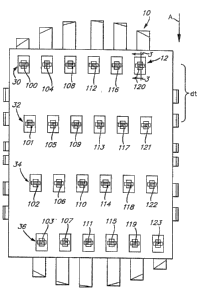
Figure 1 is a top plan view of the preferred
arrangement of tha LED microchip array 10 utilized in
the present dot generator system. The preferred LED
array 10 has four staggered rows of six LED's, with
each LED measuring approximately five by eight
microns and spaced apart on center from the LED's of
the same row by approximately thirty six microns.
The scanline direction of motion of the exposure
surface relative to the array is indicated by arrow
A. Figure 2, a top plan view of the preferred LED
array without mask or second insulation layers, shows
the preferred LED electrode configuration which
obtains heretofore unknown thermal dissipation
efficiency and compact spacing of the very small
LED's. Figure 3 is a partial cross-sectional view of
a single LED 12 taken along line 3-3 of Figure 1, and
Figure 4 is a perspective view of an LED 12. Figure
5 is an elevation view of the preferred scanner
configuration wherein the LED array is mounted
opposite from and imaged onto the surface of a
rotating exposure drum. Figure 6 is a block diagram
of the dot generator control system for controlling
activation of the LED array. Figure 7 is an
illustration of a stored dot density profile array,
and Figure 8 is a block diagram illustration of a
stagger compensation logic useful in the present dot
generation system.
Referring more specifically to Figures 3 and
4, the construction of an individual LED 12 is
shown. A substrate 14 of an "N" type material in
- ~3~
- 1~
c~ntact with a common 16 is doped with a light
emitting "P" type impurity to ~orm a light emitting P
type rectangular "well" region 18 within the
substrate. A first insulating layer 20 is deposited
over the N type surface surrounding the P type well
region 18. Insulating layer 20 has a rectangular
opening of a size no larger than each P type well
region 18, thereby insuring that no part of the N
type substrate 14 is exposed.
An electrode 22 is deposited above first
insulating layer 20 surrounding rectangular well
region 18. Electrode 22 extends into well region 18
and contacts the P type material contained therein.
Preferably, èlectrode 22 contacts the P-type well at
at least two points on opposite sides of the well
region. It is important that effective electrical
contact be established between the electrode 22 and
the P type material in well region 18. Other than
the electrode to well region contact points,
electrodes 22 are electrically isolated from
substrate 14 by insulation layer 20. A second
insulating layer 24 is deposited atop the electrodes
22. Rectangular openings are formed in the second
insulating layer surrounding and exposing each
rectangular well 18. Second insulating layer 24
covers substantially all of electrode 22,
specifically including the outer perimeter of the
electrode region surrounding well region 18.
A metalised masking layer 26 is deposited
above second insulating layer 24. Masking layer 26
is sufficiently opaque to block stray light generated
in well region 18, i.e. the LED, passing out to the
side through substrate 14. The mask is electrically
isolated from the electrode by second insulation
layer 22, and has a rectangular opening surrounding
.~ 3~;P~6~
the opening in the second insulating layer.
Preferablys the openiny in the masking layer is
smal~er tha~ the outer perimeter of electrode 22 to
ensure effective masking. ~he masking layer and, to
some extent, the electrode, ensure that light
generated within LED well region 18 directed
transversely through the substrate is not visible
from above the array. In this marmer, stray light is
suppressed and only light from well defined LED's is
visible from above the array. Those skilled in the
art of fabricating LED microchips will be familiar
with techniques for fabricating the LED array of the
present invention in accordance with the foregoing
description.
As shown in the perspective view of Figure
4, LED well region 18 is visible from above the
array, surrounded by the first insulation layer 20,
electrode 22, second insulation layer 24 and mask
layer 26. When the LED well region is excited by
passing current from electrode 22 through well region
18 and substrate 14 to common 16, the LED well 18
emits high intensity light visible from above the
array, with masking layer 26 obscuring any stray
light transmitted outward through the substrat~ to
the sides of the well region.
As shown in Figures 1 and 2, a staggered
array of LED's formed in accordance with the
foregoing description provides a high resolution LED
array for use in the dot generator system according
to the present invention to expose high quality color
separations. The preferred LED array consists of
four evenly spaced parallel rows 30, 32, 34, 36, each
containing six LED's. Thus, the overall shape of the
array is that of a parallelogram. The exposed
light-emitting well region of each LED measures about
. .
~3~ 6
_ 1~
eight microns long by five microns wide, and the
center to center spacing between LED's of any given
row is approximately thirty six microns. Preferably,
all rows are equally spaced s~ that the center to
center distance between LED's in adjacent rows is
about so micxons.
In Figure 2, the LED array of Figure 1 is
illustrated without the metalised masking layer or
the second insulation layers in order to show the
unique electrode pattern of the preferred LED array.
As shown, the electrode leads 37 for LED's 100, 104,
108, 112, 116, 120 of the first, top row 30 are led
upward to electrical contacts 38 on the top edge of
the microchip array. In the second row 32,
electrodes 40, 42 corresponding to LED's 101, 121
lead directly out to each side of the array to
contacts 41, 43, respectively. Electrodes 48, 50
corresponding to center LED's 109, 113 lead up and
outward between the first and second rows to contacts
49, 51 on each side of the array. Electrodes 56, 58
corresponding to intermediate LED's 105, 117 lead
down and outward between the second and third rows
32, 34, respectively, to contacts 57, 59 on each side
of the array.
Similarly, in the third row 34 electrodes
64, 66 corresponding to LED's 102, 122 lead directly
out to contacts 65, 67 on each side of the array.
Electrodes 72, 74 corresponding to intermediate LED's
106, 118 lead upward and outward to contacts 73, 75
on each side of the array, and electrodes 80, 82
; 30 corresponding to center LED's 110, 114 lead downward
and outward to contacts 81, %3. Finally, electrode
leads 88 for the LED's 103, 107, 111, 115, 119, 123
of the fourth, bottom row 36 lead downward to
contacts 89 disposed along the bottom ed~e of the
.
~3~
chip.
It has been found that the array geometry
described above is particularly well-adapted for use
in combination with the dot generating exposure
system according to the present invention to expose
halftone separation images onto a sheet of
photosensitive material mounted on the surface of
rotating exposure drum 126 opposite the LED array,
with the LED array being movable parallel to the
rotating drum surface (see Fig. 5). Advantageously,
the staggered array can provide up to twenty four
exposure beams, unlike traditional laser-based
systems which typically provide only eight to ten
beams, all of which are ~ontrolled by a single dot
generator system. Of course, different combinations
of LED's and LED rows can be activated to obtain
different numbers and configurations of beams. It is
also contemplated that the LED array may be movably
mounted opposite other types of exposure surfaces
such as a flat surface, within the scope of the
present invention. Hereinafter, the dot generator
system will be discussed in the context of the
preferred twenty four element, four by six row LED
array mounted opposite a rotating exposure drum. As
used herein, the term "active" LED means an LED
activated for use during exposure, and it will be
appreciated that reference to active LED's may refer
to less than all LED's on the array activated for use.
The stagger geometry is quite precise, and
permits accurate control over microdot size and shape
without altering fundamental microdot resolution.
The pitch between adjacent scan lines is determined
by such factors as required output speed and picture
resolution. However, with the present invention a
coarse or fine pitch may be obtained at constant
_ ~8-
speed by selectively activating all LED's or a
subcombination of a lesser number of LED's. The
fundamental resolu~ion of each LED remains unchanged,
which is advantageous where, for example, text and
graphics are to be exposed at different resolutions
during the same scan. This cannot be done with a
laser dot generator having a limited number of
exposure beams. There, the scanning speed and/or the
fundamental resolution of each beam must be altered
to change the scan line pitch.
The preferred array geometry provides
distinct advantages in a dot generating exposure
system for a drum-type color separation scanner.
First, the LED's are sufficiently small to expose
fine microdots acceptable for high-resolution color
separation scanning, e.g. in excess of 2,gOO
microdots per inch. Finer resolution may be obtained
using relatively simple optical reduction. Second,
the preferred geometry permits high power, on the
order of lO milliamps, to be supplied to and drive
each LED at high current density to obtain an intense
exposure source. Third, the four by six staggered
array allows the excitation of the LED's to be timed
during scanning in accordance with the system of the
present invention to expose a continuous microdot
line of up to twenty four immediately ad~acent
microdots. That is, the dot generator control system
described below controls activation of each staggered
row to permit displacement of the exposure scanning
drum surface relative to the array in an amount equal
to the distance between rows, i.e. about 9O microns,
before activating the next row with corresponding
exposure data.
Thus, the dot generator system of the
present invention including an LED array with
36~
19-
staggered rows and corresponding dot generator
control system obviates the need for one or two rows
of small, closely spaced LED's which would be subject
to thermal and electrical .interference between
electrodes and/or LED's. Indeed, even if a linear
array of twenty four LED's measuring five by eight
microns could be constructed, the LED's and electrode
leads would necessarily be spaced close together,
resulting in thermal and/or electrical interference.
As shown in Figure 5, the LED array 10 is
mounted opposite the surface of a rotating exposure
drum in a color scanner. More specifically, LED
array 10 is mounted on a substrate 124 with
appropriate interconnections and an image of the
array is focused by a lens 128 onto the film bearing
surface of rotating exposure drum 126.
As described more fully below, in the dot
generator system and method of the present invention,
activation of the LED's in rows 30, 32, 34, 36 is
controlled so that each row is imaged at
substantially the same location on the rotating
exposure drum to expose a single row of up to twenty
four microdots.
Figure 6 illustrates in block diagram form
the preferred dot generator system 130 for
controlling LED array 10. Dot generator system 130
includes a dot density profile array random access
memory ("DDPA RAM") 132 which stores addressable
microdot density values, a microprocessor 134 for
creating incremental address values for each color
separation and furnishing the incremental address
values to bit slices 136 via VME bus 138 and bit
slice control 140. As explained more fully below,
the incremental address values take into account the
screen parameters, i.e. screen pitch and angle, to be
,P~
_ 20-
v superimposed on each halftone, and corresponds to the
line by line activation sequence of the LED array. A
compare logic 142 receives ~icrodot density values
from the DDPA R~M as accessed by bit slices 136, and
compares each microdot density value to picture data
received from a data buffer 144. The picture data
corresponds to one pixel of a color. Based upon the
comparison of the microdot density value with the
picture pixel value, the compare logic determines
whether each individual LED will be turned "ON" to
expose a microdot on the halftone film. The compare
logic supplies an exposure indication bi~ for each
microdot of information to a serial to parallel
converter 146, which accumulates the exposure
indications into a word equal in bit length to the
number of "active" LED's on the LED array 10~ That
is, although the preferred LED array contains twenty
four LED's it is contemplated that it may be
: desirable to use less than all LED's of the array,
; the remaining LED/s being "inactive".
The parallel exposure data word from the
serial to parallel converter is furnished to a
stagger compensation logic 148 which introduces
appropriate time delays which take into account the
staggered row construction of the LED array and the
rotating speed of the ~xposure drum to ensure that
each row of LED's is activated at substantially the
same point on the surface of drum 126, thereby
exposing a single line of microdots on the halftone
film in response to one exposure data word from the
serial to parallel converter. The time delayed
exposure signals are sent by stagger compensation 148
to an output buffer 150 and on to LED array 10. A
clock generator 152 monitors the timing of data
~ transfer from output buffer 150 to array 10, triggers
: 35
,
~3~
- 21-
a stroke pulse to activate the LED array, and
transmits a signal indicating when the system is
ready for the next pixel of picture data to be loaded
into input data buffer 144. Of course, output
linearization may be applied in a known manner where
appropriate, such as by including one or more output
linearization look up tables applied to one or more
signals in the system, e.g. the output signal of data
buffer 144.
In the preferred embodiment of the invention
the DDPA RAM is a 128 x 128 program logic array
stored in static ram which stores 12 bit density
values corresponding to each microdot. By way of
example, Figure 7 illustrates an example of a square
dot density profile 154 stored in DDPA RAM. As
shown, the halftone dot uses an x, y coordinate
system with the common zero 156 at the center of the
array. By way of illustration, zero density values
occur at the center of the dot profile 156, with
maximum density values "D" occurring at each extreme
corner 158 of the dot profile. For this example of a
square halftone dot, fifty percen (50%) density
values lie along diamond 160. Of cour.se, other
halftone dot configurations and stored density values
having other than 12 bits of data may be suitable.
For reasons which will ~ecome apparent, negative
microdot density values are preferably stored in DDPA
RAM 132.
It has advantageously been found that all
addressing of DDPA RAM for a given halftone
separation may be performed by continuous adding of
incremental address values in a predetermined
sequence. Thus, the bit slices assume all LED's of
the array are arranged in a single row, i.e. as in
the case of a single row of microdots exposed by a
- 22-
linear array. Under these circumstances, the
following illustration depicts the relationship of
eac~ m?crodot line and scanline relative to the axis
and circumference of the rotating drum.
axis
circumference
Q ~ Scanline l Scanline 2
microdot line 1 1 2 3 4...... N 1 2 3 4..... N... to end
of scan
microdot line 2 l 2 3 4...... N l 2 3 4..... N
microdot line 3 1 2 3 4........... N 1 2 3 4..... N
.
.
to end of scanline
As shown, each microdot line extends axially
across the drum surface up to N microdots, which
corresponds to the number of active LED's in array
lO. The number of microdot lines extends to the end
of the scanline in the circumferential direction and
the number of scanlines extends to the end of the
scan.
Advantageously, it has been found that
incrementing the start DDPA RAM address across each
microdot of a microdot line within one scan,
introducing a flyback to reach the first microdot of
the next microdot line of the same scanline, and
introducing a scanline advance increment to the start
DDPA address, in that order, provides simple,
~3/~
- 23-
v accurate and fast addressing of DDPA RAM 132
throughout any given scan. In ac~ordance with the
preferred methQd, microprocessor 134 calculates the
microdot, flyback and scanline incremental address
values for each halftone color separation and
transmits these incremental values to the bit slices
136 prior to commencing exposure scanning. Of
course, by simple trigonometry it is possible to
incorporate the desired screen parameters, e.g.
screen pitch and angle, for each separatlon into the
corresponding incremental address values, so that
DDPA address incrementing incorporates the selected
screen angle. The microdot line incremental address
values dx, dy corresponding to the distance between
each microdot of a microdot line may be expressed and5 calculated as follows:
dx = (Spi x Cos A)
~Lpi x N)
dy = (Spi x Sin A~
(Lpi x N)
Similarly, the address increment
corresponding to the flyback distance between the
last microdot of one microdot line and the first
microdot of the next microdot line in the same
scanline may be expressed and calculated as follows:
fx = (Spi x Cos A~ - (N-l)dx
Dpi
fy = (Spi x Cos A) - (N-l)dy
Dpi
-,
3L3~
_ 24-
Finally, the scanline increment value
corresponding to the distance from the first microdot
of the first microdot line of one scanline to the
first microdot of the first microdot line of the next
scanline may be expressed and calculated as follows:
lx = (Spi x Cos A)
Lpi
ly = (Spi x Sin A)
Lpi .
where:
Spi = reguired halftone screen period in
number per inch
Lpi = number of scanlines per inch on output
N = number of microdot beams across one
microdot line; also equal to the
number of active LED's on the array
Dpi = number of microdot elements per inch
in circumferential drum direction
A = required screen angle
Advantageously, microprocessor 134
calculates the incremental values dx, dy, fx, fy, lx,
ly for each color separation and transmits these
incremental address values to bit slices 136 in
advance of scanning. Thus, prior to scanning
exposure bit slices 136 has in memory all incremental
address parameters for each halftone separation, and
DDPA RAM 132 contains addressable microdot density
~3~ 6
_ 2
values.
~ t the beginning of each scanning exposure,
bit slices 136 start at address X = O, Y = o. During
sequential addressing steps, bit slices 136 add
incremental values dx, dy to determine the address
seguence for scanning across a row of microdots.
These values are added (N-l) times, with bit slices
136 thereafter adding the row flyback values fx, fy
to commence scanning the addresses for next microdot
line in the same scanline. DDPA RAM addresses are
sequentially determined for each microdot in each
microdot line within one scanline until the end of
the scanline. Thereafter, bit slices 136 add
scanline incremental values lx, ly to the start DDPA
address corresponding to the first microdot of the
first microdot line in any given scanline in order to
increment to the DDPA RAM address corresponding to
the first microdot of the first microdot line of the
next scanline. Sequential addressing for each
microdot line of each scanline continues in this
manner until the end of a separation scan.
In the preferred embodiment wherein bit
slices 136 each comprise a 32 bit adder with onboard
memory, 32 bit adding is performed to calculate each
incremental memory address. Typically, however, the
address word length for DDPA RAM 142 is much
shorter. For example, the DDPA RAM address word
length might be 12 bits. To conform the incremented
address value to the DDPA address length, only the
most significant digits of the incremented address
value are used to indicate the next address value.
However, all 32 bits continue to be included in
subsequent incremental additions for accuracy.
Moreover, since the dot density profile array is
symetrical and repetitive, any overflow bits are
~3~ 6~
_ 2~
ignored since this merely indicates that the
incremental address values have entered the next
halftone d~t of the electronic screen.
The compare logic 142 preferably comprises
an adder or subtracter and a comparator to determine
whether the sum or difference is greater or less than
zero. Preferably, the compare logic is a 12 bit
digital comparator including an adder which receives
a negative microdot density value from DDPA RAM 132
and a positive picture value from buffer 144 and adds
the two together. Where the sum of the picture and
microdot density values is greater than or equal to
zero, i.e. the picture value is greater than the
recalled microdot density value, the compare logic
determines that an LED is to be activated
corresponding to expose the corresponding microdot.
Where, however, the sum is negative, i.e. the picture
value is less than the recalled microdot d2nsity
value, the compare logic determines that no exposure
is to be made for the corresponding microdot. For
each LED corresponding to one microdot, compare logic
142 transmits a single bit of data indicating whether
the LED is to be turned "ON".
One or more serial to parallel converters
146 convert the single bits of exposure data received
from compare logic 142 into a single exposure data
word corresponding in length to the number of active
LED's on array 10. By way of example, serial to
parallel converter 146 would accumulate and transmit
an 8 bit exposure data word if 8 LED's are activated
for use on array 10, or a 12 bit data word if 12
LED's are activated for use on array lO.
Referring again to Fig. 3, serial to
parallel converter 146 is also connected directly to
data buffer 144. Preferably, the picture value
~3~ 6~
- 27_
received by and stored in buffer 144 also contains
two bits of data indicating whether or not any
picture is to be exposed and, if not, whether the
corresponding picture area is to be completely
exposed or left blank. This data is monitored by
serial to parallel converter 146 and, where no
picture is to be exposed, the output data from the
serial to paralle]. converter may be "forced". That
is, the exposure data word transmitted by serial to
parallel converter 146 ~orces all active LED's on
array lO to turn on or off, as required. This is a
convenient feature of the present invention since it
permits, for example, a border area to be completely
exposed or left blank. Advantageously, exposure of
picture data may be resumed immediately after the
border or other "forced" area is complete.
Up to this point the present dot generator
system has been discussed as if the exposure data
word transmitted by serial to parallel converter 146
corresponded directly to and would be us~d to
activate a single line of LED's to expose a straight
line of microdots. The preferred LED array, however,
consists of several staggered rows of LED's.
Consequently, the exposure data word must be
transformed to conform to the array configuration.
This requires that transmittal of the exposure data
bits corresponding to each staggered LED row be timed
to cause excitatio-n of each staggered row in response
to corresponding exposure data to occur at the same
position on the rotating drum surface. In short,
activation of the LED's must be timed so that the
~irst row is turned on at one point on the exposure
drum, with each subsequent staggered row being turned
on in response to corresponding exposure data at the
same point on the rotating drum.
36~
- 28_
To accomplish this result, stagger
compensation logic 148 introduces an appropriate time
delay before transmitting corresponding exposure data
to the second and subsequent staggered rows of LED's
to the LED array.
Referring to Figure 1, the first bit of
exposure data received from serial to parallel
converter 66 corresponds to LED 100. The second bit
corresponds to LED 101, the third bit to LED 102, and
so on through as many LED's are active and to be
controlled. With regard to a single exposure word
received from the serial to parallel converter,
stagger compensation logic 148 immediately transmits
exposure data bits corresponding to the first row of
LED's 30 to output buffer 150 and on to array 10
; 15 without delay. However, the stagger compensation
; logic delays transmitting the exposure data bits
corresponding to the second row of ~ED's 32 for a
period of time dt, where dt equals the length of time
required for the rotating exposure drum to rotate
until the second row of LED's is aligned with the
point on the drum surface where the first row of
LED's w~s activated with corresponding undelayed
data. Similar but longer time delays are introduced
before transmitting corresponding exposure data bits
to the third and fourth staggered rows. Of course,
where the stayger distance between the rows of LED's
is constant, and the exposure drum rotates at
constant speed, the time delay for data corresponding
to the third LED row will be 2dt and the time delay
for data corresponding to $he fourth row will be 3dt.
By way of example only, where the twelve
LED's corresponding to reference numerals 100 through
lll on Fig. l are active and are to be controlled to
expose a microdot line, the stagger compensation
_ 29-
logic transmits the first, fifth and ninth exposure
data bits of an exposure data word directly to output
buffer 150 without delay. The second, sixth and
tenth exposure data bits are delayed for a period of
time dt before being transmitted to output buffer
150. The third, seventh and eleventh data bits are
delayed for a period of time 2dt before being
transmitted to output buffer 150 and the fourth,
eighth and twelfth data bits are delayed a period of
time 3dt before being transmitted to output bufEer
150.
It is contemplated that stagger compensation
logic 148 may consist of a set of first in first out
("FIF0") registers corresponding to the rows of LED's
for which data is to be delayed. This embodiment is
illustrated in Figure 8, which illustrates 12 bits of
data received from serial to parallel converter 66.
Stagger compensation logic 148 transmits the first,
fifth and ninth bits directly to output buffer 150.
The second, sixth and tenth bits are stored in FIF0 A
and are transmitted to output buffer 150 after a
period of time dt. The third, seventh and eleventh
bits are stored in FIF0 B and are transmitted to
output buffer 150 after a period of time 2dt.
Similarly, the fourth, eighth and twelfth bits are
stored in FIF0 C and are transmitted to output buffer
150 after a period of time 3dt.
In an alternative embodiment of stagger
compensation logic 1~8, the first, fifth and ninth
bits are transmitted without delay to output buffer
150 and the entire exposure data word received from
the serial to parallel converter is stored in
addressable memory. After a number of clock cycles
corresponding to dt, the second, sixth and tenth bits
are read from memory and transmitted to output buffer
3~3~ i6
_ 30-
v 150. After a further number of clock cycles
corresponding to the peri~d of time 2dt, the third,
seventh and eleventh bits of data are read out of
memory and transmitted to output buffer 150.
Finally, after a number of clock cycles corresponding
5 to the period of time 3dt the fourth, eighth and
eleventh bits are read from memory and transmitted to
output buf fer 150.
As will readily be appreciated from the
foregoing discussion, the stagger compensation logic
constructs and transmits to output buffer 150 an LED
array exposure command word quite different from the
exposure data word received from the serial to
parallel converter. Thus, during ongoing scanning
the stagger compensation circuit receives an exposure
data word corresponding to the exposure data for one
microdot line exposure on the drum surface. The
stagger compensation logic transmits a modified
exposure data word consisting of undelayed exposure
data for the first LED row and delayed exposure data
for the second, third and fourth LED rows, as to
which first row exposures have previously been
completed. Thus, during ongoing scanning, the LED
array simultaneously exposas four different portions
of four different microdot rows on the photosensitive
material.
Output buffer 150 receives the modified
exposure data word from stagger compensation logic
148 and, in response to a clock pulse from clock
generator 152, transmits the modified exposure
command data to LED array 10.
Clock generator 152 i5 connected to stagger
compensation logic 148, output buffer 150, LED array
10 and to the source of the picture value data.
Thus, the clock generator controls the timing of
u transmittal of data from output buffer 150 to array
~0 and provides a stroke pulse directly to the array
to trigger the array in response to the modified
exposure data received from output buffer 150. The
clock also controls the timing sequence of the
stagger compensation logic and each transmittal of a
new exposure command word from the stagger
compensation logic to output buffer 150. Finally,
the clock generator sends a pulse to the picture data
source each time the dot generator system is ready
for a new picture value to be loaded into data buffer
144. Of course, since the size of one microdot is
much smaller than one scanned pixel of picture data,
the same picture value stored in buffer 144 is
compared multiple times with microdot density values
recalled rom DDPA RAM 132. Consequently, the clock
generator signal to the picture data source is sent
after a predetermined number of comparisons have been
performed using one picture value.
As shown in Figure 6, bit slice control 140
monitors output buffer 150 so that addressing of the
DDPA RAM is consistent with the timing of output
buffer 150. Because transmittal of exposurP command
data from output buffer 150 is determinative of the
transmittal of data from stagger compensation 148 to
output buffer 150 and, hence, from serial to parallel
converter 146 to stagger compensation 148, the timing
of data transmitted by output buffer 150 is also
indicative of the availability of serial to parallel
converter to receive new exposure bits from compare
logic 142. Therefore, monitoring of the output
buffer by the bit slice control is indicative of the
appropriate timing for bit slices 136 to perorm .
additional DDPA R~M addressing and density value
comparisons in order to replenish serial to parallel
6~
_ 32-
converter 146.
~ inally, i~ is also contemplated that one or
more output lineari~a~i~n look up tables may be
necessary to ens~re ~ linear response of the digital
dot generating sys~ y way of example, such a
linearization look up table might be connected to the
picture data buffer and/or to the output buffer to
ensure a linear exposure signal.
In operation, DDPA RAM 132 is addressably
loaded at start up by microprocessor 134, via VME bus
138, bit slice control 140 and hit slices 136 with
negative microdot density values corresponding to the
desired halftone d~t pr~file. Prior to commencement
of scanning, the ~icroprocessor calculates the
microdot line incremental address values dx, dy, the
microdot line flyback incremental address values fx,
fy, and the scanline advance incremental address
values lx, ly and transmits these values to ~e stored
by x and y bit slices 136.
During scanning, bit slices 136 under the
direction of bit slice control 140, increment the
DDPA RAM address ~crDs~ a microdot line by
successively adding dx, dy to the initial start
addrèss. After completing a microdot line, i.e. by
conducting N-1 additions of dx, dy to reach the end
of the LED array, the bit slices increment the DDPA
~AM address by fx, fy in order to flyback to the
first microdot of the next row in the same scanline.
After completion of on~ scanline, bit slices 136 add
lx, ly to the DDPA star* address to increment the
DDPA RAM address to ~he first microdot of the first
microdot line of the next scanline. Incremental
addressing continues in this manner until the end of
a halftone exposure scan. Advantageously, since
incremental address values and separate running
~.3~.P~6~;
- 33-
v addresses for all four halftone separations are
stored in bit slices 136, the dot generator system
can readily alternate between halftone exposures
during exposure drum rotation to produce multiple
separations on one piece of film. Alternatively,
upon completion of one halftone separation exposure
the bit slices are capable of immediately commencing
the next halftone exposure without any need to have
the microprocessor recalculate and load incremental
address values.
Compare logic 142 compares microdot density
values received from DDPA RAM 132 with a picture
value received from data buffer 144, preferably by
adding the negative microdot density value to the
positive picture value and looking at the resulting
sum. The compare logic transmits a single bit of on
or off data corresponding to one microdot and, hence,
one LED to serial to parallel converter 146. The
serial to parallel converter accumulates bits of
exposure data from the compare logic and builds an
exposure data word corresponding in length to the
number of active LED's on the LED array and, hence,
to the number of microdots to be exposed during a
single exposure stroke. Stagger compensation 148
receives the exposure data word from serial to
parallel converter 146 and introduces appropriate
time delays to bits corresponding to LED's in the
second and subsequent staggered LED rows. The
stagger compensation transmits to outpllt buffer 150 a
modified exposure word containing exposure data for
up to four portions of different microdot lines to be
exposed by the LED array. Clock generator 152
provides a time reference for the delays introduced
by stagger compensation 148 and controls the timing
of transmittal of exposure data from output buffer
~3~36~
- 34_
150 to array 10, activation of the LED array, and
transmittal of a request from dot generator system
130 to the picture value source to obtain the next
pixel picture value to be processed and exposed. Bit
slice control 140 monitors the output of output
buffer 150 in order to coordinate the timing of
address sequencing by bit slices 130 and comparisons
of microdot density values in order to replenish the
serial to parallel converter.
Although particular illustrative embodiments
of the present invention have been described herein,
the present invention is not so limited. Various
changes, substitutions and modifications may be made
thereto by those skilled in the art without departing
from the spirit or scope of the invention, as defined
in the appended claims. By way of example only, it
may be possible to construct and utilize in
accordance with the present invention an LED
microchip array having greater or less than twenty
four LED's arranged in various configurations of
staggered rows other than the preferred four by six
staggered row array. It will also be appreciated
that terms used in the foregoing disclosure,
specifically including but not limited to "light",
"top", "bottom", "center", "intermediate", "active"
and "inactive" are used for convenience in describing
the invention and are not restrictive thereof.