Note: Descriptions are shown in the official language in which they were submitted.
ODS-lll.l I 3 0 8 7 ~ 8
VOICE AND IMAGE TELEBONFE~ENCINf~ SYSTEM
INCLUUING PAP~RLESS FACSIMILE ~EANS
f~IELD ~F THE INVENTI~N
The present invention relates generally to
electronically operated image data input and display
systems, as paperless telefacsimile rneans, and more
particularly to display communications systems having
o integrated image data input means and visual display
means to provide paperless telefacsimile capability in
combination with voice capability. The imaye data
input means is adapted to transmit image data to both
the integral display and a remote location, while the
display is adapted to receive input from both the
integral image input means and remote means. The
electronic data input means is touch sensitive image
data input means capable of simultaneously ana
accurately digitizizing information as that
information is entered upon an electrically conductive
surface thereof. Such information is electronically
displayed and is also transmitted downstream for
storage, display, reproduction and/or information
processing.
BACKGROUN~ Of THE IhVENTIOW
Electronic teleconferencing is an economical
way of bringing people together for conferences and
30 meetings, without the costs, dislocations, delays and
inconveniences associated with travel. In electronic
teleconferencing, conferants sit in their own
conference rooms and offices, and confer by conference
call methodology. Typically, teleconferencing is
supported by hard telefacsimile capability. However,
teleconferencing systems, to be fully practical, must
q~
1 3087q8
ODS-lll.l
,~
be capable of two way visual data communications.
This requires digitizing visual information input and
converting digital ~ata to visual data, i.e.,
digitizing and displaying data as in a paperless
telefacsimile. Recently electronic data transmission
devices capable of digitizing and reproducing visual
information manually entered upon a surface, e.g., an
electrically communicative surface, have been
developed and introduced. These devicés constituted
an independent parallel means of supporting
teleconferencing.
The previous data transmission devices
adapted for digitizing and reproducing information
manually entered on a surface fall generally into one
of two categories: digitizing tablet systems and
electronic copyboards. Both of these devices possess
significant technological limitations for two-way
electronic data communications. Electronic copyboards
lack the means, structurally and functionally, for
reproducing incoming data from a remote location.
Oigitizing tablets, alone, are incapable of receiving
and displaying data from a remote data input source.
Teleconferencing requires the use of one line
for voice communications, one line for hand copy
facsimile, and one line for data communications.
Moreover, no means is provided for interaction between
the lines.
BRIEf SUMMARY OF THE INVENT~ON
The shortcomings of the prior art are
obviated by a telephone touch pad for electronic data
image communications having, in combination, a touch
sensitive position sensor for totally solid state
image data entry, a display system in combination
therewith and capable of being updated thereby and by
i30~
UDS-lll.l
--3--
external data inputs or data signal processing means,
an electronic connection to both, the associated
display system and a remote display system so as to
provide paperless telefacsimile means, and
interconnection, in the case of a system adapted for
use with an analog network, means for
telecommunication through the analog data
communications system. Generally, the analog network
will be carrying data signals at frequencies within
lo the acoustical or audible bandwidth from about 300 Hz
to 3,400 Hz.
The present invention utilizes an integratea
solid state touch sensitive position sensor and a
solid state display which synergistically interact
with each other. The integrated system is not only
capable of simultaneously aisplaying information
entered thereupon, but is also capable of encoding and
transmitting that information as well as receiving
like information, all in a very accurate manner
thereby functioning as a loczl electronic memo pad and
as a paperless telefacsimile means. Therefore, the
touch position sensor, display, and associated
communications capability of the present invention
avoids the limitations inherent in previous electronic
teleconferencing and data communication systems and
thus, represents a significant advance in the fiel~ of
integrated electronic data input, display, and
communication systems.
The data teleconferencing system of the
30 present invention, which we also refer to herein as a
teléphone memo pad, includes a paperless telefacsimile
means comprising data input and display means. The
data input and display means comprises a solid state
touch sensitive position sensor having suitable drive
means, a solid state display having suitable drive
means, first data bus means to allow display of the
1 30~7~
ODS-lll.l
-4-
touch position sensor input on both the related solid
state display and a remote display, and second data
bus means to allow display of data, from a remote data
input on the solid state display.
While the data teleconferencing system may be
used with either digital or analog telecommunication
network means, and, when used with digital
telecommunications network means, with either serial
or parallel data, the initial commercial use will most
o likely be with serial analog data over analog
telecommunication means operating acoustical
frequencies (300 to 3,400 Hz), i.e., the telephone
network. Thus, for communications over voice type
networks, the data teleconferencing system fur-ther
includes: (1) digital to analog conversion means and
modulation means for converting the digital output,
most frequently parallel data digital output, of the
touch sensitive position sensor, into serial analog
data output suitable for transmission over an analog
telecommunications network: and (~) analog to digital
conversion means and demodulation means for converting
the serial analog data input received through tne
analog telecommunications network into ~ata for
display. The analog data may be an amplitude and/or
frequency modulated electrical signal or an amplitude
and/or frequency modulate~ laser signal. The digital
to analog conversion means and the analog to digital
conversion means may be separate means or a single
means, as a Universal Asynchronous Receiver
30 Transmitter (UA~T). The modulator ana demodulator may
be separate means, or a single, combined modulator and
demodulator means, e.g., a modem. In a preferred
exemplification data processing and memory are
provided, e.g., for updating and editing the displayed
data, for full duplex operation, and for
contemporaneous voice and data transmission.
1 3087~8
Data input is through a touch position sensor
and the use of touch position sensors will be
discussed herein. However, those skilled in the art
will readily appreciate that other position detectiny
input means, e.g., acoustic touch panels, as are well
known in the art, can be use~ without departing from
the spirit of the invention.. The touch sensitive
position sensor is adapted to sense the location of a
touch point, and to translate that information into a
lo precise X-Y coordinate of that touch point relative to
the conductive surface.
The preferred electronic touch sensitive
position sensor for use in the e'lectronic
teleconferencing system described herein'includes a
bounded, conductive, polygonal surface adapted for
detecting the X-Y location of touch points thereupon.
The position sensor includes at least two sets of
current distribution and col~ection means for
establishing an electric field across the conductive
surface. The electric field establishe~ thereby has a
substantially linear field distribution of
equipotential lines. The position sensor also
includes current control means that are operatively
associated with the current distribution and
collection means. The current control means are
adapted to sequentially the said current distribution
and collection means from a first to a second
condition (i.e., an "off" to an "on" condition).
Particularly preferred is the touch sensitive position
30 sensor aisclosed in applicant's U.S. Patent No. 4,827,084, issued
~lay 2, 1989.
~ ne critical'ly important aspect of the touch
sensitive position sensor for use in the solid state
paperless telefacsimile means is disclosed in
U.S. Patent ~o. 4,827,084. There
... .
3~87~
aspect is the establishment of a uniform electric
field across the electrically conductive surface of
the touch sensitive position sensor. The mechanism
for establishing the uniform electric field resides in
the current distribution and collection means. TWG . .
sets of current distribution and collection means are
provided. ~ne member of each set is dispose~ along
one of the opposing boundaries of the conductive
surface of the touch position sensor. The current
distribution means are orthogonal to each other, with
the two members of-each set being operatively disposed
parallel to one and facing another so as to establish
an electric fiela across both the x and y plane of the
conductive surface of the touch position sensor. The
mechanism for establishing a uniform electric fiel~
across the touch sensitive surface further includes
resistance means electrically interconnecting the
current distribution and collection means to and
through the touch position sensor conductive surface.
The current distribution and collection means and the
associated resistance means cooperate so as to provide
a substantially uniform field distribution, i.e., a
linear electric field distribution, with substantially
parallel equipotential lines across the entire
Conductive, image-bearing surface of the touch
sensitive position sensor.
As disclosed in greater detail in the
aforementioned U.S. Patent No. 4,827,084,
the preferre~ current distribution and collection
means is a diode, though other ~evices, such as an
off-stoichiometric SiNx switch, may function equally
well. The current distribution and collection means
may also be anisotropic in nature. The anisotropy
arises from the high impedance of the current
collection and distribution means in one direction,
ODS-lll.l
-7- 1 308798
and the low impedance to current flow in an orthogonal
direction. More particularly, the current collection
and distribution means has high impedance in a
direction perpendicular to the intendea direction of
current flow on the conductive surface of the touch
position sensor, i.e., in a direction substantially
parallel to the lines of equipotential on the
conductive surface of the touch position sensor, and
relatively low impedance in a direction orthogonal io
lo the lines of equipotential. The anisotropic impedance
results in relatively low impedance in a first
direction and relatively high impedance in a second
direction.
The current distribution and collection means
of the solid state touch position sensor may be a
distributed diode, e.g., an elongated aistributed
diode. In an alternative embodiment, a resistance
means is interconnected between the current
distribution and collection means and the conductive
surface. The resistance means is useful in
establishing a un;form, substantially linear field
distribution across the surface of the touch position
sensor. In an alternative exemplification an
elongated, electrically resistive polymeric matrix
interposed between the conductive surface and the
current collection and distribution means may be
employed as the resistance means.
The solid state touch input position sensor
is employed in electronically interactive relationship
30 with solia state display means to provide a compact,
solid state, electronic paperless telefacsimile means,
which is particularly useful as the combined data
input and data output means at one terminal of an
electronic teleconferencing means.
When formed as an integral, modular unit, the
solid state touch position sensor and solid state
~DS-lll.l 1 30~7 ~
display synergistically interact to provide the
substantially simultaneous, i.e., real time, entry of
visually detectable data images (as by touch point or
stylus on the touch sensor surface) and the generation
of electrical signals corresponding thereto which
electrical signals proviaè an input to create an image
on the integral solid state display. Moreover, the
signals created thereby can be further processea for
transmission to a remote ~isplay. The solid state
lo image input and display system of the instant
invention utilizes an electrically conductive image
input surface in combination with an underlying solid
state display. The touch point sensor data input may
actually be a thin film structure integral with the
display, e.g., a multi-layered composite deposite~
atop the display an~ adapte~ to have data entered
thereupon. The data that is entered on the touch
point sensor conductor surface is simultaneously
(electrically and visually) detectable in the
underlying solid state display. This is because each
point of information entered upon the touch point
sensor surtace of the electronic paperless
telefacsimile input means corresponds to a unique x-y
coordinate thereon. Thus, signals are generated by
the touch point sensor means which correspond to at
least the x-y location of the touch point. These
signals are electronically translated into a visually
detectable representation of the data image by the
solid state display.
The solid state display utilize~ in
conjunction with the touch position sensor to provide
the electronic telefacsimile means is a light
influencing display, having a plurality of light
influencing individual pixels. Light influencing
displays can be formed in many configurations using a
number of different types of light influencing
ODS-lll.l 9 ~ ~08
materials. By the term "light influencing material"
is meant any material which emits light or can be used
to selectively vary the intensity, phase, or
polarization of light either being reflected from or
transmitted through the material. Liquid crystal
material is one such material having these
characteristics and use of liquid crystal material
will be discussed herein. However, those skilled in
the art will readily appreciate that other displays,
lo such as electrochromic, electroluminescent, plasma
discharge, and vacuum fluorescent (solely by way of
illustration and not limitation) can be used without
departing from the spirit of the invention. A light
influencing display has a plurality of individually
switchable pixels or picture elements. The number of
pixels may range from tens of pixels to a quarter of a
million or more pixels. Generally, each pixel
includes a pair of electrodes which can be
individually addressed, and liquid crystal material
between the electrodes. When a voltage which exceeds
a voltage threshold of the liquid crystal material is
applied across the electrodes, the optical properties
of the liquid crystal material between the electrodes
switch to provide a light or dark display.
Liquid crystal displays generally include a
large number of pixels (picture elements) arranged in
a matrix of rows and columns. Because of the large
number of pixels in the matrix arrays, multiplexing is
used to selectively address each pixel. To that end,
30 each row of pixels are coupled together by row address
lines ana each column of pixels are coupled together
by column address lines. As a result, each pixel is
defined by a unique intersection of its two address
lines, i.e., its column address line and its row
address line. The pixel is individually addressed by
applying a voltage potential across these two
~DS-lll.l
1 308798
intersecting address lines.
Switching may be by a passive matrix or an
active matrix. Active matrix displays are preferred
for the electronic paperless telefacsimile means of
the invention. In a passive matrix the pixel
electrodes are directly coupled to the address lines.
As a result, in the passive matrix only the
characteristic voltage threshola of the display
material is relied upon the achieve the selective
lo switching of only those pixels which are aadressed
with potentials greater than the threshold voltage.
Thus, in a passive matrix, the pixels that are in an
addressed row and an unaddressed column, or in an
addressed column but an unaddressed row can experience
an increased voltage potential. However, they will
not be switched because the potential increase caused
by the potential on only one address line is below
the threshold voltage of the display material. The
number of pixels which can be employed in liquid
crystal displays using a passive matrix is limited by
problems of contrast and switching speed. Switching
speed is dependent in part on the finite sharpness of
the thresho1d voltage characteristics of the liquid
crystal material.
To achieve high resolution, acceptable
contrast, and high switching speed in displays having
large numbers of pixels, active matrices are
necessary. Active matrix displays employ one or more
isolation devices at each pixel. The isolation means
30 provide improved threshold voltage sharpness at each
pixel and enhanced isolation from applied potentials
between the pixels on common address lines. By the
term "isolation device" is meant any device which
enhances the ability for one pixel to be addressed
(switched) without switching or adversely affecting
other pixels sharing a common address line therewith.
1 3087q8
-- 1 1 --
A number of different types of isolation devices are
used to provide the required isolation, for example,
dioaes, and transistors. The role of the isolation
device is to reduce or eliminate "cross talk" and
provide a more precise voltage threshold than that
provided by the light influencing material itself. A
more precise voltage threshold means a smaller
variance in the voltage required to switch the pixel
from off to on.
lo Active matrix liquid crystal displays which
utilize diodes for isolation devices, and which are
useful as the display means of the instant invention
are disclosed in the following Canadian patents of the
applicant:
Patent No. Issue Date
1,241,127 August 23, 1988
1,242,783 October 4, 1988
1,262,954 November 14, 1989
1,265,8B1 February 13, 1990
1,266,113 February 20, 1990
BRIEF DESCRIPTION OF THE DFtAW!NGS
o~s- 1 1 1 . 1 1 3 0 ~ 7 9 8
The invention may be best understood by
reference to the following Figures appended hereto,
which Figures will be briefly described in this
section.
Figure 1 is a perspective view of a telephone
system adapted for electronic teleconferencing and
paperless telefacsimile applica;tions, comprising a
voice handset, and interactive data image input and
display means;
Figures 2A and 2B perspective, partially
exploded, partial cutaway view of an integral,
modular, telephone pad having solid state touch
sensitive position sensor means and solid state
display means; Figure 2A shows an exemplification
where the touch position sensor is a separate
element. Figure ~B shows an exemplification where the
touch position sensor is a deposit on the display.
Figure 3 is a perspective view of an
improved, electronic, touch sensitive, position sensor
for use with the integral, modular telephone pad of
the instant invention, said sensor including the
current distribution and collection means;
Figuré 4 is a stylized current and potential
map which illustrates the uniform distribution of
electric field lines established by the current
distribution and collection means across one field of
the conductive surface of the touch sensitive position
sensor;
Figure 5 is a schematic view of the touch
30 sensitive position sensor, incorporating a resistance
means interposed between said current distribution and
collection means and said conductive surface;
Figures 6A through ~ are a series of
waveforms which illustrate the sequence of charging
potentials applied to the current control means, and
associated current distribution and collection means
ODS-lll.l
-13- 1 30~798
of the touch sensitive position sensor for
alternately, sequentially scanning x-y fields of the
touch sensitive sensor to determine the location of a
touch point entered thereupon;
Figures 7A and 7B illustrate a pair of I-V
curves which are characteristic of distributed diodes
of the type employed in the position sensor described
herein; specifically, the charts illustrate means by
which to avoid "downstream" correlation errors by
lo increasing the resistivity of the conductive surface
of the position sensor as shown in Figure 7A or by
changing the I-Y curve characteristic of the diode as
shown in Figure 7B;
Figure 8 is a perspective view, partially in
cross-section, illustrating a preferred embodiment of
an elongated, solid state ~iode current distribution
(or collection) meàns which is utilized to linearize
the distribution of electric field lines across the
conductive surface of the touch sensitive position
sensor of the instant invention;
Figurè g is a perspective view, in cross
section of the touch sensitive position sensor,
wherein a resistance means is disposed upon said
current distribution and collection means, and
attached to said conductive surface by a layer of
electrically conductive adhesive;
Figure 10 is a cross-sectional side view of a
liquid crystal display pixel;
Figure 11 is a top plan view as seen along
lines 11-11 of Figure 10;
Figure 12 is a schematic circuit diagram
illustrating the equivalent circuit of the liquid
crystal display pixel of Figure 10;
Figure 13 is a cross-sectional side view of
another liquid crystal display pixel;
Figure 14 is a schematic circuit diagram
OOS-lll.l 1 3~879~
-14-
illustrating the equivalent circuit of the liquid
crystal display pixel of Figure 13;
Figure 15 is a cross-sectional side view of
another liquid crystal display pixel;
Figure 16 is a schematic circuit diagram
illustrating the equivalent circuit of the liquid
crystal display pixel of Figure 14;
Figure 17 is a cross-sectional side view of
an alternative liquid crystal display pixel;
lo Figure 18 is an electri Cdl schematic ~iagran
of the electrical circuitry of a liquid crystal
display matrix with three terminal control devices;
Figure 1~ is a set of wave diagrams showing
the voltages supplied to the X and Y lines of the
embodiment of the invention shown in Figure 18;
figure 2~ is a schematic representation of
the distribution of "on" and "off" pixels which result
when the embodiment of the invention shown in Figure
18 is supplied with the wave forms shown in Figure 19;
Figure 21 is a schematic circuit diagram
identical to that shown in Figure 18 except that all
the sources of its transistors, instead of being tied
to ground as in Figure 18, are tied to a common
variable voltage source Vcs;
Figure 22 is a set of wave diagrams showing
the voltages supplied by the voltage supply Vcs and
to the x and y lines in Figure ~1 to produce the pixel
pattern shown in Figure 21;
Figure 23 is a representational top plan view
of a single substrate subassembly for use in a light
influencing display according to one embodiment of the
present invention;
Figure ~4 is a schematic circuit diagram of
the light influencing display;
Figure ~5 is a set of wave diagrams showing
the signals supplied to the x lines and y lines of the
1 30&7~
circuit shown in Figure 24 in order to produce the pixel pat:tern
shown in Figure 20;
Figures 26 and 27 are block diagrams of the
teleconferencing system;
Figure 28 is an amplitude versus frequency
plot for simplex or half duplex transmission
modulation.
Figure 29 is an amplitude versus frequency
plot for full duplex transmission modulation; and
Figure 30 is an amplitude versus frequency
plot for 1200 baud modulation.
D~TAILED DE~Ci~IPTI()li ()F Th~ IN~/EhT~()li
_ . . . . _
1. Teleconferencing Unit Including
Paperless Telefacsimile Means
An integrated teleconferencing system 11
including an integrated paperless telefacsimile means
27, is shown in Figure 1. The system 11 allows
substantially parallel and simultaneous voice and data
transmission.
The integrated teleconferencing system 11 is
shown in a unit 13 including a voice circuit (element
21 shown in Figures 26 and 27) with hand set 23, dial
circuit with key pad input ~5, and paperless
telefacsimile means 27.
The key pad input 25 may be comprise~ of
separate keys 25a, or the key pad input 2S may be
incorporated into the paperless telefacsimile means 27
by assigning certain areas of the position sensitive
input means 31 to activate certain functions when
touched, just as when a push button 25a has been
pushed. For example, the touch sensitive input means
can act as the dialing circuit input means through
displayed touch zone 25b having a one-to-one
relationship with push buttons 25a. This has the
advantage of completely eliminating mechanical
ODS-lll.l 1~ 1 3 ~ $ Y ~ ~
switches. While Figure 1 shows both mechanical input
buttons 25a and display input touch zones 25b, for
purposes of illustration, it is to be understood that
the mechanical input buttons 25a may be eliminated
when the display touch zones 25b are utilized.
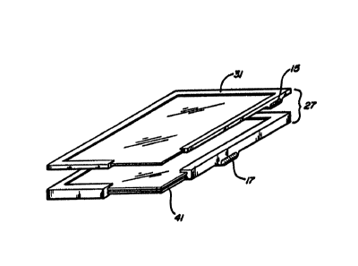
Paperless telefacsimile means 27 includes
position sensitive input means 31 and display means
41. The position sensitive input means 31, as
described herein below, may be an individual element
31 adapted to be collocatea with display means 41, as
shown in Figure 2A.
Alternatively, the position sensitive input
means 31 may be a coating or layer on the display
means, as shown in Figure 2B.
Input/output interface means include sensor
output interface means 15 and display input interface
means 17.
The individual elements of the
teleconferencing unit are described in Section 2 and 3
below, and the integrated unit, with its interactions
and interface unit and elements is described in
Section 4, below.
2. Touch Sensor
The improved, solid state, touch sensitive
position sensor used as the input device of the
instant invention is indicated generally in Figure 3
by the reference numeral 111. The position sensor 111
30 depicted in Figure 3 incluaes a generally
rectangularly-shaped, electrically conductive, exposed
surface 121 that is specifically adapted for detecting
and signalling the X-Y coordinate location of a touch
point 131, such as the finger of a user or a stylus,
placed in contact with the surface 1~1.
In order to accomplish the function of touch
~DS-lll.l -17- t 3 0 8 7 q ~
point 131 location detection, the position sensor 111
includes at least two sets of current diStributiGn and
collection means, generally 141. The current
distribution and collection means 141 establishes a
uniform linear electric field across the conductive
surface 1~1 thereof. i~ore specifically, the electric
field distribution is established by a first
elongated, current distribution means l~la, disposed
along at least one boundary of the conductive surface
121 (such as the lower horizontal boundary thereof)
and a first, elongated, current collection means 161a
operatively disposed along at least a second boundary
of the conductive surface 121. The current
distribution means 151a and the current collection
means 161a are parallel to and face each other on the
conductive surface 121. The first set of current
distribution and collection means, l51a and 161a are
operatively disposed along two opposite boundaries of
the conductive surface 121 of the position sensor 111
and are adapted to cooperatively provide a
substantially uniform, linear electric field
distribution of substantially parallel equipotential
lines E (see Figure 4) across the conductive surface
121. In a preferred embodiment, as described
hereinafter, the current distribution and collection
means are formed as distributed diodes, though other
devices may be employed with equal success.
In the rectangularly-shaped, touc~l sensitive
position sensor 111 illustrated in Figure 3 the first
30 horizontally disposed current distribution means 151a
and the first horizontally disposed, but vertically
spaced, current collection means 161a cooperate to
establish a first uniform electric field distribution
wi$h a first set of horizontal equipotential lines.
This provides high resolution means of determining the
y axis coordinate of the touch point. A second set of
ODS-lll.l 1 30~79~
current distribution and collections means 1~1 are
required in order to provide a x axis coordinate
location. More specifically, the second set of
current distribution and collection means includes one
elongate, current distribution and collection means
151b disposed along one vertical boundary of the
conductive surface 121 and a second elongate, current
distribution and collection means 161b disposed along
the opposite vertical boundary of the conductive
lo surface 121, horizontally spaced from said second
current distribution means l51b. The second set of
vertically oriented, spacedly positioned, current
distribution and collection means, 151b and 161b,
cooperate to establish a second set of uniformly
spaced equipotential lines having a second electric
field distribution orthogonal to the equipotential
lines of the first field distribution. This provides
x axis coordinate location determination means of high
resolution.
The current distribution and collection means
151a, 151b, 161a, 161b contain a plurality of current
leads (such as 152a, 152b, 151c ... 15~m; and 16~a,
162b, 162c ... 16~m, 153a, 153b, 153c ... 153m, and
163a, 163b, 163c ... 163m) equally spaced along the
lengths thereof. These current leads provide for the
flow of electrical current through the current
distribution and collection means to the conductive
surface 121 of the position sensor 111, thereby
establishing an electric field thereacross, which
field results in a flow of current between the
oppositely disposed and charged distribution and
collection means (151a and 161a; 151b and 161b). In a
preferred embodiment, the current leads are arranged
in a configuration of approximately 40 lines per inch,
though any given resolution (from ~ lines to 100 or
more lines per inch) may be employed. However, it is
O~S-lll.l -1~- 1 30~7~
to be understood that the number of current leads per
unit length is limited by the requirement that
cross-talk between adjacent current leads rnust be
substantially prevented.
In the current distribution and collection
means, the lateral distance between adjacent current
leads must be such as to provide relatively high
impedance to current flow therebetween, as compared to
the effective impedance path along the conductive
surface 121 of the position sensor 111. In this way
current is preferentially conducted in a direction
other than along the length of the current
distribution and collection means. The resolution of
the touch position sensor 111 (defined as the accuracy
of determining a specific X-Y coordinate location of a
touch input on the conductive surface) is determined
by the uniformity and linearity of the field across
the conductive surface, especially along edges of said
surface nearest the disengaged current distribution
and collection means, wherein the impedance of the
disengaged current aistribution and collection means
must be fairly high to avoid the flow of current
thereinto.
Electrically interconnected with each of the
current distribution and collection means, 151a, 151b,
161a and 161b, are current control means ~not shown).
The current control means sequentially turn on and
off, in alternating manner, the sets of current
distribution and collection means 141. The current
30 control means must be capable of switching from a
substantially on condition to a substantially off
condition, wi-thout allowing any leakage of current
while in the off state.
The touch sensitive position 111 sensor
further includes a resistance means electrically
disposed between said current distribution and
ODS-lll.l 1 30~ $
-2()-
collection means 141 and said bounded conductive
surface 121. It is preferred that the resistance
means be capable of providing resistance substantially
the same as the resistance of the conductive surface
121, and typically within the range of 10 to 1000
ohms, and most preferably 50 to 500 ohms.
Turning now to Figure 5, there is illustrated
therein a schematic view of the touch sensitive
position sensor 111, including current distribution
and collection means 151a, 161a, 151b, and 161b,
having resistance means, generally 14~ attached
between the distribution and collection means and saia
conductive surface 121. The resistance means are
attached to the current leads (such as 15~a, 152b,
152c...) of the current distribution and collection
means. The resistance means are then affixed directly
upon the conductive surface 1~1 of the touch sensitive
position sensor 111.
The exact principle employed in electrically
determining the x-y location of the touch point 131
can be best described as follows. The conductive
surface 1~1 of the sensor 111 is continually scanned
by a stream of discrete scanning cycles. The scanning
cycles are triggered by associated timing means
adapted to correlate the location of a touch point 131
with respect to the distributed electric field.
Specifically, each scanning cycle, of which there may
be approximately 500 per second, (the actual number of
scanning cycles per second is an independent variable
which may be within the range of 10 to 10,000 cycles
- per second) comprises two half cycles; the first half
cycle is dedicated to determining the y-axis touch
point 131 location by energizing the first or y-axis
current distribution and collection means, l51a and
161a, and the second half cycle is dedicated to
aetermining the x-axis location of the touch point 131
ODS-lll.l -21- 1 308798
by energizing the second or x-axis current
distribution and collection means, 51b and ~lb.
Turning now to Figure 6, there is illustrated
therein the waveform of voltages applied to the first
or y-axis current distribution and col1ection means,
151a and 161a and the second or x-axis current
distribution and collection means, 151b and 161b, to
achieve alternating half cycle scanning. From time
to through tl all current distribution and
collection means are held at a 0 volt potential as in
lo the case where the touch sensitive position sensor is
in its off mode. At time tl through t2, in order
to determine the y-axis location of the touch point
131, the current control means associated with current
distribution means 151a and current collection means
161a are switched into an "on" or forward biased
condition by applying voltage of +5v and -5v thereto
respectively. This allows a uniform electric field tO
be distributed across the display sur~ace 1~1 of the
touch sensor. At the same time, (tl thru t~) the
20 current control means associated with current
distribution and collection means lSlb and 161b are in
an "off" or reversed biased condition, as shown in
Figure 6C and 6d, by applying voltages such as -5v and
+5v thereto respectively (when the current
distribution and collection means 151b and 161b are
diodes, the voltages app1ied to the diodes is
substantially equal in magnitude and less than the
reverse bias breakdown voltages of the diodes). Thus,
a uniform electric field is established across the
30 touch sensor-display surface in the y-asix thereof
during the first half cycle of a complete scanning
cycle.
During the second half cycle, the current
control device associated with current distribution
and collection means l51b and l~lb switch the current
ODS-lll.l -2~- 1 30~79~
distribution and collection means 151b and 161b into
an "on" or forward biased condition by reversing the
voltages applied thereto during the first half cycle,
while the current control devices associated with
current distribution and collection means 151a and
161a are switched into an "off" or reverse biased
condition, again by reversing the voltage applied
thereto during the first half cycle. Biasing the
diodes in this way provides for establishing a uniform
lo electric field in the x-axis of the position sensor
121, and thus, allowing for determining the x-axis
location of the touch point 131. It is important to
note that these scanning cycles are continually being
initiated so as to constantly update the location of
all information entered upon the touch sensor-display
surface 121.
The correlation of the location of the touch
point 131 relative to the distributed electric field
is accomplished by position correlation means (not
shown), The position correlation means compares the
instantaneous electrical field and/or current
distribution to the overall field and/or current
distribution, thereby precisely pinpointing the
location of the touch point 131. As illustrated in
Figure 6, the scanning cycles are initiated at all
times while the sensor 111 is in operation, thus
continually updating the status of the input
information. Further, as should be apparent, the
preferred current control device must be capable of
30 being switched from an "off" to an "on" condition.
As mentioned hereinabove, the alternating
electrical fields so established are distributed in
the manner shown in Figure 4 In figure 4, the
equipotential lines E are substantially parallel. It
is necessary to obtain this high degree of field line
parallelism and orthogonality in order to provide an
ODS-lll.l -2~- 1 30~7 J~
electric field of sufficient linearity an~ uniformity
for determining the precise location of the x-y
position of data input upon the touch sensitive
position sensor.
The high uniformity required for high
resolution determination of the touch point location
(3) requires one or more of highly uniform diode
structure, a high resistance surface 121, or the
reduction of "bulk resistance" effects in the
distributed diodes. Thus, it is possible to increase
the resistivity of the touch sensor-display surface
121 of the sensor lll so as to insure that the diodes
disposed on the touch sensor-display surface l~l will
all operate below the onset of bulk limited behavior.
The resistance of the display surface 12l may easily
be increased, for example, by increasing the amount of
oxygen present in it, thereby making it more
glass-1ike, and there~ore more insulative. A
preferred value for resistance of the conductive
surface 121 of the position sensor lll is a resistance
within the range of 2~ to 5000 ohms per square, and
preferably within the range of l~0 to 300 ohms per
square.
Turning to Figure 7A illustrates the I-V
curve of two similar diodes l~0 and 182. The
difference in I-V characteristic observed for diodes
180 and 182 is attributable to minor thickness
variations (i.e., greater than 1% and less than 5~) in
the fabrication of the diodes. The resistance of the
30 conductive surface l~l, to which the dioaes 18~ and
182 are associated, is represented by line 184. Line
184 passes through the linear portion of aiode 1g2's
I-V curve, and through the bulk limited region of
diode 180. This lack of uniformity of diode I-
~characteristic results in the resolution problems
discussed hereinabove. However, solved by increasing
ODS-lll.l 1 3 0 8 7 ~ ~
-2~-
the resistance of the conductive surface, as indicated
by line 18~ (in phantom) so that less current flows
across the conductive surface and therefore
substantially all diodes associated with the
conductive surface are operating in the linear portion
of their characteristic I-V curve.
Alternatively or additionally a second method
by which to re~iieve the prob'lems of low resolution
associated with the operation of the distributed p-i-n
lo diodes in the bulk limited region, requires that diode
thickness, which is typically in the range of 500 to
15,000 angstroms, be reduced e.g., by approximately
one half, with substantially all of the reduction in
thickness taken from the intrinsic region. Reducing
the thickness of the intrinsic region curves, the
onset of bulk limited behavior to occur at higher
voltage levels, thereby allowing for greater field
uniformity. Figure 7B illustrates the characteristic
I-Y curve for four p-i-n (or n-i-p) diodes~ 180, 18~,
l9~ and 192. Diodes l90 and 19~ are fabricated with
intrinsic layers substantially thinner (i.e., 50~
thinnerj than the intrinsic layers found in diodes 180
and 182 intrinsic layers, thus resulting in I-V curves
characterized by substantia11y longer linear regions.
This results in a characteristic load resistance for a
conductive surface 121, as i'llustrated by line 186
which will pass through the linear portion of a
diode's characteristic I-V curve, as diode l9~ or
192's characteristic curve, thereby eliminating the
30 above discussed problems associated with diode
non-uniformity.
The current distribution and collection means
141 may be formed as an off-stoichiometric silicon
nitride switch, specifically adapted to prevent the
deleterious effects of electrostatic discharge.
Alternatively, the current distribution and collection
ODS-lll.l -25- 1 ~ 0 ~7 q 8
means 141 may be formed as an elongatea, distributed
diode 161D~ which distributed diode is shown in Figure
8. Such an elongated distributed diode 161b is
preferably formed by a plura1ity of superposed,
continuous thin film layers of semiconductor alloy
material deposited upon a common substrate 1~4 of, for
example stainless steel. More particularly, the
distributed diode may be affixed directly to one
boundary of the conductive surface 121 of the position
sensor 111, as by an electrically conductive adhesive
layer 172. The diode affixed to the first boundary
includes consecutively a suDstrate 164 upon which
there is successively deposited: a layer of p-type
amorphous silicon alloy material 165, a layer of
substantially intrinsic silicon alloy material 167, an
n-type layer of amorphous silicon alloy material 169
and a layer of a thin film, electrically conductive
oxide material 171. On the opposite boundary of tne
conductive surface 121 of the sensor, the distributed
diode will also be affixed, but the layers of
semiconductor material will be deposited in reverse
order. Specifically, upon the substrate 164 there is
successively deposited a layer of n-type amorphous
silicon alloy, a layer of intrinsic semiconductor
alloy material, a layer of p-type semiconductor
ma~erial and a layer of thin film conductive oxiae
material, (this reverse embodiment is not
illustrated). It should be appreciate~ that in this
manner, one bounded surface will have an elonga-ted,
3c distributed P-I-N diode disposed therealong while the
opposite bounded surface will have an elongated,
distributed ~-I-P diode disposea therealong. With
this arrangement, one set of the opposed élongated
diodes can be forward biased to provide for
unidirectional current flow across the conductive
surface and the other set of opposed elongated diodes
ODS-lll.l
-26- 1 308798
can be reverse biased to prevent the current flow
across the conductive surface.
An example of the conductive oxide material
employed herein is indium tin oxide, the sheet
resistance of which can be tailored relative to the
sheet resistance of the electrically conductive
surface 121 of the touch position sensor 111 so as to
provide relatively high latera~l resistivity along the
length of the diode, and so as to provide for uniform
lo diode performance. The total thickness of the single
or tandem PIN diode structure is only about 500-15,000
angstroms and preferably 1,0~0 to 8,000 angstroms, and
may also be tailored to provide for uniform diode I-V
characteristics. Further, due to its lateral
resistivity, the single, elongated, distributed diode
may be regarded as a plurality of discrete diode
structures, such as 161ba, 163bb, 161bc,...161bz. The
horizontal separation between each of these discrete
diodes is great enough to provide a sufficiently high
impedance to current flow therebetween so that the
current distribution and collection means 161b will
exhibit preferential current con~uction through the
bulk of the distributor (in a path taken perpendicular
to the conductive surface lZl of the sensor 111). The
lateral resistivity of the conductive oxide must be
high enough so that when that diode structure is not
in an engaged, conductive or "on" mode, the conductive
oxide does not distort the field flowing perpendicular
thereto. It is important to note, diodes of the type
: 30 described hereinabove may be patterned by stan~ard
etch techniques so as to form, for example, a
plurality of individual diodes. Alternatively~ the
conductive oxide surface above may be patterned to
affect electrical communication with adjacent
structures.
Turning now to Figure 9, there is illustrated
ODS-lll.l -27- 1 308798
therein a cross-sectional view of the attachment of
the current distribution an~ collection means 141 with
said resistance means 14~ to the conductive surface
121. Specifically, disposea upon current lead 15~a,
of current distribution means 141 is a resistance
means 142, which may be for example, a discrete thick
film resistor screened or printed thereupon. The
resistance means 142 and current lead 15~a are then
attached to the conductive surface 121 by means of a
layer of electrically conductive adhesive 143.
Specifically, the adhesive must be electrically
conductive in a first direction and electrically
resistive in at least a second direction perpendicular
to the path of electrical conductivity. A material
particularly adapted to this function is manufactured
by Uniax under the trademark "UNIAXIAL CONDUCTIVE
ADHESIVE". A second material manufacture~ by ~M
Corporation and known as 9702 Conductive Adhesive Tape
may also be employed.
Alternatively, the distributed diodes
described hereinabove may be placed in electrical
communication with the surface of the touch sensor
111. In a preferred embodiment, the material utilized
for such a function is fabricated from a thin layer of
an electrically resistive polymeric matrix material
having thin electrically conductive carbon lines
printed thereupon. Particularly well suited materials
for this function are sold by Chinitsu under the
trademark "E L FORM". "E L FORM" matrix is also
adapted to function as the resistance means in that
the "E L FORi~" matrix possesses an inherent electrical
resistance of approximately gO ohms, a resistance
sufficient to enhance and promote field uniformity and
linearity. It is understood however, that other
connection means (with or without associated
resistance means) may be equivalently employed. It is
ODS-lll.l 1 3 3 ~ 7 9 8
-~8-
to be noted that the current distribution and
collection means provides a rectifying junction at
each contact point. This can be accomplished by
depositing a PIN diode structure on one
rectangularly-shaped sheet of substrate material and
depositing a NIP diode structure on a second
rectangularly-shaped sheet of substrate material. The
conductive oxide layer of the PIN diode structure is
electrically connected to the conductive lines of the
lo "E L FORM" matrix, said "E L FORM" matrix being
affixed to one boundary of the sensor 11; while the
conductive oxide layer of the NIP diode structure is
electrically connected to the conductive lines of "E L
FORM" matrix at the opposite boundary of the sensor.
In this manner, current can flow across the conductive
surface 111, but the adjacent diodes (equal in number
to the number of current leads) are unable to
cross-talk. It must be emphasized that only thin film
deposited semiconductor technology can provide for
this type of elongatea distributed diode structure
wherein diodes of opposite polarities are affixed to
opposite boundaries of the sensor 111.
A further advantage realized by employing
thin film semiconductor technology is that diodes
deposited as continuous thin film layers of
semiconductor alloy material are manufactured with
substantial uniformity. The uniformity arises from
the fabrication of an elongated strip of distributed
diode material in a continuous process, under uniform
30 deposition conditions and utilizing substantially
identical precursors. This elongated strip of
multilayered, thin film semiconductor alloy material
can then be cut into smaller strips of a desired size
and shape.
The touch sensitive position sensor 111 of
the instant invention includes means for generating an
ODS-lll.l -2g- 1 30~79~
electrical signal which is indicative of the X-Y
location of the touch point 131. For example, a pixel
or picture element may be addressed in either vector
or matrix coordinates; and a contents co~e, e.g., a
contents code for binary data, or a contents code word
indicative of analog data, such as color, pitch, hue,
gray scale or the like, generated.
The erasure of data inputted onto the
conductive surface of the position sensor may be
lo handled in a manner analogous to the entry of colore~
data. More particularly, the erasure means is adapted
to generate a unique signal so as to provide a signal
of varying strength or frequency. This frequency is
readily sensed by the downstream processing apparatus
as relating to the erasure, vis-a-vis, the entry, of
data and the digital data is removed from memory.
3. Display
.
The paperless facsimile means of the
invention inc1udes means of displaying the image data
entered on the touch position sensor lll and received
from remote data entry points. The display means is a
light influencing display, and preaerably an active
matrix light influencing display.
The light influencing display ~lO has a
plurality of individually addressable picture
elements, cal1ed pixels. Each pixel has a separate
pair of opposing pixel electrodes, with light
influencing material between them. Voltages are
selectively applied to the electrode pairs, causing
the light influencing material between the electrode
to emit light or to change optical density. These
opposing pixel electrodes may be located on opposing
substrates, such as opposing glass pates, ~Jith the
light influencing material, such as liquid crystal
ODS-lll.l 1 308798
-3U-
material, located between the substrates.
Alternatively, the electrodes may be on the same
plate, with the liquid crystal material above or below
them.
In displays with many pixels it is necessary
to use x-y matrix addressing. In x-y matrix
addressing all of the "first" pixel e1ectrodes of a
given row are connected to an address line associated
with that row and all the "second" pixel electrodes of
a given column are connected to an address line
associated with that column. This enables each pixel
to be address by selecting its associated x and y
address lines.
In relatively small x-y light influencing
displays, passive matrix switching is used. In
passive matrix switching each of the x and y lines is
usually directly connected, without intervening
electronic devices, to the pixel electrodes in its
associated row or column In sequential scanning the
pixels of a passive matrix array are driven
sequentially in a scanning process in which each row
is selected successively, and, during the selection of
each row, each column is selected successively. This
causes each of the pixels of each row to be scanned in
sequential order. During the time allotted for the
selection of each pixel the circuitry decides whether
that pixel is to be turned on or off by controlling
the amplitude of the voltage applied across the
pixel. In parallel scanned passive arrays each of the
30 rows is selected in succession, and during the
selection of a row all of the column lines are driven
in parallel with indiviaually selected voltages,
turning each pixel in the row to a desired state,
either "on" or "off". Such passive matrix
multiplexing scanning schemes in which the pixels are
driven directly by their x and y address lines without
UDS-lll.l 3 1 3 0 ~, 7 9 ~
-- 1 --
intervening electronic devices work well for
relatively small arrays. But as array size grows, the
amount of time for the application of a voltage to a
given pixel, or row of pixels, decreases. As a
result, the percentage of time during each scanning
cycle that a given pixel has a voltage applied across
it decreases, thereby decreasing the average contrast
between its "on" state and its "off" state. For this
reason large passive matrix multiplexed displays tend
lo to produce images with poor contrast, making such
displays difficult to read.
One way of overcoming this limitation which
we prefer in the paperless facsimile means of the
teleconferencing system is to use active display
matrixes instead of passive displays. In active
display matrices each of the pixels has associated
with it a non-linear electronic device which acts as a
switch. This switch enables current to flow to or
from the pixel during the brief period when the pixel
is selected, enabling the pixel to rapidly change
state from "off" to "on", or vice versa, but the
switch prevents current flow to or from the pixel when
the pixel is not selected. In this way the charge
placed on the pixel during its brief selection period
is substantially maintained during the rest of the
scanning cycle. As a result, the pixel tends to
maintain its "on" or its "off" state during the entire
scanning cycle, greatly increasing the contrast an~
readabili~y of the display.
The non-linear device that is the swi~ch, may
be a two-terminal device, as a diode, or a
three-terminal device, as a transistor.
a. Display Element ~ith Two-
Terminal Control Devices
ODS-lll.l 1 33~7~8
-3~-
A two-terminal control device is one that has
two current path electrodes and a junction
therebetween.
The junction has a barrier ~leight wllich
allows current flow in one direction but blocks
current flow in an opposite direction.
Figures 10 and 11 illustrate a display pixel
210. Although just one display pixel 210 is
illustrated, it can be appreciated that many such
pixels arrayed in row and column arrangernent are
necessary to provide a complete liquid crystal aisplay.
The display pixel 210 includes an insulative
substrate 212 which can be formed from glass, for
example. Formed on the substrate 212 is an
interconnect bus or lead 214 and a first address lead
216. The interconnect lead 214 and first address lea~
216 can be formed from a conductive material such as a
metal, for example, aluminum, molybdenum, or a
molybdenum tantalum alloy, chromium, tantalum
tungsten, palladium or platinum.
The display pixel 210 further includes a pair
of diodes 218 and 220 formed on the interconnect leads
214 and first address lead 216, respectively. The
diodes 218 and 220 are preferably formed from a
deposited semiconductor material. The deposite~
semiconductor material is preferably an amorphous
semiconductor alloy including silicon. The amorphous
silicon alloy can also include hydrogen and/or
fluorine and can be deposited by plasma assisted
30 chemical vapor deposition, i.e. glow discharge. The
diodes 218 and 2~0 preferably have a p-i-n
configuration formed by a first aoped region 218a and
220a, which can be p-type, an intrinsic region Zl~b
and 2ZOb overlying the first doped regions Z18a and
220a respectively, and a second doped region ~18c and
220c, which can be n-type, overlying the intrinsic
ODS-lll.l 1 30879~
regions 218b and 220b respectively.
The display pixel 210 further includes a
second address lead 226 in electrical contact with the
n-type region 218c of diode 218 and a first electrode
2Z8 which is in electrical connection with the
interconnect lead 214 through the opening 2~4 and the
n-type region 220c of diode 220.
The address leads 21~, 226 are for~ed of
deposited metal essentially parallel to one another,
as can be seen from Figure 11, and both are coupled to
the first electrodes 228. The diodes 21~,220 form an
isolator coupled to the first eleclrode 228. The
isolator formed of the diodes 218, 220 has first and
second inputs to which the address line 226, 216
respectively are coupled.
The first electrode 228 can be configured in
a square configuration as illustrated in Figure 11 and
can be, for example, 30~ microns to Z,OOO microns on a
side depending on the overall size of the finished
display matrix and the desired aspect ratio.
With the first electrode 228 contacting the
interconnect lead 214 through the opening 224, the
diodes 218 and 220 are connected together in series
relation. As shown in Figure 10, the address lead 21o
and 226 are only in electrical connection with the
first electrode 228 through the diodes 218 and 220.
Overlying the resulting structure described
above, is a layer of light influencing material 230.
The display pixel 210 further includes a top
30 transparent insulative plate 232 formea from, for
example, glass. On the inner surface 234 of the
insulative plate 232 is a layer of transparent
conductive material 236 which can be, for exa~ple,
indium tin oxide. The indium tin oxide layer 236
forms a second electrode of the display pixel 210.
This electrode 236 is in contact with the liquid
ODS-lll.l
-34- 1 ~0~798
crystal material 230. The second electrode ~36 is
configured to have the same dimension as the first
electrode 228 and is aligned therewith. The top
insulative plate 232 is polarized in a manner well
known in the art consistent with the type of liquid
crystal display material (light influence material
23~) utilized in the display pixel 210. An alignment
coating of a conventional type can be applied over the
first electrode 228 for the purpose of aligning
molecules in the liquid crystal display material 230.
Figure 12 illustrates the equivalent circuit
diagram of the pixel ~10 of Figure 10. The pixel 210
includes the address leads 216 and 226, a pair of
series connected diodes 21~ and 220 coupled bet~een
the address leads 216 and 226, and the first
conductive electrode 228 coupled between the diodes.
The pixel 210 further includes the second electrode
236 spaced from the first electrode 228. In between
the electrodes 2Z8 and 236 is the liquid display
material 230.
The useful life of a nematic liquid crystal
display can be extended if the polarity of the applied
voltage potential is reversed during alternate frames
or scans. This can be accomplished with the pixel 21
of Figure 10 by impressing a positive potential onto
first address leads 216 and a negative potential onto
the second electrode 236 during one frame to forward
bias diode 220 and by impressing a negative potential
onto the second aadress lead 226 and a positive
30 potential on the second electrode 236 during the next
frame. ~epeating this sequence causes the potential
applied to the liquid crystal display material to be
reversed during alternate frames.
Figure 13 illustrates another liquid crystal
display pixel 240. The pixel 240 incluaes two pairs
of diodes and is formed by first and second
ODs~ 3 0 ~ 7 9 8
-35-
subassemblies 242 and 244 respectively.
Each of the subassemblies 242 and 244 are
substantially identical to the portion of the liquid
crystal display pixels 210 of Figure 10 beneath the
liquid crystal display material 230.
The first subassembly 242 includes an
insulative substrate 252 which can be formed from, for
example, glass. The first subassembly 242 further
includes an interconnect lead 254, a first address
lead 256, and a first pair of diodes 25~ and 2~ wl-ich
can be substantially identical to the p-i-n diodes 218
and 220 of pixel 210. Between the diodes 2~8 and 260
and defining an opening 264 communicating with the
interconnect lead 254 is a layer of insulative
material 262 which can be a polyimide, for example.
The first subassembly 242 further inclu~es a second
address lead 266 and a first electrode 268.
The second subassembly 244 also includes an
insulative substrate 272, and interconnect leads 274,
a first address lead ~76, a second pair of diodes ~78
and 28~, an insulating layer 2~2 defining an opening
284 communicating with interconnect lead 274, a second
address lead 286, and a second electrode 28~. If the
liquid crystal display material 27~ between the
subassemblies 242 and 244 is to be viewed through the
second subassembly 244, then the second electrode
should be formed from a transparent conductive
material, such as, for example, indium tin oxide, and
the insulative substrate 272 should be formed from a
30 transparent material such as glass which is polarized
in a manner consistent with the liquid crystal display
material 270 utilized between the subassemblies. It
will be understood that conventional molecular
alignment coatings and polarizers will be incorporated
into the subassemblies, such as 242 and 244, disclosed
herein as would be known to those of skill in the art.
ODS-lll.l -3b- 1 3 0 o 7 q ~
Figure 14 illustrates the equivalent circuit
diagram of the pixel 24~ of Figure 13. The pixel ~4U
includes a first pair of diodes 258 and 260 and a
second pair of diodes 278 and 2~. Each pair of
diodes is coupled in series relation~ The pixel 240
further includes a first pair of address leads 25~ and
266 coupled to the respectively ends of the series
coupled diodes 258 and 260 and a second pair of
address lead 276 and 286 coupled to respective ends of
lo the other pair of series coupled diodes 278 and 2~0.
The first electrode 268 is coupled to the junction of
the diodes 258 and 2~0 and the second electrode 2~8 is
coupled to the junction of the diodes 27~ and 280.
Liquid crystal display material 270 is disposed
between the electrodes 268 and 288.
The potential applied to the liqui~ crystal
material 270 can be reversed during alternate frames.
During one frame, a positive potentia'l can be applied
to address lead 276 and a negative potential to
address lead 266. During alternate frames, a positive
potentia'l can be applied to address lead 256, and a
negative potential to address lead 28~. In this
manner, the potential applied to the liquid crystal
material 270 can be reversed during a'lternate frames.
Figure 15 illustrates a further liquid
crystal display pixel 2gO. The pixel 29~ is formed on
an insulative substrate 292, such as glass, for
example. Formed on the glass substrate 292 is a first
address lead 294. The first address lead 294 can be
3c formed from a conductive metal as in the previous
embodiments and can be, for example, aluminum,
molybdenum, or molybdenum tantalum alloy, chromium,
tantalum tungsten, palladium, or platinum.
The pixel 290 further includes insulating
layer 296 and insulating portions 304. The insulating
layer 296 and portions 304 can be formed from any
ODS-lll.l
~37~ 1 30~7q~
deposited insulator such as silicon oxide or silicon
nitride. The insulating layer 29~ has openings 306,
308, and 310 therein to expose surface portions of the
n-type regions of the diodes 300 and 302 and a surface
portion of the first interconnect lead 298.
The pixel 290 further includes a bottom
electrode 312 and a second interconnect lead 314.
Figure 15 further shows that the second
interconnect lead 314 contacts the address lead 294
and the n-type region 300c of diode 300 through tne
opening 306 of the insulating portions 304. The
bottom electrode 312 contacts the first interconnect
lead 298 through the opening 308 and the n-type region
302c of diode 302 through the opening 310. The anode
of diode 302 is coupled to the cathode of diode 300
and the anode of diode 300 is coupled to the cathode
of diode 30~. Also, the joint connection between the
anode of diode 300 and the cathode of diode 30~ is
coupled to the first or bottom electrode 312.
The pixel ~Y0 further includes an insulative
transparent plate 316 which has a transparent
con~uctive material 318 deposited on tts inner surface
to form the second electrode of the pixel 290. The
transparent conductor 318 is configured to have the
same dimensions as the effective dimensions of the
bottom electrode 312 and is aligned therewith.
Disposed between at least the electrodes 312 and 318,
and in contact therewith, is liquid crystal display
material 320, which can be, for example, nematic
liquid crystal material of the type well known in the
art. The top transparent plate 316 as well as the
lower plate 292 can be, as in the previous
embodiments, polarized in a manner consistent with the
type of liquid crystal display material 320 utilized
in the display.
Figure 16 illustrates the equivalent circuit
ODS-lll.l
~3~~ 1 30 ~7 ~ 8
diagram of the liquid crystal display pixel 290 of
Figure 15. The pixel ~90 includes the pair of diodes
300 and 302 with the cathode of diode 300 and the
anode of diode 302 coupled together and also coupled
to the first address lead 294. The anode of diode 300
and the cathode of diode 302 are also coupled together
and to the first electrode 312. The second electrode
318 is coupled to a second address lead 322 (not shown
in Figure 15) and the liquid crystal display material
320 is disposed between and in electrical contact with
at least the electrodes 312 and 318..
The potential applied to the liquid crystal
material 320 can be reversed during alternate frames.
During one frame, a positive potential can be applied
to first address lead 394 and a negative potential to
second address lead 3~2. During alternate frames, a
positive potential can be applied to second address
lead 322, and a negative potential to first address
lead 294. In this manner, the potential applied to
the liquid crystal material 2~0 can be reversed during
alternate frames.
Figure 17 illustrates a further alternative
display useful in the present invention. A single
pixel 340 of a display which incorporates a
subassembly 342 is illustrated in Figure 17. Spaced
apart from the subassembly 342 is an insulating
transparent substrate 344 which can be formed of
glass and upon which is formed a pixel electrode 34~.
The pixel elecirode 346 may be formed of transparent
30 indium tin oxide. Between the substrate 344, the
pixel electrode 346 and the subassembly 342 is a
region 348 which is filled with a light influencing
material. For example, nematic liquid crystal
material of a conventional type may be used.
The subassembly 342 includes an insulating
substrate 350, such as glass, upon which is formed a
ODS-lll.l 3~ l 30~79~
pixel electrode 352. The subassembly 342 also
includes a first address line 354 formed on the
insulating substrate 350 and a second address line 356
insulated from the first address line 354 and carried
by the insulating substrate 350. An isolation device
358, preferably a p-i-n diode, is formed on a region
of the first address line 354. A silicon dioxide
layer 360, or equivalent insulator as previously
disclosed, surrounds the diode 358 and covers the
first address line 354 except in a region or via 3~2.
A metal deposit 364 extends through the via 362 and is
in contact with the isolation device 358. The metal
deposit 364 couples the isolation device 358 to the
pixel electrode 352.
A second isolation device 366, also
preferably a p-i-n diode, is formed on a region of the
pixel electrode 35~. An insulating layer 36~, such as
silicon dioxide, surrounds and covers the isolation
device 366 except in a region or via 37~. A metal
deposit 37Z extends through the via 370 to contact the
isolation device 366. The second address line 356 is
preferably formed during the same processing step and
at the same time as the metal deposit 372. To
simultaneously form the second address line 356 and
metal deposit 372, a layer of metal can be deposited
over the insulating layer 368. The metal layer is
then etched away in a conventional fashion to form the
deposit 372 and the second address line 356.
Alternately, the second address line 356 could be
formed before or after the metal deposit 372. The
metal deposit 372 couples the isolation device 3~6
between the pixel electrode 352 and the second address
line 356. The second address line 356 is deposited on
a region of the insulating layer 368. The equivalent
circuit of Figure 12 applies to the liquid crystal
display 340 of Figure 17.
ODS-lll.l 40 1 30~7q~
The address lines 354, 356 are for~ed with no
crossovers as were the address lines ~16,~26. The
address lines 354,356 are each coupled to the pixel
electrode 35~.
b. Display Element With Three-
Terminal Control Devices
Alternatively, the active matrix may have
lo three-terminal non-linear control devices.
A three-terminal control device is one that
has two current path electrodes and a control
electrode, with the effective resistance between the
two current path electrodes being controlled as a
function of a signal supplied to the control
electrode. For example, in the thin film field effect
transistors often used in active matrix displays, the
voltage applied to the gate electrode controls the
amount of current wnich flows between the source and
drain electrode of the transistor.
Pixel electrodes of one polarity, the
associated X and Y address lines, and the associated
three-terminal devices are deposited on one substrate
of the display. Each of the three-terminal devices
has one of its current path electrodes connected to
pixel electrode of the associated pixel. The X and Y
lines are on the substrate to enable each
three-terminal device and its associated pixel to be
individually addressed. One of the sets of the
address lines, for example, the X address lines, are
connected to the control electrodes of the three
terminal devices, with an X address line being
connected to all of the control electrodes (gate) in
one row of pixels. Correspondingly, the other set of
address lines~ for example, the y address lines, are
connected to one of the current path electrodes
ODS-lll.l 1 3087q~3
-41-
(source or drain) of the control devices, with a Y
address line being connected to a current path
electrode (source or drain) of each pixel in one
column of pixels. The pixel electrodes on the
opposite substrate are usually connected to a common
voltage, such as grouna.
An individual pixel is switched by applying a
voltage above a threshold voltage across the liquid
crystal material of the pixel. This is accomplished
by applying a potential, i.e., a gate voltage, to the
X address line connected to the control electrode of a
three-terminal device and simultaneously applying a
potential, i.e., a drain potential, across the Y
address line connected to the current path electrode
of the three-terminal device. For example, when the
three-terminal devices are thin film field effect
transistors, the gate o~ each transistor is connected
to an X address l;ne and the source of each transistor
is connected to a Y address line. In a field effect
transistor, the pixel is switched, i.e., structure, a
selected is turned on or off by applying the
appropriate voltages between to the X address line
connected to its gate and the Y address line connected
to its source.
A typical light influencing display, useful
in providing the display of the integral, modular,
input and display and the mode of operation of the
display are shown in Figures 18 througn 25.
Figure 18 shows a schematic diagram of a 3 X
30 3 pixel array. The circuit elements formed on the
bottom substrate are shown by solid lines and the
circuit elements formed by the strip conductors 544 on
the upper substrate 542 are shown by dotted lines.
The gates 524 of the transistors are connected to the
x address lines 530 while the drains 526 are connected
to the y address lines 544 through the pixel
ODS-lll.l -42- 1 30879~
electrodes 520 and pixel 551. The sources 528 of all
of the transistors 522 are connected to ground through
the second conductive leads 532.
Figure 19 shows the voltage waveforms applied
to the circuit shown in Figure 18 to cause the
individual pixels to form the pattern shown in Figure
20. For purposes of illustration only, the pixels 551
are light transmissive unless a voltage is applied
across them. When a voltage is applied across a
lo pixel, the pixel becomes light blocking or dark. The
waveforms Xl, X2, and X3 are voltage waveforms
which are supplied through the control leads 530 to
the gates 524 of the transistors in the rows 514, 515
or 516, respectively. Similarly the waveforms Yl,
Y2 and Y3 are voltages applied through strip
conductors 544, which function as data leads, to the
pixels 551 in the columns 517, 518 and 519,
respectively. The Y voltages are applied through the
pixels to the drains 526 of the transistors 522. The
20 source electrodes 5~8 of all the transistors 52~ are
connected through the voltage supply leads 532 to
ground.
In operation, each of the transistors 522 in
a given row 514, 515, or 516 is turned on when its
respective X address line 530 is supplied with a
positive "on" gate voltage, which for the TFTs of the
illustrated embodiment is approximately 1() volts.
Once the transistors 522 of a given row are turned on,
the conductivity between the sources 5~8 and drains
30 5~6 of that row is greatly increased, effectively
connecting the bottom pixel electrodes 520 of that ro
to ground. When a given row is selected in such a
manner, a plurality of selected data voltages are
applied in parallel to the second pixel electrodes of
the row by means of the data leads, or Y lines 544.
This causes each of the pixels 551 in the selected row
~DS-lll.l 43 1 30~798
to be charged to a voltage equal to the difference
between the data voltage on its associated Y line and
the ground voltage on its source line 532. For
example, during the first third of each p-mode, when
the address line Xl is high, the Y address line Yl
is supplied with an "on" data voltage of approximately
+5 volts, and the Y address lines Y2 an~ Y3 are
supplied with "off" data voltages of zero volts. As a
result, the left pixel of the top row is turned on,
lo whereas the remaining two pixels of that row remain
off. In the embodiments described in Figure ~, the
pixels which are turned on are made opaque or dark,
and the pixels which are left off remain transparent
or light. It is to be understood, however, that the
circuitry is also applicable to displays which behave
just the opposite, that is, in which pixels that have
a voltage applied across them turn transparent and
those without a voltage applied across them remain
opaque.
2~ During the period when the first row is
selected and has its transistors turned on, the
address lines X2 and X3, which are connected to
the other non-selected pixel rows, are supplied with a
negat;ve potential of -5 volts. This negative
potential extends below ground by -5 volts and insures
that each of the transistors in non-selected rows
remain off. In fact this voltage is su~ficient1y low
to insure that the transistors in non-selected rows
remain off, even when the voltage on their assoeiated
3Q bottom pixels 520, which are connected to their drains
526, is less than ground by twice the "on" pixel
voltage of 5 volts. This is necessary for the
following reason. If a given pixel is charged to +5
volts when its row is selected by placing its bottom
pixel electrode 520 at ground and its Y line at +5
volts, this charge causes its bottom pixel electrode
ODS-lll.l 1 3 0 ~ 7 9 8
to remain 5 volts below the voltage on its Y line for
as long as that 5 volt charge remains on the pixel.
Since the leakage of charge across the pixel through
the liquid crystal rnaterial, is relatively small
during the period between the pixel's recharging, and
since the trallsistor associated with the pixel is
supposed to be turned off when its row is
non-selected, a substantial portion of the +5 volt
charge remains on the pixel during the period when it
is non-selected. Thus, if the Y line ~rops to zero
volts during the selection of another row, the voltage
on the pixel's bottom electrode 520 drops to
approximately -5 volts. Even more extreme, if during
the n-mode, described below, the Y line drops to a
minus "on" pixel voltage of -S volts, the bottom pixel
electrode or the address line will drop to
approximately -10 volts. Because this large negative
voltage is connected to the drain, the transistors in
non-selected rows should be supplied with a negative
gate voltage to insure tnat they remain off. Since
the gate threshold voltage of the transistors of the
preferred embodiment is more than 5 volts, the "off"
gate voltage of -5 volts is sufficient to keep the
non-selected transistors off even when the voltage on
their drain reached -10 volts.
In the second third of each p-mode period,
the second X line, X2 is supplied with a positive,
or "on", gate voltage and all the other X lines are
supplied with an "off" gate voltage of -5 volts. As
30 shown in Figure 19, during this period the line Y
is held at zero volts and the lines Y2 and Y3 are
supplied with "on" voltages of +5 volts. Thus, as is
shown in Figure 20, the first pixel in the row X~
remains off, and thus transparent, whereas the second
and third pixels in that row are turned on, and thus
are light blocking. Similarly, during the last third
ODS-lll.l 5 1 30~7~&
of the p-modes, the last row X3 has a positive "on"
gate voltage supplied to its transistors, an~ the
other rows have negative or "off" gate voltages
supplied to their transistors. During this time, the
line Yl is supplied with a zero "off" voltage, the
line Y~ is supplied with a positive "on" voltage and
line Y3 is supplied with a zero "off" voltage.
Thus, the first and third transistors of that row
remain off, and only the middle transistor of that row
o is turned on.
As stated above with respect to two-terminal
devices, it is important to periodically reverse the
polarity of the voltages applied across in~ividual
pixels. For this reason the voltage driving scheme
used to power the display shown schematically in
Figure 18 is divided into alternating positive and
negative modes, indicated by the labels p-mode and
n-mode in Figure 19. In this driving scheme the
voltages applied through the ~ lines, Xl, X~ and
X3 to the gates of the transistors 5~ are the same
during both the p and n modes. However, the polarity
of the voltages applied to the Y lines, Yl, Y2 and
Y3 during the n-mode are reversed in polarity
relative to those applied during the p-mode. Thus the
voltages supplied to the X lines turn on the
transistors of the display in the same manner during
both the p-and n-modes, but during the n-mode the
pixels 551 which are to be turned on are supplied with
a negative "on" voltage of -5 volts, rather than a
30 positive "on" voltage of +5 volts.
The devices alternate between the p-and
n-modes at an acceptable frequency. Typically, the
frequency is 60 times a second, the rate used to
alternate between fields of a standard video signal.
As a result, a pixel which is turned on has the
polarity of the voltage applied across it rapidly
ODS-lll.l 1 30~7q~
-46-
alternated, preventing any net dc current flow through
the liquid crystal material associated with the
pixel. Furthermore, since the entire pixel array has
each of its pixels rewritten, for example, 60 times a
second, there is no perceived flicker on the display.
Figure 21 is a schematic diagram of an
alternate active matrix display useful in the
paperless facsimile of the invention. This embodiment
is identical to that shown in Figure 18, except that
lo the sources 528 of all of its transistors are
connected through voltage supply lines 532 and the
common conductive lead 533 to a variable preselected
voltage supplied by a common voltage supply VCs.
Figure 22 shows the voltage waveforms used to drive
the circuitry of Figure 21 to produce the pixel
pattern shown in Figure 2(~. As is shown in Figure 2~,
the output of the common voltage supply ~cs~ which
is connected to the sources of all the transistors
522, is repeatedly alternated between two voltages, a
more negative voltage ana a more positive voltage.
The output of Vcs is held to a more negative ground
voltage during each p-mode and it is held to a more
positive voltage of +~ volts during each n-mode.
During the p-mode the apparatus shown in
Figure 21 with the waveforms shown in Figure 22
operate identically to the apparatus shown in Figure
18 with the waveforms shown in Figure 19. It is in
the n-mode that the voltage driving schenie shown in
Figure 22 differs from that shown in Figure 19. As
30 described above, the voltage driving scheme shown in
Figure 19 reverses the voltage polarity across the
pixels by switching the polarity of the "on" ~ata
voltages supplied to the Y lines from +5 volts during
the p-mode to -5 volts auring the n-mode. In the
voltage driving scheme shown in Figure 2~, on the
other hand, the change in polarity across the pixels
~ 3 G ,~
ODS-lll.l
-47-
551 is accomplished by both (a.) a change in t~e
common voltage supply Vcs from the more negative
ground voltage to the more positive voltage of +5
volts, and (b.) a reversal of the "on" and "off" data
voltages supplied to the Y data lead lines 544,
changing the "on" data voltage from +5 volts to
ground, and changing the "off" data voltage from
ground to +5 volts. During the n-mode, when the
sources of all of the transistors 522 are supplied
o with the more positive voltage of +5 volts, the Y
lines 544 discharge, or turn off, pixels in selected
rows by supplying the upper electrode with +5 volts,
and they charge those pixels to a negative "on"
voltage by supplying the upper electrodes with zero
volts, which is 5 volts less than tne voltage supplied
to the bottom pixel electrodes in a selected row.
During the n-mode, the gate voltage supplied
on the lines Xl, X2 and X3 to turn on the
transistors of a selected row is +15 volts, which is
higher than the +10 volts used for this purpose during
the p-mode. This is to insure that during the n-mode,
when the sources 528 of the transistors in a selected
row are supplied with +5 volts, the voltage supplied
to the gate 524 of those transistors is sufficiently
higher than that source voltage to keep the selected
transistors fully on.
2eferring now to Figure 23 and 24 an
alternate active matrix display useful in the
paperless facsimile of the invention is shown. Figure
30 23 is a partial top plan view of a bottom substrate
subassembly with the voltage supply and control leads
located between the pixel rows 514, 515 and 516
combined into one common conductive lead 572. This
greatly simplifies the wiring associated with an X-Y
pixel array, reducing almost in half the number of
address lines required on the bottom substrate
ODS-lll.l 1 3037q8
-48-
subassembly in large X-Y array. As is shown in
Figures 23 and 24, the top X line 57~ is labeled X
indicating that it is connected to the gates of the
first row of pixels. The second X line 572 is labeled
Xsl G2, indicating that it is connected to both the
sources of the first pixel row and the gates of the
second pixel row. Similarly, the third X line 572
shown in those figures is labeled Xs2 G3, indicating
that it is connected to both the sources of the second
lo pixel rows and the gates of the third pixel row.
Finally, the bottom most X line 572 is labeled X53
indicating that it is connected to the sources of the
third pixel row.
Jhe bottom substrate subassembly shown in
Figure 23 is combined with the top substrate
assembly. When this is done, the resultant light
influencing display has a circuit diagram shown in
Figure 24, in which each of the bottom pixel
electrodes S20 on the bottom substrate subassembly
forms a light influencing pixel 551 in conjunction
with its associated transparent Y conductive strip
544. The display shown in Figure 24 is identical to
that shown in Figure 1~3 except that the control and
voltage supply lines between its pixel rows have been
combined, as described above.
Figure 25 illustrates the voltage waveforms
which are supplied to the X lines 572 and Y lines 544
shown in Figure ~4 in order to make the 3 X 3 matrix
have the image pattern shown in Figure ~0. The
30 voltages supplied to the Y lines shown in Figure ~S
are identical tP the voltage supplied to the Y lines
shown in Figure 19. Similarly the voltage supplied to
the X line XGl in Figure 25 is identical to that
supplied to the X line Xl in Figure lY. This is
because the X line XGl, being connected only to the
gates of transistors in the row below it, functions
ODS-lll.l
~49~ 1 3087~8
analogously the line Xl in Figure 19. The voltages
sUpplied to the lines Xsl G2 and XS2-G3' howe
are different than those supplied to the lines X2
and X3 in Figure 19. This is because the lines
X5l-G2 and X52_G3 both supply gate voltages to the
row below them and to supply source voltages tO the
row above them. The lines X51-Gl and Xs2 G3 are
capable of performing both functions because these
functions occur at different times.
lo During most of each scanning cycle, the
connection of each of these combined source-gate lines
to the sources of the transistors in the row above it
is without consequence, because the source addressed
transistors are turned off, effectively isolating
their drains and associated bottom pixel electrodes
from the sources. It is only during the brief period
when the source addressed transistors in the row
immediately above such a line are selected by the
application of "on" gate voltages that the connection
of a combined source-gate line, XS Gl, to the
sources of the source addressed transistors is of
significance. During this perioa a zerG or ground
voltage is supplied to the combined source-gate line
so that a ground voltage is supplied through the
selected transistors to their associated bottom row to
charge up to the voltage supplied on its associated Y
address line.
During the rest of the time, wl~en other pixel
rows are selected, the combined source-gate line,
30 Xs G~ acts only as a gate voltage supplying line,
and voltages supplied to it are identical to those
supplied to the corresponding X lines in Figure lg.
'~hen the pixel row directly below a combined
source-gate line is selected, that line is supplied
with an "on" gate voltage of +10 volts to turn on the
transistors of the selected row. During periods in
~DS-lll.l ~0 1 3 0 ~ 7 9 ~
which neither the pixel row directly above nor
directly below a given source-gate line is selected,
the voltage supplied to that given line is held to a
-5 volts to insure that the non-selected transistors
in the row directly beneath it remain off.
During the brief period when a source-gate
line supplies a ground source voltage to the
transistors in the selected row directly above it, it
also supplies a ground gate voltage to the transistors
o in the non-selected row immediately below it. This
undesirably high gate voltage for a non-selected row
has the effect of enabling transistors in the row
immediately beneath the source-gate line to discharge
when the bottom pixel electrodes 5~ connected to the
drains of such transistors are driven to a large
negative voltage, such as -10 volts, as described
above in the explanation of why a -5 volt gate voltage
is normally supplied to the transistors of
non-selected rows. However, this brief period in
which non-selected rows receive a slightly higher than
desired gate voltage has a relatively small effect on
the RMS voltage applied to each pixel over each
scanning cycle. Such a zero volt gate voltage is only
applied to a given non-selected row during the brief
period in which the row directly above it is
selected. In a large display in which there are many
lines, this possible loss of a pixel's charge only one
line interval before it is to be rewritten is of
little concern.
The voltage supplied to the line Xs3 is
held at ground. This is because this line functions
only to supply voltage to the sources of the
transistors in the pixel row immediately above it, and
thus it is free to remain at ground at all times.
4. Integrated Teleconferencing System
ODS-lll.l 1 3 0 ~ 7 9 8
-51-
The individual teleconferencing system
contemplated herein includes a speech circuit, and a
paperless telefacsimile means, i.e., a touch position
sensor, a display, and circuits to provide interaction
therebetween. The touch position sensor and the
display, as well as the speech circuit interact with
each other and interface with the communications
network through internal data processing systems,
including data storage systems, and through
lo interfacing systems. These systems translate analog
touch position sensor current flows and potentials
into digitized touch position locations, store the
digitized touch position location in touch position
location digital memory means, update the digital
memory means, display the updated memory contents data
on the display, transmit either or both of the
instantaneous touch position and/or the updated memory
contents through a communications network to other
output devices, receive inputs to the memory and/or
the display through the communications network from
other input sources, and send and receive speech
communications.
a. Network
figures 26 and 27 are block aiagrams of the
teleconferencing system. In Figure 26, two systems
are shown communicating through an analog data
network, i.e., a telephone network. The display
30 circuit is omitted from one system, and the toucn
sensor is omitted from the other system. This is done
only as a simplification, since each teleconferencing
system includes a complete paperless telefacsimile
system with both a touch sensor and a display.
The touch sensor of the paperless
ODS-lll.l -52- 1 30~798
telefacsimile means includes means for converting
touch point location analog data that is, the unique
set of currents and/or voltages identified with a
touch point location to digital output. This ~igital
output may be stored internally, displayed on the
associated display, or transmitted to a remote
location as a digital computer, a remote display, or a
remote paperless telefacsimile means. The system for
measuring the analog currents and/or voltages of the
touch sensative position sensorand converting the
analog measurements thereof to digital output is
referred to as a touch sensor drive. The ~igitized
output of the touch sensor drive is typically parallel
bit digital data, and must be converted to series
analog data for data transmission over analog, e.g.,
telephone lines, to the remote location. The
conversion from digital parallel data to series
digital data is accomplished in parallel to series
conversion means. The serial digital data is then
modulated, that is converted to analog data, for
example, by a modulator means, for transmission over
the analog communication network to the remote
location. The analog data signal is demodulated and
digitized to a series digital bit stream at the
receiving end, for example, in a demodulator.
Thereafter, the serial digital data is converted to
parallel digital data and the parallel digital data is
then input into a display means where it is displayed,
and also, if desired, entered into a memory means as
30 digital data.
A two unit teleconferencing network is shown
schematically in Figure 26 and one teleconferencing
system is shown schematically in greater detail in
Figure 27. For the sake of simplicity and solely for
purposes of illustration only, and not with any
intention to limit the scope of the invention thereby,
ODS-lll.l 1 3Q879~
-53-
the display 41 is omitted from the transmitting unit
lla of Figure 26 and the tOUCil position sensor 31 is
omitted from the receiving unit 116 of Figure 26.
The output from the touch position sensor
means 31 is represented by parallel bits. While the
parallel bit output can be directly inputted to the
display means, not shown, of the sarne teleconferincing
unit lla, the parallel bit digital output must first
be processed in order to be input to a display means
lo 41 at remote teleconferencing unit 116. This requires
conversion to a serial stream of output bits, for
example, in a parallel to series conversion means 33.
Moreover, if the serial bit stream is to be
transmitted over analog transmission lines, as
telephone network means 57, it must be changed to
analog signals. The analog signals utilized in
commercial telephone networks are electrical signals
at audio frequencies, i.e. 300 Hz to 3,400 Hz.
Similarly, both for receiving and displaying
of the signals at the remote display, and when the
individual teleconferencing unit is in a "receive"
mode, the analog data input stream must be digitized
and, depending on the internal logic of the receiving
display, converted from serial input to paràllel
input.
b. The Indi_vidual Telephone-Paperless
Telefacsimile Unit
Figure 26 shows a pair of teleconferencing
units lla and 116 connected through a network 57.
Figure 27 shows an individual teleconferencing unit
11. The teleconferencing unit 11 has a display 41
including drive means 42, and a touch sensor panel 31
including touch sensor panel drive means 3~. Figure
26 shows one unit lla in a "transmit" mode with data
ODS-lll.l 54 1 3 0 ~ 7 S 8
being entered on the touch position sensor 31 and the
second unit 116 in a "receive" mode with the data from
the touch position sensor 31 of the first unit lla
being displayed on the display 41 of the second unit
llb.
Data is entered on the touch position sensor
31 of the first unit, 11 e.g., by a stylus, a finger
touch, or the like. The data is analog data in the
form of current flows and/or voltages, and is
lo translated into a set of touch points, each touch
point being uniquely defined by a current flow pattern
and/or voltage map. This set of touch points is
digitized, for example, by an analog to digital
convertor incorporated in the drive means 32. The
output of the touch sensor drive means 32 is a data
stream that is representative of touch point
location. This data stream may be a parallel bit
stream or a series bit stream. It is shown in the
figure as an eight bit parallel stream 33.
When the data is recovered ~rom the touch
sensor 31 as parallel data, it must be converted in
parallel to series conversion means 33 to a serial bit
stream 34 for transmission, as will be described
hereinbelow.
The output 34 of the parallel to series
conversion means 33 cannot be transmitted over the
presently existing commercial te1ephone networks 57 as
such. This is because the commercial telephone
network 57 is adapted for analog data at audio
frequencies, i.e., 300 to 3,400 Hz. Thus, the series
digital data 34 must be converted to analog data.
This is accomplished in digital to analog convertor
means, for example, a modulator means 51. While the
digital to analog conversion means and the analog to
digital convertor means at the receiving unit may be
omitted in a data network using ~igital transmission,
.
ODS-lll.l
-55- ~ 30`8~$
the invention herein contemplated is intended for use
in either a ~igital mode or an analog mode, and
therefore is shown and illustrated with the
modulator-demodulator means 51, i.e., a modem, which
must be provided where voice network or other analog
data communication means are employed.
The analog or modulated signal is
demodulated, i.e., converted to a digital data signal,
for example, in a demodulation means 51 at the
lo receiving teleconferencing unit 116, computer,
display, or the like. The demodulated digital data
144 is in serial digital data form and must, if
necessary, be converted to parallel data 45 form.
Conversion from serial to parallel data is
accomplished in a serial to parallel signal conversion
means 43 such as, a UART, a Universal Asynchronous
Receiver Transmitter as described hereinbelow.
The parallel data output 45 of the serial to
parallel conversion means 43 is the input to the
display drive means 4Z of the second unit 116, and Ihe
is displayed as analog data by the display means 41 of
the second unit 11~.
Figure 27, shows a more detailed block
diagram of an individual teleconferencing unit 11.
The teleconferencing unit 11 includes the speech
circuit 21, the touch sensor circuit 31, the ~isplay
circuit 41 and certain circuits, not shown, such as
the pulse or tone dialing circuit, acoustical circuits
(anti-tinkle, muting, and balancing), and the like.
30 The touch sensitive position sensor 31 and the display
41 may have their own respective parallel to series
and series to parallel conversion means 33, 43 as
shown in Figure 27. Alternatively, the touch sensor
circuit and the display circuit may share a common
means for converting parallel bit data to serial bit
data and serial bit data to parallel bit data. There
ODS-lll.l -56- 1 3 0 8 7 ~ ~
are also data bus means 40 or data bus means combined
with suitable data processing means tnat allow the
output of the touch sensor 31 to be direct or
processed input to the associated display means 41 and
directly inputted thereto.
The parallel output 30 of the touch position
sensor 31 is converted to series digital data 34 by
the parallel to series to conversion means 33. The
series output 34 of the parallel to series convertion
lo means 33 associated with the touch position sensor 31
is modulate~, i.e., converted to analog data, for
example, in modulator means 51 and the series input to
the display serial to parallel convertor is
demodulated in demodulating means 51. The modulating
means 51 and demodulating means 51 may be combined
into a single element, i.e., a modulating-demodulating
means or modem. The touch position sensor 31 and
display 41 interact through the modulator-demodulator
means 51 and may interact through data bus and data
storage means 40 which buffer the output of the touch
position sensor 31 as input to the display 41, and
update it with inputs 30 from the touch position
sensor 31 and input 44 from the remote unit 116.
The modulator means and demodulator rneans 51
and 51, for example modems, take digital output from
the UART 33 and modulate it to the analog carrier
signal of telephone network 55. The demodulator means
51 receives a modulated analog carrier signal and
delivers a serial digital display input 44 to the UART
43.
The speech circuit ~1 is well known in tne
art.
A speech and data switch means 53 is
provided. This switch 51, in combination with
asynchronous data transmission and with storage of a
transmitted touch sensor output, allows a form of time
~US-lll.l 1 308798
-57-
domain multiplexed "simultaneous" voice and data
transmission. The switch 57 may be a manual switch,
for example on the touch pad or on the telephone hand
set. Alternatively, it may be a logical switch driven
by a particular duration of the signal, for example
the logical 0, the logical 1, or the carrier frequency
continuously transmitted over the analog network.
While the invention generally and the
multiplexing of voice and data transmissions
o particularly are illustrated with respect to an
asynchronous or "hand shake" data transmission mode
rather than a synchronous or clock controlled data
transmission mode, it is to be understood that the
invention may also be used with synchronous or with
isochronous data transmission. Switching between
sending and receiving modes is unnecessary in the
asynchronous, full multiplex mode because of the
different frequencies utilized. Moreover, in the
asynchronous mode, switching between voice
transmission and data transmission mode may be
accomplished by measuring the duration of a string of
carrier frequency signal only, with a switch to voice
after some preset time of carrier frequncy only, or by
measuring a string of a signal that has frequencies
separate and distinct from either those corresponding
to logical "0" or logical "1", with a switch to the
voice mode after some predetermined duration thereof
or after a predetermined string of unchanging logical
"0" or "1". Alternatively, switching between voice
30 and data may be by a manual switch, or by a unique
signal identified to contact between the stylus 3~ and
the touch position sensor 31.
The interaction of the touch position sensor
31 and the display 41 through the data bus and data
processor 40 allows local and remote display of the
data entered into the touch position sensor 31 as well
ODS-lll.l 1 3 0 8 7 q 8
-58-
as local an~ remote entry of data into the display
41.
c. Parallel To Series Conversion
~ ,_. _ . . . _ . _ .
Various parallel-series conversion means are
known in the art. One we11 known paral1el-series
conversion means is a universal asynchronous receiver
transmitter, also referred to as a UART. The
digitized data may be sent therefrom in any software
compatible code, for example, 5 bit CCITT, 7 bit
ASCII, 8 bit ASCII, and may be sent in even or odd
parity. The connection between the two units may be
synchronous, that is with a common clock means, or
asynchronous, referred to in the art as "hand shake"
communications, or isochronous.
The Universal Asynchronous Receiver
Transmitter (UART) allows reception and transmission
of serial data to be done by hardware rather than
software. Hardware for serial to parallel and
parallel to serial conversion is a Universal
Asynchronous Receiver Transmitter or UA~T. The modern
integrated UART provides separate, independent
transmitter and receiver means for serial data with
two clock inputs to determine the baud rate. The
provision of separate receiver and transmitter
circuits in one unit allows full duplex operation to
take place. An important feature of the UART as it is
interfaced to, for example either or both the touch
position sensor 31 and/or the display 41 is that its
input to the display 41 and its output from the touch
position sensor 31 both appear to the display and
touch sensor pad, respectively, to be parallel, for
example 8 bit parallel data. This is because the UART
simply writes a byte to the parallel output port and
reads a bite from the demodulator input port. The
ODS-~ll.l 5~ 1 3 n87 q 8
UA~T serializes the data, inserts parity bits, and
controls the data rate.
d. Modulation-Demodulation
The interface of the unit 11 with the
acoustical analog telephone network 57 through
interconnect means 55 is determined by the limitations
of the network 57. This is because there is only a
lo limited amount of band widt~l that is practically
available to carry voice communications. At the
present time, the lowest-cost telephone data
communication means are voice ban~ channels adapted
for a band width from 300 Hz to 3,40~ Hz. It is
.therefore necessary to modulate the 300 to 3,400 Hz
carrier frequency to carry the digital image data from
paperless telefacsimile 31-41 of the teleconferencing
lla to the paperless telefacsimile 31-41 of
teleconferencing unit llb. This may be done within
the available band width by modulating the carrier
amplitude, that is, by modulating the amplitude
between a high amplitude for logical "1" and a low
amplitude for logical "0". Alternatively, the
frequency may be modulated, for example, between high
frequency logical 1 and low frequency for logical 0.
According to a still further embodiment, phase of the
carrier may be shifted, for example, shifted in one
direction for a logical 1 and in an opposite direction
for a logical 0. This is a technique known as, "phase
key shifting".
As stated, the available band width is from
300 Hz to 3,400Hz. However, the output from a touch
position sensor pad 31 and the input to a display 41
are high frequency signals. These signals must be
modulated, that is converted to electrical signals
having frequencies in the audible band width in order
1 3087~
ODS-lll.l
-60-
to be carried over the 300 Hz to 3,400 Hz voice
network. More specifically, Figures 28, 25 and 30,
show the frequency spectrum used for data
communication over a voice comrnunication network.
~ith Figures 28 and 29 show the frequency spectrum
usea for low speed asynchronous
modulation-demodulation means, with Figure 28 showing
the frequency spectrum for a simplex or half
transmission mode, and Figure 2~ showing the frequency
lo spectrum for d full duplex transmission mode.
In the simplex or half transmission mode,
that is, the frequency spectrum shown in Figure 28,
the frequency spectrum from 300 to 3,400 Hz is
available for data transmission. A central frequency
of 1,170 Hz is used for the carrier which is shifted
to 1,070 Hz for the logical "O" and to 1,270 Hz for
the logical "1".
In th~ full duplex mode for full two-way data
communication, shown in Figure ~9, the frequency
spectrum of 300 to 3,40~ Hz is again available for
data transmission. This spectrum is divided into two
band widths as shown in Figure 2g. One band width is
a lower frequency band width having a central
frequency of 1,170 Hz. The other band width is a
higher frequency band width having a central frequency
of 2,12S Hz. The lower frequency band width with a
central frequency of 1,170 Hz transmits a logical "~"
by switching to 1,070 Hz and a logical "1" by
switching to 1,270 Hz. The higher frequency band
width with a central frequency fo 2,025 Hz transmits a
logical "O" by switching to ~,125 Hz and logical "1"
by switching to 2,225 Hz.
Figure 30 shows the frequency spectrum for
high speed asynchronous data transmission, for example
l,~OU bytes per second. Although this frequency may
not be necessary for the use of the herein
ODS-lll.l -61- 1 308798
contemplated teleconferencing system, certain
advantages are offered by a design capable of high
speed, asynchronous, full duplex, data transmission.
In the 1,200 bytes per second asynchronous modem, the
frequency spectrum has a central frequency of 1,700
Hz, a continuity tone at 387 Hz, a logical 0 at 1,200
Hz and a logical 1 at Z,200 Hz. The 1,000 Hz spread
between 0 and 1 is necessary because the higher data
rate of 1,~00 bytes per second requires a wider band
width for separating logical "0" from logical "1". As
a result of this 1,000 Hz separat-ion there is not
enough band width between 300 Hz and 3,4~0 Hz for full
duplex operation. However, the single frequency
signal at 387 Hz can be transmitte~ from the receiving
unit llb to the sending unit lla, while the 1,~00
bytes per second data are being transmitted over tne
1,200 Hz and 2,200 Hz frequencies. This 387 Hz
reverse channel is normally used to transmit and
maintain a continuity tone that allows the receiving
unit llb to tell the transmitting unit lla that the
circuit is established. However, some data may be
sent using on/off keying of the 387 Hz tone.
Additionally, modulator-demodulators are
available to perform more advanced modulation
techniques in the 1,200 bytes per second data
transmission range.
While the individual circuitry of the serial
to parallel and parallel to signal conversion means
and the modulation and demodulation means do not form
30 a part of the invention, their combination with the
speech circuit and the touch sensitive position sensor
and display of the electronic paperless telefacsimile
means form the interactive system that is the key to
the invention. Various equivalent circuits may be
utilized to form these data processing components of
the integrated system, for example a General
O~S-lll.l -62- 1 3 0 8 7 9 8
Instruments AY-5-1013 integrated circuit UART may be
used as the universal asynchronous receiver
transmitter element while a TMS9~32 modem made by
Texas Instrurnents may be a sinyle integrated circuit
modem or modulation-demodulation means useful in
providing the modulation-demodulating function in the
telephone pad herein contemplated.
While the invention has-been described with
respect to certain preferred exemplifications and
o embodiments, those exemplifications and embodiments
are not intended to define or otherwise limit the
scope of the instant invention; but, rather the
instant invention is to be defined solely by the
claims appended hereto.