Note: Descriptions are shown in the official language in which they were submitted.
1 3087q9
- 1 -
APPARATUS COMPRISING AN OPTICAL OR OPTO-ELECTRONIC DEVICE
Field of the Invention
This invention pertains to the field of opdcal or opto-electronic
devices, and to apparatus comprising such a device.
S _ck~round of the Invention
Many optical and/or opto-electronic devices depend for their operation
on the presence of a non-equilibrium (with respect to the device temperature)
density of electrical carriers (electrons andlor holes) in at least a pordon of the
device, with the refracdve index of the material depending on the density of
10 carriers. Typically the relevant pordon of the device consists of semiconductor
material, and the non-equilibrium caTrier distribudon is created by the absorption
of electromagnetic radiadon (resulting in the creadon of electron/hole pairs).
However, the non-equilibrium distribudon can also be produced by injecdon of
carriers into the pordon of the device, e.g., by means of a p-n juncdon, as will be
15 apparent to those skilled in the art.
However created, the rate at which the non-equilibrium carrier
distribudon can decay affects the speed at which the device can be operated, e.g.,
the minimum timc between two signal pulses to which thc dcvice can respond. It
is obviously desirablc that thc speed of operation bc high, and thus it is important
20 to have availaWe means that can effect a speedy decay of a non-equilibrium
carrier distribution in a relevant portion of an optical or opto-electronic device.
This application discloses such means.
Furtherrnore, in many semiconductor-based optical and/or opto-
electronic devices, an important mechanism for the decay of a non-equilibrium
25 carrier distribution is non-radiative pair recombinadon. As is well known, this
mechanism results in heating of the device, since the energy given up by the
elec~on/hole pair is transferred to the lattice. This frequently poses difficult heat-
sinking problems, which may, for instance, limit the possible area density of
certain devices, e.g., integrated opdcal switches or logic elements. Thus it would
30 be highly desirable to have available means that can effect a shift away fromnon-radiadve recombinadon towards radiative recombinadon, since in the latter atleast a pordon of the energy given up by a ca~rier pair is removed from tlle device
in the form of an emitted photon, resulting in eased heat-sinking requirements.
This applicadon also discloses such means.
1 30~799
- 2 -
Although the invention can be embodied in a variety of devices, including
radiation detectors (an opto-electronic device), much of the discussion below will, for
purposes oE ease of exposition, be in terms of a particular class of optical devices, namely,
5 nonlinear devices comprising a Fabry-Perot-type etalon. No limitation is thereby implied.
Bistable and other nonlinear optical devices have been known for some
time, and a wide variety of signal processing functions can be carried out by means of
bistable devices ("bistable" and "nonlinear" are used herein interchangeably unless
indicated otherwise by the context). A recent monograph, H M. Gibbs, Optical Bistabili~v:
10 Controllina Li ht With Li ht, Academic Press (1985) can serve as an introduction to the
field of bistable optical devices. For instance, on pages 1-17, are given brief discussions of
bistable optical logic devices (both two-state and many-state), of an optical transistor, of
optical discriminators, limiters, pulse compressors, oscillators, gates, and flip-flops. Pages
195-239, contain a detailed discussion of optical switching.
Many of the nonlinear optical devices comprise a nonlinear Fabry-Perot
(FP) etalon, a ~xed-spacing optical cavity with, typically, an optically nonlinear medium
within the cavity, Furthermore, much of the work on optically nonlinear devices has
focused on devices using solid (typically semiconductor, mostly GaAs-based) nonlinear
media. Such media are, for instance, homogeneous GaAs, and GaAs-AlGaAs multiple
20 quantum well (MQW) structures.
In U.S. Patent No. 4,756,606 which issued to J.L. Jewell; et al on July 12,
1988, is disclosed a monolithic Fabry-Perot etalon with active multilayer mirrors that can
be produced by known deposition and patterning techniques without any critical etching
step. These etalons can have high finesses, and can be produced in the form of multi-
25 etalon arrays.
A principal lirnitation on the operational speed of an optical device thatcomprises a nonlinear etalon is the recombination time of the hole/electron pairs created
in the nonlinear spacer material of the device. As will be readily understood by those
skilled in the art, the density of pairs in the relevant portion of the device has to decrease
30 to a relatively small value (from the relatively high value required for the nonlinear action
to occur) before another switching action can be initiated.
, ~
1 30~799
- 3 -
Surface recombination is a known means for speeding the recovery of
GaAs etalons. See, for instance, Y. H. Lee et al., Applied Physics Letters, 49, 486
(1986). Such recombination typically is nonradiative, releasing essentially all of
the energy as heat. Furthermore, due to the relati~ely long distances involved in
5 the diffusion of hole/electron pairs to the surfaces of typical devices, surface
recombination is expected to be limited in the recovery speed-up it can produce.Exemplarily, it may be difficult to obtain recovery times less than about 30 ps
with prior art structures.
Due to the promise held by nonlinear FP etalons (as well as by other
10 optical or opto-electronic devices that depend for their functioning on the
temporary presence of a non-equilibrium carrier distribution), for instance, in the
field of optical data processing (including optical computing), and in optical
communications, it would be highly desirable to have available means for
speeding up recovery of the device which, optionally, can increase the ratio of
15 radiative to non-radiative recombination, thereby easing heat-sinking requirements.
For information on optical computing, see Proceedin~s of the IE~EE,
Vol. 72(7) 1984, especially A. A. Sawchuck et al., (pp. 758-779), and A. Huang
(pp. 780-786). A. Huang et al., Proceedin~s of the IE~EE Global
_elecommunications Conference, Atlanta, Georgia, 1984, pp. 121-125 discloses
20 telecommunications apparatus that can be implemented using nonlinear optical
devices.
Summary of the Invention
In a broad aspect the invention is embodied in apparatus that
comprises at least one optical or opto-electronic device comprising a first
25 semiconductor material and at least one "trapping layer" (TL) in contact with the
first semiconductor material, means for producing a non-equilibrium carrier
distribution in at least a portion of the semiconductor material (exemplarily a
source of electromagnetic radiation or a p-n junction), and means that are
responsive to the density of electrons and/o~ holes in the first saniconductor
30 material. During operation of the apparatus a non-equilibrium density of electrons
and/or holes is caused to be present in the first semiconductor maten~l for a part
of the time of operation, e.g., by exposure of the device to radiation from the
radiation source.
The TL is a layer of a second material chosen such that at least one of
35 the electrons and/or holes has a lower potential energy in the second material than
in the first semiconductor material, whereby a~ least some of the carriers that enter
1 3087q9
- 4 -
the TL fiom the first semiconductor material are being trapped in the 11, whereby the
density o~ carriers in the first semiconductor material is decreased. This decrease in the
density of electrons and/or holes in the first semiconductor material can exemplarily result
S in a decrcase of the time required by an optical switch or other device to reset, i.e., to be
ready for a switching (or appropriate other) event subsequent to a first event. Other
inventive devices may exhibit different beneficial characteristics due to the presence of
one or more TLs, as will be discussed below in detail. In general, material for use as TL
is selected from the m-v semiconductors, the Il-VI semiconductors, heavily doped Si and
10 Ge, as well as metals and alloys such as NiAI.
Associated with many of the devices of interest herein is, during at least
part of the time of operation of the apparatus, a spatially non-uniform radiation intensity
distribution in the device. In particular, one or more regions of relatively low radiation
intensity are frequently present in these devices. In some currently preferred
15 en bodiments of the invention the TL (or TLs) is (are) located in a region (or regions) of
low radiation intensity, whereby deleterious effects of the trapping layer (layers) on the
optical properties of the device can be substantially avoided.
In other currently preferred embodiments, the device parameters (e.g.,
location, thickness, composition of the trapping layer or layers) are chosen such that the
20 probability of radiative recombination of electron/hole pairs in the trapping layer (layers)
is substantially increased, whereby the heat sinking requirements for the device can be
relaxed. Exemplary means for achieving this end will also be discussed below.
In accordance with one aspect of the invention there is provided apparatus
comprising a) a source of electromagnetic radiation of wavelength >~O; b) at least one
25 optical or opto-electronic device comprising a quantity of a first semiconductor material,
during at least part of the time of operation of the apparatus the device is exposed to
radiation from the source of radiation, and a non-equilibrium density of electrons and/or
holes is caused to be present in the first semiconductor rnaterial during at least part of the
time of operation of the apparatus; and c) means that are responsive to the density of
30 electrons and/or holes in the first semiconductor material; CHARACTERIZED rN l~IAT
d) the device further comprises at least one layer (to be referred to as the "trapping
layer") of a second material in contact with the first semiconductor materia}, the second
,~
1 3~79q
- 4a -
material chosen such that at least one of the electrons and/or holes has a lower potential
energy in the second material than in the first semiconductor material, whereby at least
some of the electrons and/or holes that enter the trapping layer from the first
5 semiconductor material are being trapped in the trapping layer such that the non-
equilibrium density of electrons and/or holes in the first semiconductor material can be
decreased.
Brief Description of the Drawin~s
FIG 1 schematically shows a prior art nonlinear etalon on a substrate;
FIG. 2 depicts schematically a portion of an inventive etalon comprising a
multiplicity of trapping layers;
FIGS 3-5 and 7 schematically depict the bandgap associated with exemplary
devices according to the invention;
FIG. 6 shows schematically an exemplary multiple quantum well (MQW)
15 device according to the invention; and
FIG. 8 diagrammatically depicts major elements of exemplary apparatus
according to the invention.
1 308799
De1ailed Discussion of Some Preferred Embodiments
In the first portion of this section, is described a particular class of
devices according to the invention, namely, nonlinear optical devices that have a
~P etalon-like geometry. This is done for the purpose of making the principles of
S the invention more readily understood, and does not imply any limitation.
FIG. 1 schematically depicts a portion of a prior art nonlinear etalon,
wherein first reflecting means 14 (consisting of a multiplicity of layers 11 and 12,
with 11 and 12 differing in refractive index) are positioned on substrate 10 (e.g., a
GaAs wafer), and spacer body 13 (e.g., a GaAs layer of appropriate thickness) is10 formed on first reflecting means 14, with second reflecting means 1~ (exemplarily,
but not necessarily, also consisting of interspersed layers 11 and 12) formed onthe spacer body. Exemplarily, layers 11 are A1As, and layers 12 GaAs. The
thickness of each type of layer depends, inter alia, on the refractive index of the
layer material and on the operating wavelength ~O~ Typically, the thickness of a15 layer is chosen to be ~O/4n, where n is the refractdve index of the layer material at
~0. The optical properties of periodically stratified media of the type discussed
herdn are well known. See, for instance, M. Born and E. Wolf, Principles of
tics, 2nd edition (1964), pp. 68-70. Althougb multilayer dielectnc mirrors
(including active mirrors) are currendy preferred, inventive E7P-etalons are not so
20 limited, and all reflective means capable of creating an opdcal cavity are
contemplated.
Tbe spacer body 13 typically is approximately of tbickness ~O/2n (or
a muldple thereof). It generally, but not necessarily, consists of material tbat is
optically active at ~O. The second mirror resembles the first mirror but need not
25 comprise the same combination of materials and/or contain the same number of
layers One or both of the multilayer mirrors may (but need not) comprise
optically active material (at ~)
FIG. 2 schematically depicts a portion of an exemplary inventive
etalon, and furthermore schematdcally indicates an exemplary field intensity
30 distribution that may exist in the device if radiation of wavelength ~0 is coupled
into the etalon, In addidon to the elements described with reference to FIG 1, the
invendve etalon comprises a multiplicity of TLs 22, exemplarily positioned such
that the central plane of any given TL substantially coincides with a nodal
plane 20 of the standing wave pattern 24. A "nodal plane" herein is a locus of
35 minimum intensity in a standing wave field. Neighboring TLs are separated by
spacer material 21, e.g., GaAs, with an inventive etalon comprising at least one,
1 30~7~9
but typically a multiplicity of, TLs. The thickness of any given TL is
substantially less than ~/2n, preferably less than about ~/lOn, with the thickness
cho~sen such that the TLs have substantially no effect on the radiadon field in the
optical cavity (when appropriately placed at nodal planes). The TL material and
5 thickness are chosen such that at least one carrier type is confined in the TL with
a confinement energy of at least about kT, where k is the Boltzmann constant andT is the absolute temperature. Exemplarily the acdve spacer layers 21 are GaAs
and the TLs are 15 nm thick layers of InO 25GaO 75As, spaced 123 nm apart.
The bandgap of a structure comprising alternate layers of GaAs and
10 InGaAs is schematically shown in FIG. 3, wherein regions 30 and 31 are
associated with GaAs and InGaAs, respectively, and numerals 32 and 33 refer to
the conducdon band edge and valence band edge, respecdvely. The bandgap of
GaAs is about 1.4 eV, and that of InO 25GaO 75As is about 1.0 eV. As is well
known, at room temperature kT is about 0.025 eV. This condidon insures that at
15 least a substantial portion of the carriers that are collected in a TL are confined to
the TL for at least the recombinadon dme.
Monolithic inventive etalons of the type shown in FIG. 2 (as well as
ctalons that can be used in a transmissive mode) can be fabricated by known
techniques, typically comprising depositing on a planar major surface of an
20 appropriate substrate the first reflecdng means, thereon deposidng the spacer body
(comprising one or more TLs as well as the layers of the active material), and
thereon depositing the second reflecdng means, as well as, possibly, other layers.
Advantageously, the sequence of depositions is carried out without intermittent
handling of the wafer, e.g., in an MBE chamber with multiple sources.
Following completion of the etalon deposidon further manufacturing
steps may be carried out. Exemplarily, these steps may include deposition of a
protective coating onto the top mirror, or coadng of the top (and/or bottom)
surface OI the thus produced combinations with an appropriate resist, such that the
top (and/or bottom) surface of the combinadon can then be patterned by methods
30 well known in the semiconductor industry. By means of such patterning, an array
of FP etalons can be produced. Such an array can easily contain lOOxlOO etalons,and may contain lOOOxlOOO or even more etalons.
As will be readily understood by those skilled in the art, the presence
of one or more layers of relatively low bandgap material within the spacer body of
35 a FP etalon results in accumulation of carrier pairs in the layer(s). The carriers,
which are created by photon excitadon during a normal gating operation
1 ~08799
(primari1y in the high bandgap material of the spacer body) diffuse in the material
until they encounter a layer of low bandgap material (a TL), or until they
recomWne at a surface or within the volume of material. If they encounter a TL,
therc exists a significant probability that the carriers will penetrate into the TL and
S remain trapped therein. Thus, the TLs act as carrier sinks that remove carriers
from active portions of the device, thereby speeding recovery of the device. It
will be understood that inventive devices can use surface recombination in
addition to TLs to speed recovery. As soon as a sufficient number of carriers isremoved from the high-bandgap portion of the spacer body the device is ready forlO another gating operation.
It is likely that device cycle times frequently will be much shorter
than the recombination time in the TL. In this event carriers will accumulate tomuch higher densities in the TL than is required in the high bandgap material for
device operation (exemplarily in the order of lOl8/cm3). Furthermore, the TLs
lS are thinner than the high bandgap layers, resulting in a further increase in carrier
density. This will inherently speed recombination.
Por instance, a device may require lO18 carriers/cm3 over a thickness
of about 60 nm to operate and have a 30 ps cycle dme. Thc lifctime in a 10 nm
thick TL howcver might be 500 ps, so accumulated dcnsities on the order of
20 lO20cm 3 (corresponding to lO14 cm 2 in the TL "quantum well") would be
calculated. The actual lifetime (and, therefore, carrier density) in the TL typically
however would be less.
It is known that surface and ordinary volume recombination are
largely nonradiative, with essentially all of the energy released as heat. This will
25 frequently present severe heat-sinking problems, especially if many etalons are
present on a single substrate.
In preferred embodiments of the invention one or more TLs are
positioned, and their parameters chosen, such that these TLs act to enhance
radiative recombination, as compared to prior art devices lacking such TLs. That30 ;s to say, under identical operating conditions the number of radiadve
recombination events is larger in a preferred device according to the invention
than it is in an otherwise identical device that lacks the means for enhancing
radiative recombination.
In an exemplary preferred inventive FP etalon the peak luminescence
- 35 wavelength ~e of the TLs is substantially the same as the next-longer-wavelength
transmission peak of the etalon (as is well known, a FP etalon has a series of
1 30~7~9
- 8 -
narrow transmission peaks spaced apart in wavelength). Importantly, for this
longer-wavelength peak at least one of the TLs will be located at or close to anintensity maximum of the standing wave pattern, so stimulated emissi~n will be
enhanced. Thus, the etalon can even act as a laser for the luminescence radiation
S (~e > ~0), and thereby can maximize the amount of energy that is radiated out
of the etalon rather than being dissipated as heat. It will be noted that the
luminescence radiation typically will not affect operation of the apparatus, since
the emitted wavelength differs from the operating wavelength ~O~ This is
considered to be an important advantage of apparatus according to the invention. Next the invention will be discussed in more general terms.
The bandgap relationship illustrated in FIG. 3 is not the only possible
one, and FIGS. 4 and 5 illustrate other exemplary relationships. If, as is
illustrated in FIG. 4, both the conduction band edge and valence band edge of the
TL material ar~ below the respective edges of the contacting spacer material then
15 electrons will be trapped in the usual manner in the TL, with the resulting
localized charge imbalance attracting holes into the TL and also trapping them
there. PIG, 5 illustrates the obverse situation, which results in trapping of holes in
thc usual manner, with electrons being bound electrostatically to thc TL. It will
be appreciated that the quantum "wells" in actual devices need (and frequendy
20 are) not as sharply defined as is shown in ~'lGS. 3-5, and instead may show
accidental or intentional grading. Furthermore, it will be appreciated that
accumulation of charge in a TL will result in a localized change in ~e shape of
the band edges. This effect is well understood and does not require further
discussion.
Although in many cases the TL material will be a semiconductor this
is not necessarily so. In particular, it may at times be advantageous to use a metal
as the TL material. Exemplarily, the metal is AlNi in combination with GaAs
active spacer material. It is known that this combination of materials can be
grown epitaxially, and in preferred devices the TL layer is epitaxial with the
30 contacting spacer material.
Whereas it will frequently be desirable to provide a combination of
materials that produces reladvely deep tr~ps, it may be advantageous to design the
device such that the trap or traps are relatively shallow (consistent with the
previously stated criteIion), especially if efficient energy removal through radiative
35 recombination is considered to be important. As will be appreciated, the
difference in carrier energy in the TL material and the active material will appear
1 3a~7qs
as thermal energy in the device, and only the bandgap energy of the TL material
can be removed radiatively.
As indicated above, TLs are advantageously placed into regions of
relatively low radiation intensity. In resonator-type devices such as FP etalons,
S nodal planes are advantageous low intensity regions, and in devices that have a
waveguide-like structure the region at (or close to) the lateral boundary of thedevice typically is a low intensity region. In devices that have a waveguide-like
structure a TL frequently is advantageously placed at the lateral boundary of the
device, with one side of the TL contacting the active material. Placement of TLs10 at the lateral boundary (which typically also is a low intensity region) may also be
of advantage in some resonator-type devices, e.g., multiple quantum well (MQW)
FP etalons.
A portion of such a structure is schematically depicted in FIG. 6. In
particular, FIG. 6 shows a portion of a MQW device wherein barrier layers 60
15 alternate with well layers 61, with the side walls of the device comprising a TL 62
and a further layer 63, with the latter typically having a larger bandgap than the
TL and serving to prevent surface recombination of carriers.
As is exemplified by PIG. 6, TLs can be incorporated into quantum
well devices. TLs need not be placed along the lateral boundary of such devices
20 but can be placed parallel to the layers that form the M~W structure, despite the
fact that longitudinal charge transport is restricted in such structures. Such
transverse TLs are advantageously placed within or close to quantum wells. In
the former case the TL (which advantageously is substantially thinner than the
quantum well, typically less than 25% of the thickness of the well) may in
25 principle be placed anywhere within the well, but may be advantageously placed
at or close to a "wall" of the well, since in this case the presence of the TL will
have a relatively small effect on the optical properties of the device. Such an
arrangement is schemadsally illustrated in FIG. 7, wherein numerals 70, 71 and 72
refer to barrier layer, well, and TL, respectively, and 73 and 74 refer to the
30 conduction and the valence band edges, respectively. Dotted lines 75 and 76
indicate an exemplary probability distribution of electrons and holes, respectively,
in the well. If the TL is placed outside the quantum well then it is
advantageously placed close to the well such that a significant probability exists
that carriers can tunnel from the well into the TL.
1 3ns7nq
- 10-
As stated above, the non-equilibrium carrier distribution in a device
according to the invention can be produced by any appropriate method, including
canier injection by means of a p-n junction. For an example of a prior art FP
etalon that comprises means for applying a reverse bias voltage to the etalon to5 affect its optical performance, see U. S. Patent 4,518,934.
A voltage can be applied to an inventive device not only for purpose
of carrier injection but also to speed existing carriers towards and into a TL, as
will be recognized by those skilled in the art. Thus, means can be provided for
sefflng up an electric field in an inventive device. The field direction may, for
10 instance, be in generally a longitudinal or a transverse direction, and typically will
comprise one or more electrodes and/or reverse biased junctions. The movement
of carriers towards TLs can also be speeded by appropriate compositional gradingof the active material.
In devices according to the invention, TLs may constitute the main
15 means for speeding up the decay of a non-equilibrium calTier distribution, orsurface recombination may constitute a further significant mechanism for speeding
the decay. C~n the other hand, means may be provided for suppressing surface
recombination (e.g., a surface layer of large bandgap material as depicted in
PIG. 6). This may, for instance, be advantageously used with TLs that are
20 designed to enhance radiative recombination.
The GaAs system is not the only material system that can be used to
fabricate devices according to the invention, and we consider the inventive
principles to be applicable to any appropriate materials system. For instance,
inventive devices can be fabricated on a InP substrate, with InGaAsP or InGaAs
25 active material, and InAs TLs. Such devices can be transparent for wavelengths
of about 1 llm and larger.
As will be apparent to those skilled in the art, TLs can be viewed
broadly as means for tailoring the characteristics of an optical or opto-electronic
device. For instance, by incorporating TLs into an optical detector such as a PIN
30 photo diode, the detector response amplitude can be enhanced if the TLs are
parallel to the current flow, and the response speed can be increased if the TLs are
perpendicular to the current flow.
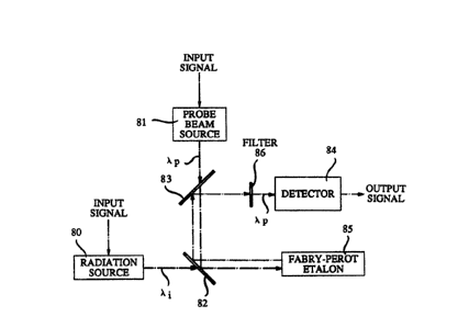
PIG. 8 schematically depicts elements of exemplary apparatus
according to the invention. The apparatus comprises a source 80 of "input"
35 radiation of wavelength Ri, a source 81 of "probe" radiation of wavelength ~p,
half-silvered mirrors 82 and 83, a FP-etalon according to the invention 85, a
1 3~7qq
- 11 -
filter 86 and a radiation detector 84. Exemplarily ~p and ~i are selected such that
the nonlinearity of the etalon is relatively small at ~p and large at ~j. Either one
of ~ and ~j can be identified with ~O~ If only probe radiation is directed at the
etalon then there is substantially no reflected radiation. If both probe radiation
S and input radiation are directed at the etalon the optical state of the etalon can
change such that a substantial amount of reflected probe radiation is present, and
can be detected by means of the detector, resulting in an output indicative of the
optical state of the etalon. For instance, if the etalon contains GaAs active
material, then ~j and ~p exemplarily are 868 and 873 nm, respectively. If other
10 active materials (e.g., InGaAsP and related compounds) are used then the
appropriate wavelengths would be different. If two or more input beams
(wavelength ~) can be dîrected onto the etalon, each of which can cause the
described change in the optical state, then the etalon functions as a logical ORgate. Other logic functions can, of course, also be implemented. Finally,
15 apparatus according to the invention typically comprises a multiplicity of
individually addressable devices, e.g., etalons comprising TLs.
Example 1~ By MBE was grown an approximately 1 ,um thick body
which contained 9 TL layers (about 10 nm thick InO 1 lGaO 89AS) spaced about
1~3 nm apart, the remainder of the body being GaAs. Alo 4Ga0 6As layers
20 (465 nm thick) were grown on both major faces of the body to prevent surface
recombination. The body was then sandwiched between diclectric mirrors to form
a Fabry-Perot etalon. The etalon showed about 80% recovery at 300 ps delay
after illumination with an 850 nm wavelength input beam. An otherwise identical
comparison device lacking the TLs showed no sign of recovery at 300 ps delay.
25 It is known that devices similar to the comparison device typically have about
5 ns recovery.
Example 2: A multiplicity of etalons is made substantially as
described in Example 2 of U. S. patent application Serial No. 870,842, except that
the spacer body contains 9 TLs, substantially as described in Example 1 above. A30 metal TL optionally can also serve as a mirror in a FP etalon, or electrical contact
can be made to the metal FP, e.g., to provide an electric field that can assist in
moving carriers from the first semiconductor material into a TL.