Note: Descriptions are shown in the official language in which they were submitted.
--~ 1 30~
-- 1 --
IMPROVED CIRCtlIT ARRANGEMENT FOR MICROCOMPUTER
BACKGRO~D OF THE INVENTION
Field of the Invention
The present invention relates generally to a
microcomputer and more specifically to a data bus
arrangement which improves the speed with which data
can be moved within the system. ?
BRIEF DESCRIPTION OF THE DRAWINGS
The various features merits and advantages
inherent to the instant invention will become more
clearly appreciated as a description of the preferred
- embodiments of the same prvceeds taken in conjunction~
with the appended drawings in which:
Fig. 1 is a block diagram depicting the
operations performed by a prior art arrangement
discussed in the opening paragraphs of the instant
disclosure;
Fig. 2 is a timing chart showing the stages
involved in moving data from a CPU to an external
memory;
Fig. 3 is a circuit diagram showing a prior
art circuit arrangement which has also been discussed
in the openging paragraphs of the instant disclosure;
Fig. 4 is circuit diagram showing the
arrangement which characterizes a first embodiment of
the instant invention;
Fig. 5 is a timing chart showing the various
signal which are produced and/or utilized during the
operation of the circuit shown in Fig. 4; and
Fig. 6 is a circuit diagram of second
embodiment of the present invention.
. . .
. : , ,
:
' . ' '
1 3()~1 4
Description of the Prior Art
Currently used microcomputers inevitably
include on a single silicon ship, a central processing
unit CPU, a read only memory ROM, a random access
memory RAM, an input output interface I/O, and a timer
or clock circuit.
The CPU of such devices includes a register,
an arithmetical unit (ALU) and an internal data bus
whic is used to transfer data between the two. These
devices further include an external data bus which is
used in conjunction with the internal bus to move data
to peripheral circuits.
Fig. 1 shows an example of how the currently
used (prior art) devices have managed the movement of
data.
Data from the internal register of the CPU
is inputted to the ALU and subsequently processed. The
result is latched in a temporary register. This data
is then transferred to the internal data bus, latched
in an output data latch and outputted therefrom to the
external data bus. The data appearing on the output
terminal of the chip is transferred into a memory
located externally of the chip on which the CPU and ALU
are formed.
Fig. 2 depicts the number of bus cycles
required to achieve the above mentioned data transfer.
In the first half of the first bus cycle (nth bus
cycle) data from the internal register is inputted to
the ALU. In the latter half of the same cycle, data is
- lA -
.
A
.
- . ,
~ .
1 3 0 ~
-- 2
processed and the same time the internal bus is pre-
charged. During the first half of the next cycle
(viz., the n+l cycle) the -temporary charge is stored by
temporarily latching the same. During the second half
of this cycle, data is outputted to the external bus,
and in the first half of the n+2 cycle, the data is
written into an external memory.
Thus, as will be clear, there is a full bus
cycle between the one in which data is inputted -to the
ALU and the one in which data from the CPU is actually
written into memory. In this case the the result from
the ALU is determined during the first half of the n+l
cycle but even though the processing is complete a
total of three full bus cycles are required to transfer
the data.
In addition to the above the currently used
.
devices have included circuit arrangements such as
shown in Fig. 3. In this figure, la deno-tes a ROM, 2a,
2b, 2c and 2d denote internal function registers which
act as a program counter, a common use register, a
stack pointer, an accumulator, and a program status
word, respectively. These internal function registers
2a - 2d are connected by way of an internal data bus 3,
a data buffer 4 and an external bus 5 to peripheral
function register 6.
The data contained in these internal
function registers 2a - 2d is -transferred to the
peripheral function register 6 through the above
mentioned internal bus 3, data buffer 4 and external
bus, while in the reverse instance the data in the
peripheral function register is supplied via the same
path.
However, with this type of arrangement the
rate at which the bus can actually move data is
insufficiently high to meet high speed processing
requireMents and hampers the attainment of currently
,, ~ .............................. ~
1 30~
3 --
required data speed handling and management targets.
SUMMARY OF THE INVENTION
It is an object of the present inven-tion to
provide a system which enables increased data transfer
speed using simple hardware arrangements.
In brief, to speed up data transfer one
embodiment of the invention features a -transmission
gate arrangement which pre- charges and transfers data
in internal and external buses with with the same
timing and which further in-tializes the internal bus
and a device such as an ALU, every bus cycle. A second
embodiment speeds the data transfer in -the buse~ per se
by providing two data transfer paths through the
interconnected buses and reducing the combined
resistances of the internal and ex-ternal buses in the
order of 50~.
More specifically, a first aspect of the
present invention comes in the form of a microcomputer
which comprises a CPU, said CPU including a calculation
unit and an internal bus; an external bus operatively
connected with said internal bus; and transmission gate
means for prP-charging and transferring data into said
internal bus and said external bus with the same
timing, and for initializing said calculation unit and
said internal bus on every bus cycle.
A second aspect of the invention comes in
the form of a microcomputer which features: a CPU, said
CPU inluding a first register and an internal bus, said
internal bus having first and second ends; an external
bus having first and second ends, said first end being
connected with the first end of said internal bus and
said second end~being connected with the second end of
said internaI bus; a second register operatively
connected with said external bus; and transmission gate
means for transferring data between said first and
second registers via said internal and external buses.
. .
1 3 0 (~
- 4
A further aspect of the invention comes in
the form of a microcomputer which features: a CPU, said
CPU including a ALU and an internal bus, said internal
bus having first and second ends; an external bus, said
external bus having first and second ends, the first
end of said external bus being connected to the first
end of said internal bus, and t:he second end of said
internal bus being connected to the second end of said
extenal bus; and transmission yate means for
pre-charging and transferring data into said internal
bus and said external bus with the same timing, and for
initializing said ALU and said internal bus on every
bus cycle.
.. j,,, . ~- ,
.
1 3 ~ 1 4
DESCRIPTION OF THE PREFERRED El~ODIMENTS
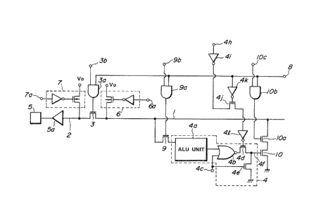
Fig. 4 shows a circuit arrangement which
characterizes a first embodiment of the present
invention. In this figure the CPU internal bus 1 and
the external data bus 2 are connected by a transmssion
gate formed of n-channel MOS-FET 3. This transmission
gate 3 is connected to the output of an AND circuit 3a.
One of the input terminals 3b of this AND circuit 3a is
supplied with a control signal Cl which is produced by
control circuit of the microcomputer which will be
described hereinlater with reference to Fig. 2C; while
the other input terminal is supplied with a bus cycle
pulse signal Q0 of the nature shown in Fig. 5A and
which is applied to the pulse cycle input terminal 8.
The external bus 2 is connected to a buffer
circuit 5a by way of output terminal 5. The internal
and external buses 1 and ~ are respectively connected ,
with precharge circuits 6 and 7 in a manner to bP
supplied with a precharge voltage VD. These precharge
circuits 6 and 7 have input terminals 6a and 7a
respectively which are supplied with control signals in
- form of a second bus cycle clock pulse signal Q2 of the
nature shown in Fig. 5B. When this signal assumes a
high level "1" the internal an~ external data b~ses 1
and 2 precharge and assume a high level by way of
example.
In the instant arrangement, the bus cycle
pulses Q0 and Q2 are arranged to have the same period
~viz, the same bus cycle time) and are arranged so
that, as shown in Fig. 5, when one assumes a high level
"1" the other assumes a low level "0" and vice versa.
The cGntrol signal Cl is arranged so that
during the n-lth cycle it assumes a high level at
timing coincident with the leading edge of the Q0
signal and remain at a high level until the next
A
1 3 0 ~
leading edge of said signal appears in the nth cycle.
Accordingly, signal Cl is such as to rise to a high
level in every other bus cycle.
The internal bus 1 is connected to the ALU
by way of a n- channel MOS-FET 9. In this instance the
internal bus is connec-tecl to the drain of the MOS-FET 9
while the source thereof is connected with the input
terminal of the ALU. The gate of the device is
connected to the ouput of an AND circuit 9a. On of the
input terminals (viz., terminal 9b) of this AND is
- arranged to receive a control signal C2 of the nature
shown in Fig. 5D. This signal is produced by the
control circuit of the microcomputer.
On the other hand, the other input terminal of the AND
circuit is arranged to receive the bus cycle clock
pulse signal Q0.
As shown in Fig. 5D the second control
signal C2 is arranged to assume a low level when the
signal Cl assumes a high level and vice versa.
Accordingly, the MOS-FET g is arranged to
assume an ON state when the bus cycle clock pulse
signal Q0 assumes a high level.
The ALU unit 4a is arranged so that output
terminal thereof is connected with one of the inputs of
a NOR circuit 4b. The other input terminal of the NOR
gate 4b is connected with a terminal 4c which is
supplied with the second bus cycle clock pulse signal
Q2. The output of the NOR gate 4b is connected with a
drain of n-channel MOS-FET 4d. The source of this
MOS-FET 9 is connected with the gate of a MOS-FET 10.
Further, in the instant arrangement, the source of the
MOS-FET 4d is connected with drain of a MOS-FET 4e
which form~ part of the initialization circuit.
The source of this MOS-FET 4e is grounded while the
gate thereof is connected with -terminal 4c.
The node 4f which de~ined between the ~
: '
. .. ~ .. . . . .
130881~
-- 7
MOS-FET 4d, 4ae and 10 is such as to develop a low
level "0" when the second bus cycle clock pulse signal
Q2 assumes a high level "1".
A terminal 4h associated with an inver-ter 4i
is supplied with fourth control signal C4. This signal
is identical to signal C2 as shown in Fig. 5D. This
signal is supplied by way of inverter ~i to the drain
of a n-channel MOS-FET 4j. The source of this MOS-F'ET
4j is connected by way of inverter 41 to -the gate of
MOS-FET ~d.
The first bus cycle clock signal input
terminal 8 is connected by way of inverter 4k to the
gate of the MOS-FET 4j.
Accordingly, with this arrangement the signal shown in
Fig. 5e is produced. As shown this signal is such as
to assume a high level in the n-lth cycle until the
occurrance of the trailing edge of signal Q0. The
- signal remins at low level "0" until such time as the
next trailing edge of signal Q0 occurs just prior the
end of the nth cycle. Following this, the signal
remains at a high level "1" until such time as the next
trailing edge of signal Q0 occurs in the n+l cycle.
The source of the MOS-FET 10 is yrounded
while the drain is connected to the source of n-channel
MOS-FET 10a. The drain of this MOS-FET 10a is
connected to internal bus 1 while the gate thereof is
connected with the output of an AND circuit 10b. One
input of this AND circuit 10b is connected with an
input terminal 10c which is adapted to receive a
control signal C3 of the nature shown in Fig. 5C. The
other input of the AND gate 10b is connected to
terminal ~ so as to receive the first bus cycle clock
signal Q0. With this arrangement when signal Q0
assumes a high level "1" MOS-FET 10a is induced to
assume an ON state.
As the remaining construction and
,
1 3 0 ~
8 --
arrangement of the circuit shown in Fig. 4 is
essentially the same as Eound in convential
arrangements, a detailed explantion of the same will be
omitted for brevity.
With the above described arrangement, during
the first half of the nth bus cycle when signal Q2
assumes a high level "1" MOS- FET 4e is rendered ON and
signal appearing on node 4f assumes a low level. This
causes the ALU to be initialized. Following this in
the last half of the nth cycle, while signal Q0 remains
at high level "1" -the MOS-FET input gate 9 is
maintained ON and during this period the data in the
internal register of the CPU (not sh~wn) is inputted to
the ALU. In addition to this the MOS- FET 4d is
conditioned to assume an ON state and the signal shown
in Fig. 5E rises to a high level "1" until -the leading
edge of signal Q2 is produced in the n~lth signal.
This maitains the signal in question at a high level
for a time To. In response to signal Q2 assuming a low
level "0" in the n+lth cycle the result produced by the
; ALU is subject to a timing latching at node-4f.
Next, during the period To in n+lth cycle
the MOS-FET 4d is ON, while the signal Q0 is at a high
level "1" the MOS-FET 10a is rendered ON, and the data
indicative of the result of the ALU processing is
transferred through the MOS-FET 10a, the internal bus
1, transmission gate 3, external bus 2 and buffer
circuit 5a to the output ~erminal 5.
While the bus cycle clock pulse signal Q2 is
at a high level "1" the node 4f is initialized via
discharge~. Viz., when the MOS-FET 4d transmission gate
is ON the signal appearing on node 4f becomes "0" with
the result that the adjacent MOS-FET 4d goes ON. This
induces the signal appearing at node 4f to either
~ 35 remain at low level "0" or change from "1" to "0". As
`~ a result,;the MOS-FET 10a is ON and data is transferred
:: :
: ;:
.
l 3 n ~ 4
-
to the data bus 1 before the outcome of the ALU
processing, so that it is not required to pre-charge
the internal da-ta bus 1.
Accordingly, during the above mentioned
n+lth bus cycle the data latched on node 4f is directly
transferred to the internal and external data buses 1
and 2 and driven to the outpu-t terminal 5, thus
rendering it possible to achieve the required da-ta
management in 2 data bus cycles. This of course reduces
the number of bus cycles required and enable the
desired tasks to be achieved in a shorter time.
Further, with -the instant arrangement as the internal
and external data buses are subject to the same timing,
and as data is being transferred it is not necessary to
perform individual data input and output latches
between the input and output buses, and it is possible
to omit the pre-charging operations. This permits an
advantageous simiplication in hardware.
Fig. 6 shows a second embodiment of the
present invention.
In this figure for the sake of clarity only a single
register 2' is illustrated. However, it is to be
understood that this single unit is representative of
devices such as a program counter, stack pointer,
accumlator, program password type registers.
As shown, the internal register is connected
with an internal data bus 3'and with the gate of a ;
MOS-FET 9'. The source of~this MOS-FET 9' is connected
to the source of another MOS-FET 9a'. The drain of the
latter mentioned MOS-FET is connected to the internal~
data bus 31 while the gate of the same is connected
with~a ROM in a manner to be supplied wi-th a
predetermined contrl single. Viz., when MOS-FET 9a is
ON the data in the internal register 2' is supplied to
the internal data bus 3'. In this figure terminal 2i'
is arranged to function to receive a signal which
: ~ :
...... . , ,. ~ - .
,
'
':
l3n,~l4
- 10 -
indicates -that data is to be wri-tten into the internal
register 2'. In this arrangement the input terminal
2i' is operatively connected wih the ROM la' in a
manner to receive said prede-termined signal.
In the instant arrangement the internal data
bus 3' is provided with two transmission gates 7' and
8'. Both are formed of n-channel MOS-FET. The drain
of gate 7' and the source of gate 8 are connected to
the "outboard portions" of the internal bus 3' while
the source of gate 7' is connec-ted to the drain of gate
8' through the portion of the bus extending
therebetween. A peripheral function register 6' is
connected in parallel with an external bus 5' in manner
to be operatively connected with the gates 7l and 8' in
the illustrated manner.
The peripheral function register 6' is
provided with a terminal 6a' which is adapted to
receive a read control signal from the ROM. This
device is also provided with a terminal 6b' is adapted
to recieve a read out control signal.
It will be noted that in this drawing the
internal and external data buses are illustrated by a
single line, however this is only for the sake of
illustration. In an 8 bit type one chip
microprocessor, these buses wouId in fact include 8
lines (16 lines in the case of a I6 bit machine etc.)
In the instant arrangement in the case data
is transferred~from the internal register 2' to the
peripheral function register 6' ~the internal and
external buses being previously precharged) the control
ROM la' outputs a controI signal to the gate of the
MOS-FET 9a' which renders the same ON. Data from the
internal function register 2' is transferred to the
internal bus 3' via the gates 7' and 8' which are also
rendered ON. From the internal bus 3' the date enters
the external bus 5' and is transferred into the
, .
, '
l 3n~ 4
peripheral func-tion register in the presence of a
control signal from the control ROM la' appearing on
the terminal 6a'. In this case data from the internal
register 2' is supplied to the internal and external
buses via two separate directions.
Given, that -the resistances of the two paths
are Rl and R2 respective]y, the resistance developed
between the internal and peripheral registers 2' and 6'
can be represented as fol.lows:
R = Rl ~ R2/Rl + R2 ....... (1)
Assuming that Rl = R2 for the sake of
explanation, it can be seen that the resistance of the
arrangement shown in Fig. 6 is half that of an
arrangement wherein da-ta is transferred in one
direction only. The same effec-t exists in -the case
data is transferred from the peripheral register 6' to
the internal one 2'.
As will be appreciated this marked reduction
in resistance enables data to be physically tansferred
with less resitance and therefore faster. The
arrangement of the second embodiment of the present
invention therefore enables data to be moved faster
which in combination with the first emodiment which
reduces the number of bus cycles necessary for any
given data transfer. The combined effect is highly
advantageous in promoting high speed processing by
speeding up the rate wi-th which data can be moved
within the system.
' ' ,
-