Note: Descriptions are shown in the official language in which they were submitted.
` 1309173
AV-3~57
CHROMA PHASE WORD ENCODE/DECODE
IN A VIDEO PROCESSING SYSTEM
BACKGROUND AND S~MMARY ~F THE INVENTION
This invention relates to a circuit for
enabling the correction of the phase of a color signal
in a video processing system, and particularly relates to a
circuit and method for inserting chroma phase informa-
~ion in a video data path and for subsequently recover-
ing the chroma phase information downstream.
Presently known video signal processing
systems generally employ a main memory for storing
video signals and a timing correction circuit for
correcting the time base or frequensy errors that occur
during the processing of the video signal. Such errors
in timing or frequency degrade the video signal and the
resultant television image
Another problem that is experienced with
video signal processing systems that incorporate
relatively complex circuitry is color instability that
adversely afects the color representation of the
television image.
In the United States, television signal
processing systems employ a standard NTSC format
wherein each successive horizontal line is charac-
terized by suhcarrier signals of opposite phase, so
that there are two different line types when using such
a format. With the NTSC system, it is necessary that
the chroma signal appearing at the output of the video-
tape recorder be coincident with the phase of the
station reference signal, in order to ensure the
correct color of the televis1on picture. The tele-
vision reçording systems employ a time base correction
network,which includes a chroma processor for correct-
ing colorand adropout compensator to compensate for
missing video signals. The time base correction system
~ .
1 3 0 9 1 7 3
requires the identification of the incoming subcarrier
phase as well as the output subcarrier phase,which then
are compared in order to provide proper color correc-
tion and the correct color in the resultant television
picture.
In countries that use a PAL standard format
which employs horizontal lines of four different
subcarrier phases resulting in four different line
types, identification of each of the line types is
necessary for proper color correction.
In prior art systems, circuits for
identifying the chroma line type are generally located
in a stage or stages preceding the main memory and the
time base corrector (TBC) circuit. However, it has
been found that with recently developed TBC systems,
which are substantial improvements over prior art
systems, color correction effectively is accomplished
when processing the video signal utilizing the chroma
line type information after time base correction is
achieved. It would be desirable to accomplish ~he
chroma phase correction after time base correction and
with minimal circuitry.
The present invention overcomes the various
disadvantages of previous mention in a time base
correction system which includes chroma phase correc-
tion,wherein color picture stabilization is achieved
after the time base correction error has been removed.
To this end, the invention provides means for carrying
-the required line type identifying signals through the main
timebase correction process of the main memory for use on
the reference side of the TBC, utilizing a minimal
amount of circuitry while eliminating the need for the
overhead of additional data bits.
In a televisîon VTR playback system made in
; 35 accordance with this invention, color correction is
achieved by encoding chroma phase as line type information
in the form of a digital word at the beginning of
the active picture period of each horizontal line of
''
`
.,
.,,
:'
;'
`` 1 309 1 73 A~ 3257
incoming video data, and prior to the timebase processing
of the video data via the main memory. The chroma line type
identified by the digital word is passed to the output
of the memory and is extracted to identify each line,
whereby phase correction of the chroma signal is accom-
plished after time base correction in the same channel.
BRIEF DESCRIPTION OF q'HE DRAWINGS
The invention is described in greater detail
with reference to the drawing in which:
FIGURE 1 is a block diagram of the circuit
for inserting digital chroma phase information in the
video data.
FIGURES 2A-D are waveforms showing the
relationship between the horizontal sync and burst of the video
signal and the horizontal signals derived from the
recorded tape.
FIGURE 3 is a schematic diagram of an
implementation of the multiplexing means of FIGURE 1.
FIGURE 4 is a schematic diagram of an
implementation of the line type control circuitry
integral with the multiplexing means and the comparator
of FIGURE 1.
DESCRIPTION OF THE PREFERRED EMBODIMENT
In NTSC and PAL television systems, the
chroma signal differs in phase successively for each
horizontal line. The horizontal lines of the NTSC
system appear in a sequence of four different fields
consisting of two different types of lines, whereas the
PAL system employs an eight field sequence with four
different types of lines~ Since chroma signal phase
correction is required downstream of the main memory,
chroma line type references also are needed for
identifying the line type in order to be able to
process the color signal properly~ The line type
signals, designated aenerally as H/2 and H/4 identification
signals (FIGURES 2C, 2D) represent respectively one
:
,, . ~ ;
1 309 1 73
-4- AV-3257
half and one-quarter of the horizontal synchronizing pulse
frequency, and may be used in NTSC and PAL format TV
systems. Although the following description primarily
is directed to the use of H/2 identification signals as
used in an NTSC system, the circuit of this invention
is also applicable to the PAL system in which H/4 and
H/2 identification signals are used.
Further, when a helical scan VTR is operated
to create special effects upon the playback o recorded
video information, such as slow motionl fast motion, or
still frame, or is operated to reproduce recorded video
for display as the tape is shuttled at high speed, the
speed of transport of the tape is varied during
reproduction of the recorded video information and the
~5 position of a movable playback head is controlled to
maintain it registered with the recorded tracks of
video information being reproduced. Thus for special
effects and shuttle modes of a VTR, it often is
necessary to repeat or skip recorded tracks of
television fields. The invention line type insertion
techni~ue provides the proper line type identification
at the reerence side of the memory regardless of the
mode of operation.
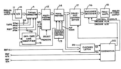
With reference to FIGURE 1, an analog video
input signal (FIGURE 2A) is obtained from a recorded
tape at terminal 11. The off-tape video data signal is
converted in an analog-to-digital converter 10 to
digital form and is applied to a ~iming correction
circuit 9 and thence to a multiplexing means 12. The
timing correction circuit 9 may comprise four one line
memories which basically are controlled by tape 2Fsc and
4Fsc clocks on lines 24 and reference 2Fs and 4Fsc
clocks on lines 26. The video data signal is written
into the timing corrector circuit 9 via the tape 2Fsc
and 4Fsc clocks in blocks of selected number of samples
corresponding to a horizontal line. Since the data is
written into the circuit 9 at the tape rate, with
timing derived from the color synchronizing o~rst that
~ .
~.,
~309~73
occurs at the beginning of each horizontal line interval of
the composite color television signal, the data is not
corrected for color subcarrier phase errors as well as other
timing errors. To eliminate the subcarrier phase errors, the
data stored in the timing correction circuit 9 are read at a
time determined by the fixed or stable frequency and phase
reference 2Fsc and 4Fsc clocks. Thus the circuit 9 serves to
r~-time the video signal data obtained therefrom in
accordance with thP re~erence clock signals, and to supply
the data to the main memory in one line blocks for subsequent
time base correction.
The re-timed video signal is supplied to the
multiplexing means 12 which also receives chroma line type
identification signals MEM CON TAPE H/2, H/4, derived as in
FIGURE 4 from the tape H/2, H/4 signals extracted from the
incoming video signal, to serve as off-tape timing signals.
The MEM CON H/2, H/4 signals thus are related to the tape
H/2, H/4 si~nals respectively, and are dif~erent, for
example, only when the system is in the shuttle or slow
motion modes of operation, when data is written into the
timing correction cixcuit 9 at a different rate than data is
written inta the main memory 14. The multiplexer 12 responds
to a SELECT command (further descr.ibed in FIGURE 3 as INSERT
WORD and DROPOUT signals) for accepting the MEM CON TAPE H/2
and H/4 identification signals from a line identifier 13,
where~y the multiplexer switches from the active picture to
the corresponding-digital chroma line type word
repre~entative of the tape line type.
More particularly, FIGURE 3 illustrates a schematic
rn/C~
.~
,
''
1 30q 1 73
5a
of the multiplexing means 12 used for line type insertion as
well as dropout insertion when a dropout occurs. After the
re-timed video data ~amples are supplied from the timing
correction circuit g in the form of 9-bit words, they are
rephased by clocking them through buffers 28, 30 with
reference clock signals 2Fsc and 4Fsc. Connected to the
video bus in parallel with the outputs of the buffers 28, 30
are buffers 32, 34 comprising a line type insertion circuit.
Additionally, connec~ed in parallel with the outputs of the
first two circuits are buffers 36, 38 comprising a dropout
insertion circuit. The video data are multiplexed into two
channels to reduce the speed requirements of the buffers 32-
38.
These three circuits are connected in parallel to
the video data bus at this point so that a choice may be made
whether to insert, for a particular sample period of the 2Fsc
reference video bus clock, either the
rn/
-6- 1 309 1 73 AV-3257
sample value output from the line memory in timing
correction circuit 9, a sample value indicative of the
line type, or a sample value indicative of the presence
of a dropout. The selection of which value is inserted
in a particular sample location is made by a logic
circuit 40 from input signals INSERT WORD and DROPOUT
which comprise the SELECT signal of FIGURE 1. The
selection is accomplished by enabling one of the
circuits to allow passage of the sample onto the video
bus while the other two circuit outputs are tristated.
The signal INSER~ WORD is output from a read
address counter (not shown) of the timing correction
circuit 9 which indicates ~hat the end of a horizontal
line has occurred, and thus that horizontal blanking o~ the
next line is to begin. The read address counter in essence
counts the number of samples per active picture line,
which number is preloaded and reflects the NTSC, PAL,
color standard, and ~hen generates a carry signal which
indicates the beginning of the horizontal blanking
interval. A low logic level of the INSERT WORD signal
selects or e~.ables the outputs of the buffers 32, 34 to
insert on the video bus in that sample period the value
of the logic levels on their inputs. The values which
are inserted are the type of the horizontal line which
will next be read out of the line memory in the circuit
9. This in~ormation is initiated by a system/memory control
module as depicted at 15, FIGURE l, and is supplied as the
signals MEM CON H/2, H/~ to the line type insertion circuit
by the line identifier 13. The signals are transferred to
the video bus at the correct time corresponding to the time
of the INSERT WORD.
The buffers 36, 38 of the dropout insertion
circuit are enable by the low logic level output of a
NAND gate 42. When the buffers 36, 38 are enable~ they
insert a word of all zeros (low logic level~ on the
; video bus to indicate the sample is a dropout. The
output of NAND gate 42 enables this function when the
DROPOUT signal is clocked through a bistable 44 at a
2Fsc rate. The dropout interval is previously detected
7- 1 309 1 73 AV-3257
as video samples having a dropout condition and is
detected by an upstream detector and transferred
through the timing correction circuit 9 coincident with
that particular period. Thus, the dropout insertion
circuit exchanges a dropout value for the sample value
which was previously stored during the dropout
interval. The gate 42 is enabled for the insertion of
the word at the time of the DROPOUT signal unless the
INSERT WORD signal is present.
The buffers 28, 30 allow the data samples to
be clocked through them when the output of a NAND gate
46 is a low logic level, thereby enabling the inverted
OE inputs of the devices. The buffers 28, 30 are
enabled if neither the INSERT WORD signal nor the
DROPOUT signal is present. Otherwise, the NAND gate 46
disables the buffers 28, 30.
Therefore, a priority method for the
insertion of the sample values on the video data bus is
implemented in this manner. The INSERT WORD signal
indicating the end of the active video has first
priority and causes line type identification to be
inserted in the data stream. The DROPOUT signal has
second priority and, in the absence of the INSERT WORD
signal, causes dropout identification samples to be
inserted in the data stream. Otherwise, which is
usually the case, the absence of the INSERT WORD and
DROPOUT signals allow the data samples to be passed
through the multiplexing means 12 as the data stream.
The digital video data signal, including the
digital word indicative of chroma line type
information, is applied to a main memory 14. The
memory stores the digital video signal and the digital
words of the chroma phase information (and the dropout
word if a dropout occurs3 in blocks of one line of
video data. The memory control circuit 15 controls the
read/write main memory, and includes a timing generator
that produces read and write sync pulses for
controlling the timing and location of storage of each
.
-8- l 309 1 73 AV-3257
video line, including the chroma p~ase samples. The systemt
memory control circuit 15 provides row/column addresses
and various row/column strobes and control signals for
the write and read processes for passing the video data
signals and the line type information (and the dropout
word if present) through the memory 14. The write and
read processes are timed whereby mis-positioning of the
horizontal and vertical phase is corrected at the
output of the main memory 14 to provide a time base
corrected signal synchronous with reference signals.
In accordance with the invention, the
resulting video signal which has been time base
corrected is strobed into a clocked latch 20,that
strips two bits from the stored line type word which is
read from the main memory 14 as 9-bit words. One of the bits
is used in the NTSC standard to identify the two different
chroma line types, while both bits are used in the PAL
standard to identify the four chroma line types
thereof. The clocked latch 20 receives a reference
horizontal sync pulse H to enable loading samples of
the chroma phase word for each horizontal line. The
clocked latch 20 supplies a MEM OUT H/2 (NTSC)
and MEM OUT H/4 (PAI.) identification signal to
a comparator 22 which also receives stable
reference H/2, ~/4 signals from, for example, a sync
generator (not shown) of the TBC. If the logic levels
of the MEM OUT signals differ from the reference signals,
then the difference is detected by the comparator
22 and a control signal DECODE H/2 is supplied to an
encoder/decoder 16 of a color processor circuit. In
the PAL standard both the DECODE H/2 and a DECODE H/4
control signals are supplied to the encoder/decoder 16.
The encoder~decoder responds to the control signal and
separates the chroma from the luminance signal,and then
inverts the phase of the chroma signal via a chroma
inverter of generally known ~onfiguration~to matrh the
phase of the chroma signal to that of the reference
signal. The video data signal including the inverted
'~
1 309 1 73 AV-3257
chroma signal are added to the luminance signal and
passed to a processing amplifier 18. As an alternative
approach, the video data is delayed and shifted by
one-half of the color subcarrier cycle or by 180 to
match the phase of the station reference signal before
being passed to the processing amplifier 18.
The comparator 22 also supplies the DECODE
H/2 control signal to the dropout compensator 17 to
identify the V-axis switch sense in the PAL standard
which is required for dropout compensation. In
response to a selected logic level, the compensator 17
determines the reference phase of a PAL modifier
7 circuit which modifies the chroma signal of an adjacent
line of video to supply the same chroma phase as the
line having the dropout.
FIGURE 4 is a schematic of line type control
` circuitry for receiving the line type information
indicative of an incoming tape field sequence from
signals TAPE H/2 and TAPE H/4, and the line type infor-
mation indicative of the desired output reference field
sequence from reference signals REF H/2 and REF H/4.
The circuitry in turn supplies signals to different
components in the TBC to control line type and field
sequencing operations in accordance with the invention.
In general, the line type control circuitry
` 25 comprises two sections; a control signal generation
section and a line type data generation section. The
control signal generation section is controlled by a
PROM 50, and the data generation section is controlled
by a PROM 80. A data latch 52 is connected to the
write portion of the memory control data bus and provides
means for an integral microprocessor (not shown~ to write
a data word comprising an address, into the PROM 50 via a
select line Sl9. The data outputs D~-D4 of the latch 52 are
used by the PROM 50 to select particular sections or address
blocks of the memory for decoding inputs A~-A3. Further, the
data lines D0-D4 include a bit which either enables or
.~
..
1 3 0 9 1 7 3
disables the PROM by applying a logic level to its G2
input.
In this way the microprocessor chooses
certain decoding sections of the PROM 50 to change the
decoding algorit~n ~ased on TV st~ndard. The TV
standard is set by the operator and decoded by the
system/memory control circuit 15.
Similarly, the PROM 80 has data lines D5-D7 from the
latch 52 connected to its address inputs A5-A7. These
address inputs select certain decoding blocks in the PROM
80 for decoding data inputs to its other address lines
A0-A3.
The data generation section of the line type
control circuitry includes two D-type bistables 88 and
86, which receive a tape writé pulse representing
the start of a horizontal line, and which produce
a clocking pulse which is synchronous with the 2Fsc
clock. The pulse from the Q output of the bistable 86
clocks line type signals, ~APE H~2, TAPE H/4 of the
incoming data into bistable devices 54 and 84. This
line type information is then clocked into a latch 82
by a write enable signal at reference horizontal rate.
Outputs Q~ and Q1 of the latch 82 are connected to two
other D inputs of the latch 82. Therefore Q0 and Ql
represent the tape H/2 and H/4 signals at the beginning
of the pre$ent reference horizontal period, while Q2
and Q3 represent the tape H/2 and tape H/4 as they were
one reference horizontal period aqo. Both pairs of
outputs from latch 82 are supplied as four bits of an
address for PROM 80. The PROM 80 produces the two
signals MEM CON H/2, H/4, and are output to the
multiplexing means 12 from the Q0, Ql outputs of
the PROM 80 after being reclocked in a buffer 78 to be
synchronous with the 2Fsc clock pulse. Thus the PROM
80 designates the lines which are to be written into
the main memory 14.
The multiplexing means 12 . uses these
two signals as the two most significant bits of the
read address in the line memory integral therein and
. ,40 also inserts these coded signals into the data stream
prior to the data of the horizontal line addressed by
~ t 3~9 1 73 AV-3257
these bits. In this manner, every horizontal line is
preceded by the information as to its type, as it is
clocked through the main memory 14 as previously
described. These signals are extracted from the data
stream after passage through the main memory to become
the MEM OUT H/2, H/4 signals which represent available
line type to the Al and A4 address inputs of the line
type comparator PROM 50. In combination with the
desired line type signals REF ~/2, H/4 which are input
to the A0 and A2 inputs of the PROM 50, these signals
are compared and provide enabling signals to the
control portion of the line type control circuitry.
The reference signals REF H/2, H/4 indicate the desired
output sequence of fields after being decoded by the
PROM 50 for TV standard,and the MEM OUT H/2, H/4
signals indicate the actual line type output from the
main memory 14 after being decoded by the PROM 50 for
the TV standard. Therefore, signals Q0-Q5 of the PROM
50 indicate certain control actions which must be taken
if the actual line type is to be changed to the desired
line type such that appropriate field sequence or color
correction can occur.
; The outputs Q0-Q5 of the PROM 50 are dis-
tributed to the D inputs of the bistables 45, 56, 60,
70, 72, and 74, respectively. These control si~nals
are clocked at the particular times to become control
signals to different parts of the TBC. For example,
the Q~ output is clocked into bistable 45 by the output
of a NAND gate 44 to become the lH shift signal output
from a NAND gate 48. The clock signal from the NAND
gate 44 is produced at the system reference vertical
REF V, if the color processor encoder/decoder 16 is not
present or disabled as indicated by the signal OP PRES.
This clocks the line type comparator PROM 50 output Q0
into bistable 45 at a vertical rate if the color
processor is not present or disabled and will add 1
horizontal line delay to the data path of the video
data required for color correction mode by memory
-1~- 1 309 1 73~v-~
co~trol in PAL and PAL-M, when a 90 subcarrier phase
is needed, which may be accomplished by that delay. If
the color processor encoder/decoder 16 is present and
enabled, the vertical timing control for color
; correction should not be used. This output is the
signal generated by the NAND gate 48~_lH shift to the
vertical timing control. The NAND gate 48 is enabled
by the microprocessor set line type correction on/off
signal.
The bistable 56 is cloc~ed by the output of a
NAND gate 76 to produce the signal 180 SHIFT at the
output of the NAND gate 58. The D input of the
bistable 56 receives the Ql output of the PROM 50 which
is an indication that color correction requires 180
degrees shift of color subcarrier phase. The 180
SHIFT signal is generated if the line type correction
on/off signal is a high logic level enabling the gate
58. The clocking signal to bistable 56 is timed to the
reference horizontal sync signal delayed by three
subcarrier cycles. This signal is transmitted through
the gate 76 which is enabled by the color processor
encoder/decoder 16 being present. Likewisej bistables
60, 70, 72, and 74 are clocked by the output of the
NAND gate 76.
The outputs of the bistables 60 and 70
produce color processor color correction control
- signals DECODE H/2, H/4 if NAND gates 62, 66,
respectively, are enahled by the line type correction
on/off si~nal. If I10 line type correction is to be
applied, then the DECODE H/2, H/4 signals are taken
directly from the MEM OUT H/2, H/4 signals by exclusive
OR gates 64 and 68, respectively. If the line type
needs to be corrected, ~he MEM OUT H~2, H/4 are
inverted by the gates 64 and 68. The color processor
takes these decoding signals and produces color
correction from the input data of the main memory 14
; before providing the data to the processor amplifier
~ 18. The bistables 72 and 74 produce data shift signals
:
: .
-13- ~ 3 0 9 1 7 3 AV-3257
for the processing amplifier 18 data shift 180, data
shift 90 through respeetive inverters 73 and 75 if the
color processor encoder/decoder 16 is present~ The Q4
and Q5 outputs, respectively, decode into the type of
delay that the color processor will produce in the data
S going into the video bus path for the line type and
color sequencing data from the PROM 50.
The processing amplifier 18 reeeives the
video from the encoder/decoder 16 and diseards the syne
and burst portion of the ineoming signal and replaces
these signal components with new sync and burst derived
from the syne generator. The aetive pieture is added
to the new sync and burst with a color corrected ehroma
phase whieh matches the new burst. The combined signal
is passed through a D/A converter and low pass filtered
to form the output eomposite video signal correctly
timed to the station referenee.
~,