Note: Descriptions are shown in the official language in which they were submitted.
1 3094~5
83-458
PATEN'rS
--1--
FIELD OF TBE INVENTION
This invention relates generally to the field of cathode
ray tube video display terminals, and more partlcularly, to a
video circuit enclosure for attaching a video circuit to the
cathode ray tube.
E~ACRGROUND OF THE INVENTION
Video displays are almost always provided at data
processing system work stations in order to provide a visual
representation of the information being processed at any given
instant. Most video displays have a cathode ray tube (CRT) to
generate images of the information they are designed to
display. Cathode ray tubes are large vacuum tubes that have a
flat surface at one end that serves as a screen face, and
taper into a cylindrical neck at the opposite end. A
phosphorous coating is applied to the inside of the screen
face, and an electron-emitting source, an electron gun, is
housed in the neck of the tube and pointed toward the screen
face. The electron gun is triggered to selectively emit
electrons by a video drive circuit located external to the
~RT. The electrons strike the phosphorous on the screen face,
- 1 309~85
~3-458
PATENTS
2--
and excite it so light is momentarily emitted. The light
emitted by the CRT is the visual image generated by the video
display.
Recent advances in CRT technology and video drive circuit
technology have made the development of ultra high resolution
video display terminals possible. These terminals are able to
generate images with exceedingly fine detail and shading that
was previously difficult to display. Moreover, many vidso
terminals currently being produced are able to generate color
displays. The ultra high resolution CRTs are able to blend
the three primary colors, which is typically what the electron
gun, or set of guns inside the CRT, generate, into a very
large spectrum of intermediate colors for display.
The new ultra high resolution video display terminals
have become very useful because they can produce very
complicated representations of the information being processed
by the data processing system. Moreover, these v-deo displays
can be incorporated into a desk-top publishing system that,
with the use of an appropriate printer, can be used to
generate quantities of documents that include both textual and
image material. An ultra high resolution display is an
integral part of a desk-top publishing system because it can
` 1 30~4~5
83-45B
PATENTS
--3--
be used to display what material will be printed before the
actual printing process is performed.
To date, however, there have been problems associated
with connecting the cathode ray tube of ultra high resolution
video display terminals to their associated video amplifier
circuits. The video amplifier circuit of a video display
terminal supplies the necessary signal voltages to the CRT to
drive the electron gun or guns therein. In the past, video
amplifier circuits have been on a circuit board, called the
"video board", that is attached to the CRT. Conductive leads
connected between the video board to a socket coupled to
contact pins on the CRT would serve as the paths for signals
transmitted to the CRT. In some instances, ~he socket was
mounted directly to the video board, and in other instances, a
hole was formed in the video board and the video board
disposed around the end of the C~T.
Problems have arisen because ultra high resolution CRTs
require CRT drive signals that are at very high frequencies in
order to generate the desired detailed images. As the high
frequency signals are forwarded to the CRT, the CRT inherently
acts as a capacitor, and the conductive path to it inherently
acts as an inductor. This results in the filtering and
1 3 0 9 4 8 5 PATENTS
--4--
distortion of signals forwarded to the CRT, consequently the
images generated by the CRT are subject to degradation.
Another problem associated with ultra high resolution
video displays is that the video amplifier opecates at a
relatively high power level and transmits voltages to the C~T
at very high frequencies. Consequently, the video amplifier
in effect is a generator of spurious electromagnetic waves
that could effect the operation of other nearby electronic
devices. This is especially true if the video display
terminal is adjacent other data processing devices that also
operate at relatively high speeds and hence may be effected by
even minute inductive currents generated by stray
electromagnetic waves.
Another consideration in the design of an ultra high
resolution video display terminal is the heat generated by
their video amplifiers. Ultra high resolution video display
video amplifiers generate large amounts of heat as a
consequence of the large amounts of power they consume in
order to provide the necessary video drive signals to the CRT.
If the heat generated by the video amplifier circuit is not
dissipated therefrom, the components that comprise the circuit
may overheat resulting in their malfunction or possible burn-
out.
- 1 3094~5
83-458
PATENTS
--5--
SUMMARY OF THE INVENTION
This invention provides a novel video circuit enclosure
for connecting the video board of a video display terminal to
the terminal cathode ray tube.
The video circuit enclosure of this invention includes a
shielded video box which is secured to the chassis of the
video display terminal it is part of. A video board, which
carries the video amplifier circuit, is secured inside the
video box. A heat sink is mounted to the video box and a
thermal path is established between it and the heat generating
components on the video board. A socket board, with a socket
for receiving the cathode ray tube contact pins, is disposed
inside the video box so that it is adjacent to the video
board. Attached to the socket board is a shielded video cover
that is disposed over the outside face of the video box. An
opening is formed in the video cover so the neck of the
cathode ray tube, with the contact pins, may be inserted
therein for coupling to the socket board socket.
A set of spring loaded contact pins are used to provide a
low impedance conductive path between the socket board and the
video board. The pins are soldered into the socket board and
1 3094~5
6 69904-lq3
the plns themselve~ abut surface contact pads on th~ vldeo board.
Compressible, conductive sprlng shlelds are dlsposed on the vldeo
box 80 that they are ln contact wlth the video cover to provide a
conductlve path therebetween.
When a video display termlnal wlth thls video circult
enclosure ls assembled, the cathode ray tube 1B mounted to a
bevelled frame so the socket board attached to lt ls dl6posed
inslde the vldeo box ad~acent to the vldeo board, and the vldeo
cover is urged towards the open face of the video box. The socket
board ls dl~posed inslde the vldeo box whereby the conductive plns
abut agalnst the contact pads on the vldeo board. The vldeo cover
ls disposed agalnst the video box whereby the sprlng shield~
provlde a conductive path therebetween.
The vldeo clrcult enclosure of thls lnventlon provldes
shleldlng for the vldeo ampllfler circult thereln located on the
vldeo board and the socket board thereln. Thls minlmlze6 the
posslblllty that electromagnetlc radlatlon wlll be radlated due to
the generatlon of video slgnals and thelr transmlsslon to the
cathode ray tube. Moreover, the distance the signals have to
travel between the video amplifier circuit and the CRT ls minimal.
Since the path the signals have to travel ls mlnlmal, so ls the
lnductance and consequentlal fllterlng of the high frequency
slgnals that result ln degradatlon of the deslred lmage.
The heat slnk attached to the vldeo box provldes an
efflclent means to dlsslpate the heat generated by the vldeo
ampllfler circult. Thls lnsureB that the vldeo ampllfler
components will not become overheated and subsequently malfunctlon
or burn-out.
1 309485
7 69904-143
Another advanta~e of this vldeo enclosure 18 that the
cathode ray tube and the socket board are not rigidly connected to
the vldeo board or the vldeo box. This ln~ures that lf the vldeo
display is ~olted, or otherwlse sub~ect to abrupt mechanlcal
shock, the cathode ray tube and socket board will be able to move
independently of the vldeo board. Thls elimlnates the posslblllty
of breaklng the connection to the CRT when all the components
attached to lt don't move together. Furthermore, only a mlnimal
amount of welght ls attached to the CRT. This minlmlzes the
possiblllty of lt breaking lf lt ls sub~ect to a mechanical shock.
The lnventlon may be summarlzed, according to a first
broad aspect, as a video clrcuit enclosure for attachment to a
cathode ray tube, the cathode ray tube havlng a screen face and a
neck extending away from the face, said neck hav~ng at least one
conductive terminal for the cathode ray tube, the video clrcult
enclosure comprising:
(a) video box formed of conductive materlal so as to form a
shield, said box disposed over the portion of the cathode ray tube
have the conductive terminals, said box formlng an open face into
which the cathode ray tube neck ls in~erted;
(b) a video board secured lnside said video box, said video
board including at least a video circuit for supplylng signals to
the cathode ray tube;
(c) a socket board dlsposed inslde sald vldeo box closely
spaced from said video board, said socket board having a socket
means for coupling to the cathode ray tube so that it is attached
thereto and in electrical contact with the cathode ray tube
termlnal;
1 309485
,. .
7a 69904-143
~d) an electrlcal connectlon means connected to ~ald ~ocket
- means able to maintaln a conductlve path for slgnal transfer
therebetween when sald vldeo board and sald ~oaket board move
relatlve to each other~ and
(e~ a vldeo cover formed of conductlve material dlsposed
over said vldeo box open face and formlng a hole ln whlch the
cathode ray tube 1B positioned, sald vldeo cover attached to sald
socket board and paced away therefrom BO that when sald ~ocket
board 18 dl~posed ln said vldeo box, sald vldeo cover ls ln
electrlcal contact wlth sald vldeo box.
According to another broad aspect, the present inventlon
provides a video circult enclosure for attachment to a cathode ray
tube, the cathode ray tube havlng a screen face and a neck
extending away from the face, said neck havinq at least one
conductive terminal for the cathode ray tube, the video circuit
enclosure comprising.
~ a) a video box formed of conductlve materlal BO as to form
a shield, sald box disposed over the portion of the cathode ray
tube having the conductive terminals, said box forming an open
face into which the cathode ray tube neck i8 inserted;
(b) a video board æecured lnslde sald video box, said video
board including at least a vldeo circuit for supplying slgnals to
the cathode ray tube;
(c) a socket board dlspo~ed lnslde said vldeo box and spaced
away from sald video board, said socket board having means for
recelvlng the cathode ray tube conductive termlnalB BO as to
secure the socket board thereto, and havlng a contact pin assembly
wlth at least one movable contact pln electrlcally connected to
1 309485
.
7b 69904-143
one of sald cathode ray tube conduative termlnal~, ~aid contact
pin belng biased toward~ sald video board~ and
(d) a conductlve contact pad located on ~ald vldeo board
ad~acent ~ald contact pin ~o that sald contact pln abuts thoreto
~o a~ to provlde a conductlve path between sald video board and
the cathode ray tube conductlve termlnal~.
- 1 30~85
~3-458
PATENTS
--8--
BRIEF DESCRIPTION OF T~E DRAWINGS
Figure 1 is a cross section view of the vldeo display
terminal with a cathode ray tube coupled into a video circuit
enclosure of this invention.
Figure 2 is a cut-away view of a video display terminal
with a cathode ray tube coupled into a video circuit Qf the
invention.
Figure 3 is an exploded view of the elements of the video
circuit enclosure of this invention.
Figure 4 i5 a detailed cross-sectional view of the spring
loaded pins used to provide conductive paths between the
socket board and video board of the video circuit enclosure of
this invention.
DETAILED DESCRIPTION OF T~E INVENTION
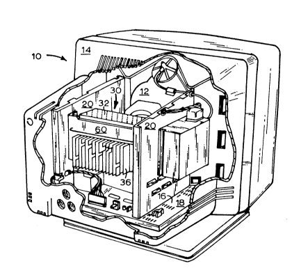
Figures 1 and 2 illustrate a video display terminal 10
which uses a cathode ray tube (CRT) 12 to generate visual
images of information being processed by the data processing
system (not illustrated) the video display terminal 10 is
attached to. The CRT 12, as well as all other components of
the video display terminal 10, is contained within a
protective housing 14 formed of a sturdy plastic. The CRT 12
1 ~()9485
9 69904-143
ls mounted on a chassls 16 whlch lncludes a horizontal base plate
18 that serves as a base for most of the video dlsplay 10
components, and two spaced-apart chassls walls 20. The CRT 12 is
mounted to a bevelled frame 22 that i~ lntegral wlth the chassl~
16.
The CRT 12 has a relatlvely flat face 24 that serves as
the screen face for the video display terminal 10. The body of
the CRT ls tapered from the face 24 and termlnates lnto a
cyllndrical neck 26. Inslde the neck 26 are one or more electron
guns (not lllustrated) for emlttlng electrons towards the face 24.
A set of contact plns 28 dlsposed around a clrcle, and extendlng
rearward from the CRT neck 26, provide electrical connections to
the electron guns and deflectlon panels (not lllustrated), also in
the CRT 12 that serve to direct the electrons emitted from the
guns.
The CRT neck 26 is mounted ln a vldeo clrcult enclosure
30, best ~een by reference to Figure 3. The video circuit
enclosure 30 lncludes a metal vldeo box 32 that ls open at the
face where the CRT 12 ls inserted lnto, and at the face opposlte
to it. Secured inside the video box 32 ls a video board 34 on
which the vldeo ampllfier clrcult, whlch contalns components 35
that supply power to and control the CRT 12, ls mounted. A heat
sink 36 is attached to the open end of the
- 1 309485
69gO4-1~3
vldeo box 32 ad~acent to the rear of the vldeo dlsplay termlnal
10. The heat slnk 36 is in a thermally conductlve path wlth heat
generatlng components 35 of the vldeo ampllfier circult through
lntermedlate heat spreaders, thermally conductive elements of the
vldeo box 32, or other means.
The CRT contact plns 28 are inserted lnto a socket 38
that ls part of a socket board 40 located lnside the video box
32. The socket board 40 is dlsposed lnside the vldeo box 32 so
that lt is separated away from the vldeo board approxlmately 2S0
mlls (.250 lnch). Electrlcal contact between the video board 34
and the socket board 40 for the hlgh frequency CRT vldeo drlve
slgnals ls establlshed by a number of sprlng loaded plns 42 that
extend therebetween. The sprlng loaded plns 42, shown ln detall
ln Figure 4, each lnclude a socket 43 that is solder secured to
the socket board 40. A contact pln 44 extends outward from the
socket 43 and ls so blased by a sprlng-and-ball comblnatlon 46
therein (ball not lllustrated). The contact plns 44 each abut
separate, spaced-apart contact pads 48 on the surface of the vldeo
board 34 ad~acent to the socket board 40. The contact pads 48 are
electrlcally connected to the components 35 on the video amplifler
circult that supply the hlgh frequency vldeo drlve slgnals to the
CRT 12, and the contact plns 44 are electrlcally connected to the
CRT contact plns 28 deslgned to recelve those slgnals.
A vldeo cover 50 ls attached to the socket board 40 by a
set of spacers 52 so that lt is dlsposed over the open face of the
video box 32 which the CRT 12 extends into. The video cover 50 is
dimensloned so that it subtends the whole of the perlmeter of the
video box 32. Conductlve sprlng shields 54 are dlsposed around
Xl
1 3094~5
.
11 69gO9-143
the outer perlmeter of the video box 50 that deflnes the openlng
wherein the CRT 12 is lnserted. The vldeo cover 50 ls dimensloned
so that lt abuts the conductlve sprlng shlelds 54. A hole S6 ls
formed ln the vldeo cover 5~ so that the CRT 12 may be inserted ln
the vldeo box 32 for coupllng to the socket 38. A conductlve,
open ended cyllnder 58, lntegral wlth the vldeo cover 50 extends
from around the video cover hole 56 and ls dimensioned so that
substantlally all of the CRT neck 26 ls shlelded tllereln.
Auxlllary openings 57 may also be formed in the vldeo cover so
other leads, such as a hi~h voltage lead 59, may be extended
therethrough.
A U-bracket 60 ls attached to the rear of the vldeo box
30 ad~acent to the heat slnk 32. The U-bracket ls used to mount
the vldeo enclosure 30 to the chassis walls 20.
The video circuit enclosure 30 is assembled by first
mountlng the heat slnk 36, the vldeo board 34, and the socket
board 40 - video cover 50 sub assembly and the U-bracket 60 to the
vldeo box 32. Assembly clips 62, one shown, are used to tempora-
rily hold the socket board 40 - vldeo cover 50 subassembly to the
video box 32. The vldeo circuit enclosure 30 is then inserted
over the neck of the CRT, which had previously been mounted to the
chassls 16. The vldeo enclosure 30 is positioned so that the CRT
contact pins 28 are inserted in the socket 38. The video circuit
enclosure 30 is then secured to the video display terminal by
fastening the U-bracket 60 to the chassis walls 20. The assembly
clips 62 can then be removed from the video circuit enclosure
because the force of the CRT contact pins 28 inside the socket 38
is thus sufficient to hold the socket board 40 and video cover 50
~`J`
1 309485
l~ 6990~-14
to the CRT 12. After the video enclosure 30 ls secured to the
vldeo display termlnal, the necessary electrical connections may
then be made to lt and the CRT 12.
The video enclosure 30 shields all of the electronlcs
wlthln it. The video box 32, the heat slnk 34, and the outer
cover 50 are all formed of metal that serves as a shield to
prevent the components wlthln from generatlng electromagnetlc
4 S ~
~3-458
PATENTS
-13-
radiation that could affect other electronic devices. The
spring shields 54 on the video box 32 function as a conductive
path therebetween 60 the video cover 50 ls at the samo
potential with respect to the other shielded elements of the
video circuit enclosure and no electromagnetic radiation is
A~emitted or enters thr~ough the space therebetween.
The heat sink~ at the rear of the video enclosure 30
provides a means to dissipate the heat generated by components
on the video board 32. This insures the components on the
video board will not become overheated and possible
malfunction or burn-out.
The arrangement of the socket board 42 adjacent to the
video board ~ minimizes the distance the signals from the -
video amplifier have to travel to the CRT 12. This reduces
the inductive path length the signals must travel,
consequently minimizing the unintended filtering of the
signals prior to their being received by the CRT 12. Thus,
the degradation of the signals due to unintended filtering is
similarly reduced.
Another advantage of this video enclosure is that it does
not place an excessive amount of weight on the CRT 12. Only
the socket board 42 and the video cover are directly mounted
1 309~5
1~ 6g904--143
to the CRT 1~ the vl~eo dlsplay terminal lO ls subject to a
rnech~nical shock, such as a ~olt durlng shipplng or belng moved,
the CRT 12 socket board 42 and vldeo cover 50 wlll move lndepen-
dently of the other components oE the video circuit enclosure 30.
If the CRT 12, socket board 42 and vldeo cover 50 do move relative
to the other vldeo clrcuit enclosure 30 components, the sprlng
loaded plns 42 wlll move or "sllp"; however, they wlll contlnue to
abut the contact pads 48 on the vldeo board 32 so as to malntain
the electrlcal connectlon between the vldeo board 32 and the
socket board 40. The sprlng shlelds 54 dampen and block the move-
ment of the vldeo cover 50 so that the socket board 40 does not
abut agalnst the vldeo koard 32 so as to sub~ect both boards and
the CRT 12 to the posslblllty of belng broken thereby. Thus, the
CRT 12 ls not subiect to recelvlng an excesslve mechanlcal straln
by the vldeo clrcult enclosure 30, and the clrcultry that ls
rnounted to lt, that could posslbly cause the CRT, the assoclated
clrcultry, attached to lt, or the connectlon therebetween, to
break.
Furthermore, the vldeo enclosure of thls lnventlon is
relatlvely slmple to lnstall and economlcal to manufacture. Thls
descrlptlon ls for the purpose of descrlptlon only. Alternatlve
embodlments of thls lnventlon are posslble wlthout
1 309~5
83-458
PATENTS
-15-
departing from the scope of the claims. For example, other
means beside the spring loaded pins may be used to provide the
electrical paths between the socket board and the video board
and that are able to withstand mcv~ment of the socket board
and video board relative to each other if the video display
terminal is subject to shock. Moreover, in the foregoing
description, the spring loaded pins are only used to establish
an electrical connection for the high frequency CR$ drive
signals, electrical connection for the low frequency bias and
power signals are established by conventional means not part
of this invention. However, in certain embodiments of this
invention, it may be desirable to establish the low frequency
bias or power signals with connections similar to those used
for the high frequency CRT drive signals. Alternative means
to install the video circuit enclosure to the CRT may be used.
For instance, the CRT can be first coupled to the video
circuit enclosure and the sub-assembly mounted to the video
circuit enclosure and the sub-assembly mounted to the video
display terminal. Moreover, this video circuit enclosure can
be used with other video display devices besides video display
terminals that employ a CRT to generate images.
~."
.
1 ~ ~ 9 4 8 5
1~ 69904-143
Therefore, it ls the ob~ect o~ the appended claims to
cover all such variatlon~ and modlflcations a~ come wlthln the
true scope and spirit o~ the invention.