Note: Descriptions are shown in the official language in which they were submitted.
--1--
CONTINUOUS CARRIER F~I~ FOR HEAT FUSIBL~ MATERIALS
Ei~ld o~ the Invention
The present invention relates to the as~em-
bly of electr~nic compsnent~, and specifically to a
transport medium ~or heat fusibl~ materials, and more
spe~i~ically to an apparatus and method for dispensing
bodies of heat ~usible materlal and to methods ~r
a~sembling ~omiconductor elec~r~nic components u~iliz-
i~g such a medium.
Bac~ound of the Inven~n
In the semiconductor electronic~ in~u6try,
~l~ctronic co~pon2nts ~uch as semi~onductor packages
and p~intod circui~ boards are often assem~led using
heat fu~ibl~ mat~rials such a~ conductiv~ solders
which compri~e alloy~ o~ various metals such as gold,
t~n, lead, bismuth ~nd indium. In general, the sol~er
m~tgrial i8 u~ed to provide electrical and/or m~chan-
ical conneCtiun8 between various electronic compon-
en~s. For exampls, in ~ome appli~ations, the sold~r
matarial i~ provided ~or use in conneCting metallic
pins to ~ printed cl~cuit board, with the pins belng
supported, before soldertng~ tn appropriate printed
circuit board hol~ which are drilled with a pattern
corraspon~ing to the pattern of the pin~ desired to be
connec~ed. In ~ther applications, the sol~er materlal
iB . first affixed to the periph~ry of a metallic lid to
-2~ 3095 1 0
form a co~e~ wi h a rim of solder which ~s provided as
a unit. The solder can then b~ used to connect the
cov~r to and form a h~rmet~c seal for ~ metallic or
ceramic container housing a ~miconduotor d~vice.
~n ei~her case, and in other applications as
we~l, the ~ol~er matcrial i~ u~ually pre-formed into
thin parS~ ("preformo") having fixed shap~s (e.g.,
circular donut-s~aped wa~herc, or s~uare or rectangu-
lar ~rames) to facilitato thelr u5e on or in connec-
tio~ with other printed circuit board components. In
general, these bodies of solder material are arran~ed
adjacent one or more other component~, and heat is
applied to melt the solder, thereby ~ormi~g a bond or
seal of solder material which may also provide an
ele~rical conneetion~
DeScription of the Prior A~t
In the prior art, ~arious methods and ~ppar-
atus have been used to transport and dispense solder
preforms on a sel~ctive and repetiti~P ba!~is. Origin-
ally, the solder preform3 were brought in~o proximity
with and then posi~ioned adjacent ~he components ~o be
soldered either by hand or using tweezers, a process
which was both lahor-intensive and ~ime-consuming. A
more advantag~ous method was later devised to automate
this proces~ by mounting the solder prefor~s (together
with metored amou~ts of solder ~lux) at rl~gular inter-
vals on a continuous, hea~ resiS~ant sneet or f~lm
having a plurality of spaced holes or compartmen~s
a~ranged therein to match the number and spacing of
the itemY to b~ 601dere~, w$th each hole or compart-
ment a~commodating an individual solder preform and an
appropriate amount of flux. ~he prior art sheet or
film would function as a carri~r to transport the
solder preforms to the location at which th~y wera to
-3- -- 1309510
be us~d, and it might also include adhe~i~e ~ab~ adap-
ted to r~tain the pr~forms in the de~lred locatlon and
con~igurat~on while heat was applied t~rough the sheet
or f~lm to m~lt all of th~ soldor pre~orms simultane-
ously, thera~y providing a plurality o~ solder aonnec-
~ions in one operat~on.
Th~ ma~or di~ad~antage of th~s~ prior art
d~s~oncing mechanismB 1~ that it is di~ficult ~o re-
move th~ film and e~p~c~ally the adhe~ive whiCh re-
mains after th~ application o~ heat t~ melt the solderpreforms. Moreover, the prlor art do~s not adequ~tely
provide for r~moval o~ exae~s flux aftar th~ soldering
operation i3 comple':e.
It is th~re~ore a genexal object of the
pre~ent invention to elim$nate these and other draw-
bacX-~ of the prio~ art by providing an improved appar~
atu~ and met~od for transportin~ and dl~pensing ~older
preforms for use ~n connection with celected printed
circuit board ~omponent~, a~ well as ~mproved m~thods
for connect~ng a plurali~y of ~miconductor electron~c
component~ slmultaneously, utiliz~ such apparatus.
lt i~ a further ob~ect of the pre~ent inv~n-
tion to provide an apparatus and method which spee~s
up the ~older.ing process by facil~a~ing the r~moval
of residual ~ilm, adhe~ve, and/or ~lux.
In th~ ~emiconductor ~lectronics industry,
it has also becom~ conventional to util~ze a conduc-
tive metallic sealin~ cover, comp~ising a gold-pl~ted
lid having a solder pre~or~ ~rama prQ-attached about
its periphery, in order to form a cov~r for and to
seal hermetically the cavity o~ a se~iconductor pack-
age whl¢h may contain an actlve Ln~egrated-c~rcuit
silicon chip. Method~ o~ fabricating such conductive
hermetic sealing covers are well-~nown, including for
~xample the ~pot-wRldlng proce~ dicclo~ed and claimed
~n ~.S. Patent No. 3,~46,190, ~nd ma~y m~llions of
-4- --- l 30951 0
such co~ers are used each year.
Although the assembly method described in
the aforementioned patent is satisfactory, it contem-
plates that a preformed solder ring or "frame" will be
superimposed upon a corresponding KOVAR*lid in a man-
ual fashion, by disposing both the lid and the frame
in a shallow cavity having dimensions only slightly
larger than those of the lid, thereby insuring regis-
tration between the frame and the periphery of the lid
prior to subjecting these parts to a spot-welding
attachment process. The major disadvantage of this
procedure is that it is labor-intensive and slow.
It is therefore a further object of the
present invention to provide an improved method for
fabricating such hermetic sealing covers by providing
a continuous dispensing means by which a plurality of
solder preforms can be aligned in registration with a
plurality of corresponding lids in an automated fash-
ion.
Summary of the Invention
In accordance with the invention, solder
preforms are mounted at regular intervals on a contin-
uous carrier film comprising a protective paper re-
lease liner and a heat-resistant film substrate which
is coated on one side with a water-soluble pressure-
sensitive adhesive or binder. The substrate may op-
tionally be made water-soluble as well, and the car-
rier film, including the release liner, may advantage-
ously be provided in the form of a tape or ribbon.
The tape functions as a carrier to transport the sol-
der preforms to the location at which they are to be
used, and the binder or adhesive facilitates the as-
sembly process by retaining the solder preforms in thedesired location and configuration while heat is ap-
* Trade Mark
- i
-5~ - 130~510
plied throu~h th~ s~bstrate to melt th~ ~older.
Thercafe~r, the recldual sub~trate can be removed by
pe~lin~, or if lt is water-sol~ble, it can be di~-
solved and washed ~way, along wi~h any r~sidual a~hes-
S lv~, ln a conventl~n~l aqueo~ bath.
~ his ~ape arrangemen~ permit~ a plurality o~relatively ~all solder pre~orms to be mounted and
t~en retained ln an array ( i . e ., $n any desired pat-
rn or oonfigura~ion) to facilitat8 allgnment wlth0 printed circui~ bo~rd or other component~ alr~ady
arranged ln a corresponding array. The tape can be
wound onto a 8p~01, and can be providsd optionally
with BproCXet ~oles running along one or both edg~s t~
enable its u e wit~ a pin-f~d mech~ni6m.
The ~nvention al~o encompa~ses method3 of
simult~n~ously connectin~ a plurality of ~em~conduc~or
electronic component~ to a printed c~rcui~ board util-
izing solder pr~form~ di~posed on the carrier f~lm
d~cxibed her~inabove, as well a~ method~ o~ di~-pen-
~lng solder preformc utilizing that carri~r f$1~. The
methods includ~ dispo~ng the carrier fil~ in the
de~i~ed location, applying heat t~rough the carrler
film to melt ~he ~older pr~form~, and then removing
any residual water-~olu~le Adhesive (as well as any
residual carrier film sub~trate, i~ ~t i~ als~ water-
soluble) in a conv2ntion~1 hydrocleaning operation.
The invent~on further en~ompasses ~ethods of
a83emb1ing her~atic sealing cover~ ~or a contalner
hou~lng a semicon~uctor devica, ~n whlc~ th~ carrier
film d~cribed hereinabova i8 utilizad in the form of
two continuou~ tapes to automatq and ~peed up th~
procc~s o~ àligning a plural~ty o~ solder preforms
~ith a plurality of corresponding lid~ in an assembly-
llne ~as~ion, prior to the attachment of each ~older
preform to a lid, thereby lncrea~ing the y~eld o~ such
~overs,
-6- -- 130~510
The~e and oeh~r ob~ec~ eatures and advan-
tages of the present ~nvent~on will become more appar-
~nt from th~ detalled description o~ thQ pr~erred
em~odl~ents thereo~, when read ln con~unct~on wi~h the
5 drawing~, wherein:
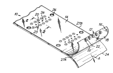
FIG. 1 13 a per~peotivQ v~w of ~ aarrler
film fabric~ted ~n ac~ordance wlth the p~e~ent invan~
tlon
FIG. 2 ~3 an enlarged, cros~-sectional view~
~aken sub~tantlally along th~ line 2-2 of FIG. 1;
FIG. 3 i~ a schematic view illu~trating th~
USQ of the carrl~r ~ilm in con~unction with th~ con-
~ection o~ pins to a prin~d circUit board;
FIG. 4 i~ an enlarged, cros~-s~ctional ~l~w,
ta~en substantially along the line 4-4 of ~IG. 3,
showing a portion of tha carrier f1lm and a solder
preform ln po6ition adjacent th~ prlnted circutt board
and pin, immedIately prior to the application of heat;
FIG. 5 i~ the 8ame view a~ FIG. 4, ~msdi-
ately a~ter the applica~ion o~ heat;
FI~ a schematic V~RW illu~trating ~h~method of aa~mbly o~ the c~rrier filmt
FI~;. 7 ls an exploded, perspective view of a
sealing covHr ~or a hermetlcally s~al~d contain~r
which may b~ a~sembled u~ing the carrier fllm o~ the
pr~sent invention;
F~a. 8 i~ ~ chematic vlew illu~trating the
a~embly proces~ ~or th~ ~over depicted in FI~. 7;
FIG. ~ is an ~nlarged plan view, taken sub-
Rtantially along the l1ne 9-g of ~IG. 8; and
FIB. 10 i~ a further 8nlarged, cross-sa~-
t~onal view, ta~en cubstantially along th~ line 10-10
of FIG. 3.
-- 1 30951 0
-7-
Referrlng now ~o the drawing~, and in par-
ticular to FIGS. 1 and 2, a carrier film made in ac-
cordan~e Wlth the pre~ent inven~ion i~ generally de-
ai~natad at 10. Carrier ~ilm 10 comprise3 a he~t-
rc~is~an~ substrate 12 havinq two substantially ~lat
opposed surraces 14,1~. Su~face 16 of substrate 12 i~
coated wit~ ~ wa~er-soluble pressure-sensitive adhes-
iV~ 13, ~hich removably re~ains a plurallty of bodie~
~f ~eat fu~ible material on surface 16 of sub6trate
12. As shown i~ tratiYely in FIGS. 1 and 2, the
bodle~ o~ heat fusible material may comprise preformed
donut-~aped solder w~sher~ or rings, ~u~h a8 t~ose
typically used to mak3 electrical cDnnection~ between
conne~tor pins and printed CircUit boa~d~, a represen-
tatlve ring being designated at 20. Generally, each
solder ring 20 has a cantral hole 22 which is sized to
~it and ~lip over the item to be soldered, typically a
cylindrical connector p~n. Substrate 12 ~3 provided
with co~ræ~ponding generally ~ircular perforation~, a
represent~tive p~oration being de~ignated at 23 ln
FIGS. 1 and 2. The diame~er~ of perforations 23 are
cho~en ~o aS to ~e su~stantially t~e same as that Or
central hole~ 22, a~ shown mo~t cl~arly in FIG. 2.
Solder rings 20 may optional~y be coated with a s~it-
abla ~lux mat~r~ a~ (no~ shown), a~ is conventional in
the a~t.
Adh~sive la retains solder rings ~o in any
deslred array, t~e c~n~igur2~on or pattern of which
c~n be pred~termined to ma~ch the arrangement of the
connector pin~ or o~her items to be ~oldered. F~
illustra~ss a typi~al albeit exemplary patt~rn, in
which ~en solder rtngs 20 are arrayed in two parallel,
~p~oed-apart row~ o~ fi~e rings each. ~hese solder
rlngs 20 are intended to be used to ~onnect ten con-
-8- 13095'0
nactor pln~ to a circuit board in a m~tching pattern,
wl~h eac~ ~old~r ring 20 surrounding one of ~aid con-
ne~Qr pins, as w~ll be de~cribed more ~ully hereina~-
ter in connec~ion with FIG. 3.
Spaced per~orat~ons 23 o~ substratQ 12 ar~
al~o arrang~d to match th~ ~pacing o~ the i~ms to be
301dsred, And perforation~ 23 are posltioned 30 that
they are di~po~ed coaxially with cen~ral holes ~2 of
solder rlnga ~0, a~ ~hown b~st ln FI~. 2. The de~red
pattern o~ 301der ring 20 may ~9 repsAt~d a~ regular
intervals along carrier ~ilm lO, as shown in FIG. 1,
~o th~ the ~olderlng opara~ion can b~ ~onveniently
repsat~d, ~or sxample, at variou~ locations on ~he
same printed ~lrcuit board. It i~ to be understood,
ho~ever, that the bodles o~ heat fu~lble ma~erial may
~e preformed ~nto other sh~pes ~e.g., ~quare or r~c-
~angular frame~), and that they may be arranged ln
oonfiguration~ or pa~torn~ othsr than that shown il-
l~stra~ively in FIG. 1. Regardle~ o~ ths patt~rn or
conf~gura~ion cho~en, however, 1t ls in~ended that the
carri~r ~ilm 10 be plaoed over the item~ to b~ sold-
ered, wl~h ~aah body o~ h~t fu~ble ~aterlal ~ur-
~ound$ng or dispo~ed ad~acent to the a~ociated item
to be ~older~d, aq ds~cribed in fur~h~r d~tail b~low
in connection with ~IG. 3.
In the preferred e~bodiment, carrier film lO
al~o comprl~es a ralease lln~r ~4 which ls coexten6ive
~ith ~ilm lO and which 1~ r~ova~ly retained adjacent
~urface 1~ o~ ~ub~trate 12 by adhe~ive 18. Relea~e
liner 24 se~ve~ to protect the bodies of heat fus~le
mAt4rial whils ~t the sam~ tims facilitating the hand-
ling of carrisr ~ilm lo prior to USQ. IS ~8 preferred
that c:arr~er ~il~ 10, lnc:lud~ng release liner 24, b~
conf i~ured ao a strip or t;~p~3 ha~rin~ a long~tudinal
dimension which su~stantially exc~d3 its tran~verse
dlm~n~io~, wlth a p~r of ~ubst~ntially parallel ~p-
-9- ~ 130~510
p~ed edge~ along ~he longltud1nal d~men~ion. This
conflguration, in which the ~trip or ~ape ~ mo~t
pre~erably betw~en one and two ln~h~ wide, advantag~-
ously ena~le~ carr~er fll~ lO to b~ wound onto a spool
~0 ~acll~tate it~ ~ae ~ hown in FI~. 3), with re-
laa~ ltner ~4 alBo the~e~ore prevent~ng und8~ired
contact betw~en ths adheslva coat 18 on the sur~ace 16
of each wound layer with the non-Adhe3~ eoat~d sur-
facQ 14 o~ th~ suac~ ive wound lay~r of ca~rier f~lm
10. Relea~e liner 24 i8 pre~erably fabriqa~e~ of
papsr, al~hough any material which can ~asily be
pesl~d away from aub3trat4 12 (a~ shown by arrow A in
FIG. l) can be used, such mater~als be~ng well-known
in the art.
In order to ~unction a8 int~nded, sub~trate
12 of c~rrier f1lm lO ~u~t be capable o~ tran~portlng
heat to the ~odies o~ he~t ~U~iblQ material, but at
th~ ~ame tlm~ mu8~ it~lf b~ cap~ of w~t~ tanding
temp2ra~ure3 a~ or ~ htly above th~ meltlng te~pera-
ture o~ the heat ~usible ~aterial for at l~ast the
duration o~ the solderlng proce~. Th~refor~ e
pr~c~se eh~rac~ristics ~ho~en for ~ub~trate 12 will
depend upo~ the n~ture of the heat fusiblQ material
baing us~d.
In general, it ha~ been ~ound tha~ ~ubstrate
la ~u~t be heat-re~i3tant to a te~peratu~e which 1~ at
least 20~C ~bove th~ ~elt~ng point o~ the hsat ~usi~le
mat~rial. I~ wlll ~ evident to thoso s~illed in th~
art that ~or a ~VQn compo~itlon o~ ~ubf3trat~3 12, the
higher the melting t~mpsraturo o~ ths heat fusible
material beinq u~ed, the t~cker substratQ 12 mu~t b~
in order to with~tand the h~ghe~ soldering temper~t-
ure~ r~quire~. Conv~rsely, if th~ heat ~u~bl~ ~ate~-
ial balng u ~d has a lower ~elt~ng ts~perature, sub-
~trate 1~ may ba c~osen to ~e thinnqr. Tabla I set~
~orth se~eral 801d~r alloy~ which are commonly-used ln
-lo- 1 3u~5 1 0
the semiconductor electronics industry, together with
their respective melting tPmperatures or the ranges
thereof, and the range of the thickness which has been
found to be suitable for substrate 12.
TABLE I
MELTING SUBSTRATE
SOLDE~ ALLOY TEMPERATURE THICKNESS
52% Bi/32% Pb/16% Sn g6Oc .002-.003"
(Semalloy*1280)
60% Pb/40~ Sn 183-235~C .003-.006"
58% Bi/42% Sn 125-127C .004-.006"
80% ~u/20~ Sn 280C .006-.010l'
In Table I, a range of thickn~sses for substrate 12 is
given for each different solder material listed. In
each case, if the soldering operation requires full
soldering (i.e., complete melting of the heat fusible
material), then the thickness of substrate 12 should
be chosen at or near the higher end of the range
given. Conversely, if the soldering operation re-
quires only tack soldering (i.e., only localized melt-
ing of the heat fusible material), then the thickness
of substrate 12 may be chosen at or near the lower end
of the range given.
In one preferred embodiment of the inven-
tion, the heat fusible material out of which solder
rings 20 are fabricated is Semalloy* 1280, and sub-
strate 12 of carrier film 10 comprises a transparentfilm which is approximately 0.002 inches thick. A
suitable carrier film having a substrate of this de-
sired thickness, and which is coated on one surface
thereof with a water-soluble pressure-sensitive adhes-
ive, is available with a suitable release liner in theform of a tape or ribbon from ~dhesives Research, Inc.
* Trade Mark
:`~
1 3Uq51 0
of Glen Rock, Pennsylvania under the trade name Solu-
mask*7242. It has been found that this product has
acceptable characteristics of temperature resistance
and heat transport of the substrate, as well as water
S solubility of the adhesive, for use with solder rings
fabricated from Alloy 1280 and intended to be used to
connect a plurality of connector pins to a printed
circuit board. Moreover, this product has the addi-
tional characteristic that the substrate (as well as
the adhesive which is coated onto it) is water-sol-
uble, and it is therefore within the scope of the
present invention to provide a carrier film 10 in
which both the substrate 12 and the adhesive 18 are
water-soluble, a term which as used herein means that
the substrate and adhesive will dissolve in aqueous
solutions at room temperature or higher.
In another preferred embodiment of the in-
vention, substrate 12 of carrier film 10 comprises a
Mylar*material which is approximately .006 inches
thick, and which is available commercially from ~ent
Adhesives Product Company of Kent, Ohio, or from the
Electronics Materials Division of E. I. DuPont de
Nemours & Company, Inc. of Wilmington, Delaware. In
this embodiment, the carrier film is assembled by
coating the ~ylar*substrate with a water-soluble pres-
sure-sensitive adhesive which is available from the
aforementioned Adhesives Research, Inc. Because of
its increased thickness and chemical structure, the
use of a Myla~ material for substrate 12 provides a
more heat-resistant carrier film which is also non-
hygroscopic and less stretchable, and for these reas-
ons, this e~bodiment is preferred when using high-
melting heat fusible materials such as gold~tin al-
loys.
Due to its greater thickness and/or
strength, the use of Mylar* as the substrate for car-
* Trade Marks
,
-12- 13~513
rler ~llm 10 al~o allowe lnd~xing And~or ~pr~ket
holes ~o be punched along ~he edge~ or the ~ when
it i~ con~lgurQd a~ a tap~. Thus, oub~trate 12 of
carrier ~llm 10 i8 optionally provided wlth a series
of lndextng and/or ~proc~et hole~ 26 di3posed ad~acent
opposeq edge~ 27A, 27~ o~ ~ubstrate 12 and runn~n~
alonq the longitudlnal dlmen~ion o~ carrier ~11~ lo
(as shown illustratlvely ~ n FIG . l) . Indsxing holes
26 are adapted to ba usQd in con~unction wlth a con-
vent~o~al pl~-~e~d mechanism (not shown) ~o facllitate
continuoUs automatic advance~ent o~ carrier ~ilm 10
when desired.
Substrate 12 o~ carri~r ~ilm 10 may al50 be
provided wi~h a plurality o~ locating hole~, a rep-
resentativ~ one o~ whioh is de~ignated at 28 in FIGS.
1 and 2, the p~rpose o~ which 1~ to acco~modat~ a
printed clrçult board and connector pln conflguratlon
in whlch not all o~ ~h~ conn~ctor p$n~ rQquir~ ~old~r
connection~. Th~ num):~er, Qpacing, 8~ Z~ and location
of locating holas 28 ~ay be chosen ~o as to ~tch the
pattQrn of connec~or pins for which ~old~r connection~
are not ~equ~red~ Lccatlng holes 28 enable carrler
~lm 10 to fit over such ~onnector p~ns wi~hout tear-
ing. In the illustrative ~mbodi~snt ~hown in ~IG. 1,
a xow Or ~ive locating hole~ 28 i~ al~po8~d on carrier
~ 10 parall~l to and sub8tantially midway between
eacb p~lr of rows o~ ~older ring~ 20, but sligh~ly
of ~e~ tran8versely wi~h respect to the ~older rings
20.
RR~err~ng now to FICS. 3-5 ln addition to
th~ a~or6mentioned FIGS. 1 a~d 2, carrier ~1~ 10 can
b~ illustr~tlvely utili2ed in tha manner sho~n in F~.
3 to ~acilitat~ the attachmen~ o~ a plurality o~ con-
nQctor pins to a prlnted clrcuit board. A8 ~hown in
FlG. 3, carrier fil~ lo is provided ln the rorm of a
t~p~ or ribbon wound around a hub 30 to ~or~ a roll
-13 1 30q 51 0
31. ~ub 3C 1~ ~ounted ~or r~tation upon A spindle
31A, and may be unwound in tha direction ~hown by
ar~o~ ~ and ~hereaft~r advsn~d laterally in th~ dir-
~ctlon shown by arrow C. Immadlat~ly prior to u~e,
~elea~e lin~r 24 o~ carrler ~ilm 10 iA peeled bac~,
and may be at~ch~d ~o and wound ln th~ directlon
6hown by arrow D around a hub 32 mount~d for rotation
upon a sp~ndl~ 33A to for~ ~ r~lea~ liner roll 33
w~ch ~ay ~e di~ard~d or pr~s~r~ed ~or subsequent re-
u~e.
A8 shown in phantom line~ ln FIG. 3, ~ub-
strate 12, wlth ~older rlngs 20 dispo~ed and retalned
on the lower sur~aae th~reof ~y means o~ adhe6i~ 18,
iB ini~lally dl~posed above and ad~acsnt an array of
connector pin~ 34,35 which have b*en prepo~ltioned ~n
a prlnt~d clrcuit boa~d 36 which res~s on a 3uppor~ing
me~ber 37. It 6hould be unders~ood tha~ in th~ illu~
tr~ivQ configuration depicted ln FIG. 3, each of
connector p~ns 34 ~ intendad to rec~ive a sold~r ring
20, whila each of conn~ctor pin~ 35 i~ lntended not to
recsive a solde~ ring 20. Wh~le conn~ctor pin~ 35 are
~how~ a~ being 3ho~er than conn~ctor ptn~ 34, it
should be under~tood that thi3 is ~or purpo~s o~
illustration only, and that connector p~ns 35 may 4e
th~ e l~ngth as, or ~onger than, ~onnector pins 34.
It ~hould also be understood that FIG. 3 i8 an edge
view, and thzlt b~hlnd eaah o~ connector pins 34,35
dep~cted ln FI~. 3 are four add1t~onal identical con-
ne~tor pins ext~ndlng in a parallel row below th~
plan~ o~ th8 drawing, non~ of wh~ch are vi~ible in
FI~. 3.
A~ shown more clearly in FIG. 4, each of
conn~ctor pln~ 34 ~s 1003ely supported in print~d
clr~u~t board 36 prior to th~ 601d~ring operat~on by
mean~ o~ a receivlng hol~ 38, a plural~ty o~ which are
provldQd in a patt~rn corre~ponding to the patt~rn of
- 1307513
-14-
conne~or pin~ 34 whic~ r~qulr~ otrlcal connection
to print~d cir~ui~ ~oarR 3G. It 1~ to ~ und~rstood
that conneator plns ~5 may al~o be supported i~ prin-
~ed oircuit boara 36 by ~an~ o~ 31mllar re~ ing
holes (not ~hown).
Af~r carri~r ~il~ 10 18 posit~on~d above
connQctor pin~ 34,35, carrier ~11~ lo ~ th~n moved
down~ardly toward conn~ctor pln~ 34,35 (in the dlrec-
tion shown by Arrow E in FIG. 3), such that locat~ng
holes 28 ~lt around connactor pins 35 and ~old3r rings
20 simultaneously flt over and around oonnector pin~
34, w$th connector pin8 34 pas~ing through the aentral
hole~ 2~ of ~older rlng~ 20 as w~ll a~ throuqh perfor-
atlons 23 i~ 4ubstrats 12, untll ~older rln~s 20 abut
the ~urfaca o~ prlnted circul~ board 35 and are ad~ac-
ent receiving holes 38, as shown ln solid lines in
FI~. 3 and a6 shown in further detall ln FI~. 4. At
thls point, tho edges of ~ub~trate 12 surrounding
conn~ctor pin~ 34 may be pre~s~d against printed cir-
cuit board 36 so tha~ adhesiv~ 18 conta~s the surfaceof prin~ed ~ircuit board 36 and thereby retains car-
~ier fil~ 10 and th~ solder rinq~ 20 d~po~od ther~on
in the desir~d lo~ation and con~iguratlon until the
~oldering operation takes pla~a.
A~ ~hown in FIG. 4, h~t may then b~ applied
by any suitable mQan3, all o~ wh~ch are conventional
an~ ~ro well ~nown in the art. FI~. 4 ill~Srate~
~chema~l~ally th~ use o~ a haating tool 39, which may
ta~e the ~or~ o~ an infrared hot shoe, a hot alr gun
or lamp, or an RF ~r~quency lmpul~e hea~r. It i8 to
b~ und~r~tood, how~v~r, that th~ soldering opera~lon
can be ~ccompli~hed ~n an alternative manner, such as
by h~atin~ ths entirQ prlnt~d circuit board ~n an oven
or belt ~urn~ae. Although the present inv~ntlon con-
templa~Qs the use of any one of th~ foregoing type~ ofh~at ~ources,. lt should bs under~tood tha~ ~f a h~at
130~510
-15-
~o~rc~ i~ cho~en wh~ch reguire~ direa~ phy~ical con-
tact b~tween ths heating ~lement and ~ub~trate 12 of
carrior fll~ 10 (e.g., if an infr~red hot ~hoe i8 used
as shown s¢he~a~lcally in FIG~ 4), t~n the ~hicknes~
of s~bs~rate 12 chould ~e choaen ~o a~ to be thick~r
than would oth~rwis~ be r~quired i~ a non-contaot heat
soUrce t~uch as an ov~n) w~re to be u~d under the
~ condltion~ ., uslng ~he same heat fu~lble
matRrial ) .
As shown in FIG. 5, the Appllcat~on of h~at
~t the approp~lat~ ~mperflture ~which is ~t or abou~
the molting tempQrature of the heat ~u~ible material,
and ~hich in any ev~nt ~8 well known to those skilled
in the art) cau~e~ each ~older ring 20 to melt 80 that
a portion 40 o~ the heat ~u~lble matsrial ~lows be-
tween each connQctor pin 34 and the corre~pond~nq
rQc~ving hol~ 38 in print~d circuit board ~6, with
the balance 42 o~ ~he heat fu~ible m~terlal remain~ng
on the ~urfac~ o~ printed circult board 36 and sur-
roundlng connector pin 34. An electrlcal and~or ~ech-
anical ~onnectlon batwe~n thR connector pin~ 34 and
th~ prlnted c~rcuit tnot ~hown) et~hed on print~d
circUit ~oard 36 about each recelving hole 38 i~
thereby created.
Th~ appropriats dur~tion for th~ applicatlon
o~ heat must b~ chosen such that lt endurQ~ until ~U8
be~oro th~ carrier fllm deforms and begins to ~hrin~
ThiR dtlration will vary dependlng upon several f ~c-
tors, such a~ the nature o~ the heating ~ource which
is to be us~d, and ~n some ca~es the thic~nes of th~
carr~er ~ subs~rato being used. For example, it
has be~n d~erm~ned that if the heat ~ource i3 chO8en
to be an in~rared hot ~hoe, as illustrated schematlc-
ally in ~IG. 4, and ~ th~ temp~ra ur~ o~ thQ hot shoe
i9 ~et at about 5'C above the mel~ing tempexa~ur~ of
th~ heat ~uslble ~ate~lal ~as i5 gener~lly pr~erred),
l3a~sl0
-16-
then the optimal duration for the application of heat
is approximately six seconds if the preferred embodi-
ment of the present invention is used in which the
carrier film is fabricated of Solumask*7242, as de-
scribed hereinabove, and is approximately eleven sec-
onds if the preferred embodiment of the invention is
used in which the carrier film substrate is not water-
soluble and is fabricated of Mylar*, as also described
hereinabove. In either case, the hot shoe is prefer-
ably applied with light pressure, e.g., at approxi-
mately 20 pounds per square inch of carrier film,
provided that no more than half of each square inch of
carrier film is covered by heat fusible material.
On the other hand, if a typical non-contact
heat source such as a convection oven is to be used,
and if the desired oven temperature is pre-set at or
about the melting temperature of the heat fusible
material (as is generally preferred), then it has been
determined that regardless of the thickness of the
carrier fil~ substrate being used, the optimal dura-
tion for the application of heat substantially corres-
ponds to the heating cycle of the oven, i.e., the time
it normally takes for the oven temperature to rise
from room temperature to the desired pre-set temper-
ature and to fall back again to room temperature,assuming that the oven is shut off immediately upon
reaching the deæired pre-set temperature.
Due to the heat-resistant characteristics of
carrier film 10, residual amounts of substrate 12 and
adhesive 18 remain in the vicinity of each connector
pin 34 after the application of heat, as shown in
phantom lines in FIG. 5 and designated at 44. How-
ever, a conventional hot aqueous bath can thereafter
be used to remove completely any residual water-
soluble adhesive, and will also remove any residualsubstrate if that substrate is also water-soluble, in
-17- 130)~,19
accordance with one of the preferred embodiments of
the present invention as described hereinabove. If,
on the other hand, the substrate is non-water-soluble,
in accordanqe with another preferred embodiment o~ the
invention as described above, a hot aqueous bath can
still be used to dissolve and thereby remove any re-
sidual adhesive, after which the residual substrate
may then be removed by peeling and discarded.
With the embodiment of the present invention
utilizing Solumask* 7242, in which the carrier film
substrate and the adhesive are both water-soluble, the
hot aqueous bath is preferably carried out using a
detergent solution in which the temperature of the
water is maintained at between 90F and 180F, and in
which the detergent is biodegradable and incorporates
both a wetting agent and no more than approximately
7.3% phosphorous by weiqht. A suitable detergent is
available commercially from Alconox Inc. of New York,
New York, under the trade name Alconox* and a suitable
detergent solution comprises between 0.7~ and 1.1
ounces of Alconox*detergent per qallon of water, the
water preferably being of electronic grade (i.e.,
grade E-lll or better).
This detergent solution is preferably ap-
plied to the assembled electronic components carryingthe residual substrate and adhesive, either by manual
agitation or most preferably using a mechanical washer
capable of spray circulation, for 2-5 minutes. The
detergent solution is thereafter removed, and a clean
warm or hot water rinse is then applied, also for 2 5
minutss, followed by a second rinse for 1-2 minutes,
both rinses also being applied either by manual agita-
tion or preferably by mechanical spray circulation.
Thereafter~ the assemblage may be heated for drying
using hot air maintained at a temperature which is no
higher than the highest temperature which can be tol-
* Trade Marks
1309510
-18-
erated by the assembled electronic components.
A similar aqueous bathing operation, using
the same preferred detergent solution, may be utilized
to remove any water-soluble adhesive remaining after
the soldering operation is performed with the pre-
ferred embodiment of the present invention in which
the carrier film substrate is not water-soluble and is
fabricated of Mylar* In this case, however, the as-
sembled electronic components may be fragile, and
rather than applying the detergent solution ~y manual
agitation or by mechanical spray circulation, the
electronic components are preferably subjected to
ultrasonic agitation in an aqueous bath in order to
remove both the residual adhesive and any residual
Mylar* substrate, following which the components are
blow-dried using hot air at approximately 110F.
For some applications, the use of a conven-
tional hot aqueous bath following the soldering opera-
tion may be undesirable and/or deleterious to the
electronic components involved. It has been deter-
mined, however, that the water-soluble adhesive used
in all of the carrier films of the present invention,
as well as the carrier film substrate of the embodi-
ment of the invention utilizing Solumask* 7242, can
also be dissolved in and completely removed using
certain non-aqueous solubilizing agents. In partic-
ular, it h~s been found that propylene glycol mono-
ethyl ether, available from Union Carbide Corporation
of Moorestown, New Jersey, under the trade name Propa-
sol Sclvent M*, as well as vinyl 2-ethylhexyl ether
(2), available from the Chemical Division of BASF Inc.
of Parsippany, New Jersey, are acceptable and effec-
tive alternative solubilizing agents for use with the
present invention. Either one of these solvents may
be applied at room temperature by submerging the as-
sembled electronic components in a container of either
* Trade Marks
-19- ~ J q s ~ o
liquid for approximately three minutes, followed by
submerging them in 1,1,1, trichloroethane for approxi-
mately one minute, followed by submerging them for
thirty seconds in a ~reon and methylene chloride mix-
ture, such as that commercially available from theGenesolv/Baron-Blakeslee Division of Allied-Signal
Inc. of Parsippany, New Jersey, under the trade name
Genesolv DM. The components are then blow-dried using
hot air at approximately llO-F.
It will be appreciated by those skilled in
the art that the water-soluble adhesive, which is an
essential component of the carrier film of the present
invention, not only retains the bodies of heat fusible
material in a fixed array, pattern, or configuration
on the carrier film substrate prior to the soldering
operation, but also leaves no residue and requires no
special removal procedure other than an aqueous bath
at conventional hydrocleaning temperatures. It will
also be appreciated by those skilled in the art that
neither the adhesive nor the carrier film substrate
will degrade at conventional soldering temperatures
and both are capable of transferring heat quickly to
the bodies of heat fusible material, and that these
are also essential components of the carrier film of
the present invention.
In the embodiment of the present invention
utilizing Solumas~ 7242, in which the carrier film
substrate and the adhesive are both water-soluble,
additional advantages are obtained. Specifically, the
water solubility of the substrate enables the user to
deform and mold the carrier film into non-linear
shapes (including, e.g., acute and right angles) prior
to the soldering operation, in order to match or con-
form the carrier film to the shape of the components
to be soldered. This deformation can be accomplished
manually, merely by bending the carrier film, but is
-20- - 1 3 ~"J5l 0
preferably facilitated by the application of a small
amount of moisture to the substrate in order to make
the carrier film more pliable. The embodiment of the
present invention, in which the carrier film substrate
is not water-soluble and is fabricated of Mylar* can
be similarly deformed by the user, provided it is pre-
perforated in an appropriate manner to create the
necessary flexibility.
A further advantage which is obtained with
lo the embodiment of the present invention utilizing
Solumask*7242 relates to the use of solder flux. If
solder rings 20 are optionally pre-coated with a flux
material, then residue 44 (shown in FIG. 5~ may also
include a quantity of unused flux. As is well known
in the art, any residual flux remaining after the
soldering operation must be removed, and the removal
operation can conventionally be facilitated either by
using only water-soluble fluxes, or by mixing water-
soluble fluxes with conventional non-water-soluble
fluxes, thereby permitting the fluxes to be washed
away in an aqueous bath after the soldering operation
is complete.
It has been found that the embodiment of the
present invention utilizing the Solumask*7242 product
of Adhesives Research, Inc. further facilitates this
operation by permitting incorporation of a water-sol-
uble flux directly into the water-soluble substrate,
and therefore provides an advantageous facility for
introducing a water-soluble flux into the soldering
operation. Using a vehicle such as methylethylketone
( or any non-miscible al¢ohol such a~ anhydrous isopro-
pyl alcohol), one or more water-soluble fluxes can be
transferred to the carrier film 10 by any suitable
coatinq process.
3s An example of a water-soluble flux which is
available in liquid form and which can be incorporated
.~ ~
-21- -- l 3~510
into the carrier film 10 of the present invention in
the manner described is water-soluble Organic Flux
2331, available from the Xester Solder Division of
Litton Industries of Chicago, Illinois. This flux
material can be applied either by dissolving it into
methylethylketone to form a 50/50 solution by volume,
or by dissolving it in anhydrous isopropyl alcohol to
form a solution which is 75% alcohol by volume (the
latter solution being the one preferred). In either
case the solution is lightly wiped onto the adhesive-
coated surface of the carrier film substrate in the
vicinity of the solder preforms, and/or onto the sol-
der preforms themselves, using a con~entional syn-
thetic cellulose sponge, and is then allowed to dry in
air.
It has also been found that the heat resis-
tant characteristics of a carrier film fabricated
according to the embodiment of the present invention
which utilizes Solumask*724~ can be effectively in-
creased by spreading cornstarchj dissolved either inanhydrous isopropyl alcohol or in water, onto the
water-soluble substrate prior to use, thereby increas-
ing its effective density. This can be accomplished
either by dissolving 6 ounces of a commercial grade
baking cornstarch in 32 ounces of anhydrous isopropyl
alcohol, or by dissolving 4-~ ounces of such corn-
starch in 30 milliliters of water, to form a solution
which in either case is then wiped onto the substrate
using a conventional synthetic cellulose sponge and
then dried using an infrared heat lamp at approxi-
mately 80~F for approximately one and one-half minutes
until dry.
Although the aqueous cornstarch solution has
been found to be more effective than the alcoholic
solution, the agueous solution is at the same time
more dif f icult to apply because the water-soluble
-- 130~510
-22-
substrate will dissolve if excessive amounts of the
aqueous cornstarch solution are applied. This effect
can be avoided by observing the color of the substrate
during the wiping operation, and by terminating the
application of the aqueous cornstarch solution after
the substrate becomes slightly milky in colcr. While
the use of the alcoholic cornstarch solution will
eliminate this undesirable solubilization of the sub-
strate, the alcoholic solution is less effective in
increasing the effective density of the substrate.
In either case, the use of cornstarch in
this manner enables the carrier film to withstand
higher soldering temperatures without degrading, and
therefore enables the use of higher-melting heat fus-
ible materials than would otherwise be possible for agiven thickness of the carrier film substrate~ For
example, although the Solumask*7242 product is norm-
ally not usable with heat fusible materials having
melting temperatures higher than about 255~C, the
incorporation of cornstarch in the manner described
above permits this embodiment of the invention to be
used with higher-melting heat fusible materials, hav-
ing melting temperatures as high as 290C.
It has been found that the heat-resistant
characteristics of a carrier film fabricated in accor-
dance with the embodiment of the present invention
which utilizes Solumas~ 7242 can also be effectively
raised by dissolving nitrocellulose into the carrier
film substrate, using methylethylketone or anhydrous
isopropyl alcohol as a vehicle and thinner for the
nitrocellulose. This method is preferred over the use
of cornstarch as described above, and is most effec-
tive if pure nitrocellulose, available from Stan-Chem
Incorporated of East Berlin, Connecticut, is used.
The incorporation of ni~rocellulose can be accom-
plished either by combining one-half ounce of pure
-23- -- 130q510
nitrocellulo~e ~or ov~ to-an ouncd~ of m~thyl-
ethylk~one~, or by combinlng ono-half` ounce o~ pure
ni~roc:~llulo~ ~or every ten ounc~ o~ anhydrous ~ ~o-
pr~pyl al¢ohol ~ to form ~ ~olutlon wl~loh in ~ith~r
ca~o i~ wip~d onto the carrl~r f llm ~ rato u~lng a
conventional E~yr~thc~tlc cellulo~s sponge and ~ then
allowlad to dry 1 n air. It has been ~ound that when
methylethylketon~ i~ u~d ~ the veh~cle and thinner
~or the nitrocellulo~a, the ~ir drying operation con-
sum~ time than wh~n anhydrous isopropyl alcohol
i8 U8Qd, and there~ore th~ u~e of ~ethylethylX~tone
p~e~erred.
Although ni roc~llulo~ i8 not usually w~t-
er~solubl~, it has b~en found th~t whon incorporat~d
~5 into ~he carrisr $1lm of ths pr~Bent invention ln thQ
~anner dQgarlbed~ any ra~dual nitrocellulo6e remain-
ing a~te~ the ~old~ring operation 15 compl~ can ~e
d~ssolv~d an~ thereby ramov~d in A conventional hot
aqueou~ ba~h.
A carrl~r fllm accordlng to the prs~ent
invent~on can be ass~mbled in a mannor Whi¢h is dep~c-
tod ~ch~matlcally ln FIG. 6. In par~cula~, ~ supply
roll 46 o~ the c~rrl~3r film to be usQd (e.g., Solumas~
7242 ) i~ mount~ or rotation on a spindlQ 47 . A5
~oll 46 unwind~ ~n the d~rection ~hown by ar~ow F~ th~
rsl~lasa liner 24 i~ pe~led back ~rom substrate 12, and
~ tra~nsd ~bout pul~ey~ 48 for transport in thQ dl-
rectlon ~hown by arrt)w G and ev~n~u~l reunlon with
~ub~trate 1~. Tna latter, w~th adhe~lvo ~8 coated or,
o~le ~urfacs 16 thereof, 15 trained about pullay~ 4~,
and p~Q~ through a di~ 50. A ~ourc~ ~not ~hotrn) of
bodies o~ a~ fu~ibl~ ma~ar$zll, such a~ preformsd
~old~r rln~s 20, ls located ad~cent die So, which may
~e operatad slth~r manually or ~n an auto~atad ~ashion
to affix solder rlngs 20 ~o ths ~dhe~ivOE-co~ted r~ur-
~ace o~ tra~ 12 ~ n the deslred pa~tern or con~ig~
-24- . ~ 3 G!~ 51 0
~ratlon, while at tha ~am~ ti~ c~eAt~ng perforations
23 ~hown b~t ln FIG. 2) in ~lignme~t with the cen-
trAl hol~a 22 Or sold~r ring~ 20.
~t~r sub~trat~ 12 p~s~e~ throu~h tho dle,
a~ ~own in FIG. 6 rel~A~e lln~r ~.4 i~ th~rea~ter re-
~o~ned wit~ substrate 12, by r~ttachlng t~Q rel~ase
lln~r 24 to ths surface 16 of sub~trate 12 carrying
adhesiv~ 18, ollow~ng wh~ch the a~se~bled carr$er
film 10 1~ wound onto a tak~-up roll 52 wh~ch is moun-
ted ~or rQtation on ~pindl~ 53 in th~ di~ection ~hown
by arrow H. It in contemplats~ t~at the a~aem~ly pro-
ce~ur~ deploted schs~atically ln FIG. 5 can be auto~a-
ted, in which ca~e ~pln~le 53 WOUld b~ appropriately
connect~d to and driven by driva ~an~ ~not shown)
which would al~o act or cooperat~ in a known mannsr
with rec~procatinq ~ean~ (not shown) to close the
~ating hal~es SOA, 50B o~ di~ ~0 at appropriat~ inter-
vals.
Re~erring now to FIGS. 7-10, a ~thod of
fa~ricatln~ ~ condu~lve h~r~etlc ~0al~ng cover for a
conta~nQr hou~ing a ~emicon~uctor d~vic~, using th~
carrler 2ilm of th~ pres0nt lnvQntion, is illustrated
thore~n. A~ ~hown in FIG. ~, a conventional conduc-
t~ hermetic ~ealln~ cover, gen~rally des~gnated at
54, comprlse~ a ~lat me~allic lid 55 and a pre$o~med
ring or ~ram~ 58 ~hich is fabrlcated of a heat ~usible
materi~l and whtch i8 supe~impose~ upon and at~ached
~o th~ lid 56 in registry with the perlph~ry thereo~
As ~ot ~orth h~elnabove~ ~ch s~alln~ cover3 are
- 30 ~yplcally u~ed to s~al tha cavity o~ ~ semiconductor
packag~ which ~ay co~tal~ ~n ~atl~e $nt~gratQd-circuit
3ili¢0n chlp. For most applicatlons, the lid 56 ~
~abri~at~d of a nlck~l-cobalt-lron alloy, widely mar-
X~ted undsr the trade name KOVAR, w~ic~ i~ subse
qusntly gold-platsdr and in ~a~y appl1cation~, the
fram~ ~8 o~ hea~ ~u~ible material co~pr~s~s a gold-tin
- 130~510
-25-
eutectic solder, although other solder alloys such as
lead-tin are also sometimes used. The sealing cover
54 is typically provided as a unit, with the solder
frame 58 pre-attached to the periphery of the lid 56
by heating the frame to a fusing temperature at a
plurality of spaced points (e.g., at the four corners)
in a spot welding operation which typically requires
that the frames and lids be manually fed into the
attachment apparatus.
The carrier film of the present invention
can be advantageously utilized to automate the previ-
ously described assembly process, as shown schematic-
ally in FIG. 8. A plurality of solder frames 58 are
mounted sequentially on a dispensing tape 60 which is
fabricated in accordance with one of the preferred
embodiments of the present invention described above,
in which the carrier film substrate is not water-
soluble and is fabricated of Mylar*which is approxi-
mately .006 inches thick. The dispensing tape 60
carrying frames 58 is wound onto a supply roll 62 from
whieh a release liner 64 is peeled back as supply roll
62 is unwound in the direction shown by arrow J,
thereby exposing the adhesive-coated surface 68 of
tape substrate 66 on which frames 58 are disposed.
Similarly, a plurality of lids 56 are mounted sequen-
tially along a second dispensing tapa 70, also fabri-
cated in ac:cordance with the same embodiment of the
present invention. The dispensing tape 70 carrying
lids 56 is wound onto a supply roll 72, from which a
release liner 74 is peeled back as supply roll 72 is
unwound in the direction shown by arrow K, thereby
exposing the adhesive-coated surface 78 of tape sub-
strate 76 on which lids 56 are disposed.
By means of an appropriate roller and/or
pulley arrangement (includinq, for example, roller 79
in FIG. 8), the adhesive-coa~ed surface 68 of dispen-
- 1 30~51 0
-26-
sing tap~ fio i~ the~l brought into ~ac~ng r~lation wlth
tho adhesivo coat~d sur~c~ 78 o~ dlap~n~ing tap~ 70,
such tha~ each ~rama 58 mou~t~d on dl~pen~lng taps 60
i~ ~lspo3ed ad~scent ~o and i8 sup~rimpOsQd upon a
Corre~ponding lld ~6 mounted on dispensing tape 70,
wit~ each f~am~ 58 in regi~try with ~ha periphery o~
th~ correapond~ng lid 56, as shown b~t in FIG~. g and
10 .
~h~le malnt~ning th~s facing relatlon~hip,
1~ di3pQnsing tape~ 60 and 70 ~re pa~s~d through a tuck-
ing ~ean~, ~hown lllustratively in F~G. 8 aR comprie-
~ng flnger~ 80A, 80~. PrQ~ar~bly, flnger 80A r~ma~n~
stationary, whil~ flnger AOB r~clprocat4~ ~n the d~r-
ection shown by arrow ~ between an active po~it~on
(shown in FIG. 8) in whi¢h one end 80C $B in Cont~ct
wlth sUbstra~e 76 o~ disp~nsing ~ap~ 70, and an lnac-
tive po~itlon (not ~hown) in which it is out o~ ~on-
~act with ~ub~tra~ 76 o~ dispensing tape 70. The end
portion 80C of ~inger ~OB 18 generally arcuata in
sh~pe, and ~inger 80B i9 drlven repetitively $nto and
out of contact wit~ ~ub3trate 76 ~y re¢lprocat$ng ox
cam ~ean~ ~not shown), with the interval batween ~uc-
ceJ~ive r~c~procations o~ f~nger 80B be~ng cho~en such
that said contact occurs only in the areas betwean
su~ce~ e lld8 56 mount~d on di~pens~ng tapo 70.
A~ b~3t shown in FIG. 10, each ~ucces~ve
reclp~ocat~on o~ ~inger 80B urg~ ~ub~t~ate ?6 of
d~Bpensing tupe 70 towarda ~ub8trate 66 o~ dispen8$n~
tape 60l 8U~h that the adhe~ive-coa~ed ~ur~ace 78 of
d~pon~ng tape 70 contact~ the adhe~lv~-coat~d ~ur-
~ace 68 o~ dispen~ng tape 60, ~orming a tuck or r~-
c~s~ 81 in ~ 8t~at~ 76 of di~penslng tap~ 70, wh~ch
pro~r~bly ext~nds tran~vQrssly ~ro~ o~e edge of sub-
strat~ 76 to.the oth~r ed~e. The contact between th~
w~ter-601uble adh~slve coate~ on ~urface 68 o~ sub~
8trate 66 and the w~ter-801uble adh~lvo coatad on
-27- 1309510
surfac~ 78 o~ su~S~rate 7~ wh1ch ~orm3 recesses 81 i~
su~icient to flx ~he po~lon~ of each ~ucces~ive
l~d/fram~ p~ir euch that th~ regi~tration of each
~rame 56 with the periph~ry of the as~oclat~d lid S6
5 i8 malntained prlor to ~nd during the ~ub~eguent a~-
tachment ~t~p.
In this con~iguration, the di~pensing ~apes
60,70 are advanced ~oward~ an attachment means, whlch
~llu~trat$vsly comprises a ~pot wslding apparatu~
dep~cted ~chem~tic~lly at 82 in FIa~ 8. Such spot
welding appar~tu~ are well known in the art, and typ-
ically comprise a w~lding head 84 d~spo~e~ abo~e a
support~ng me~b~r 85, one ~uch apparatu~ being de-
scribed ln detail in U.S. Patent No. 3,946,1~0. It
will b~ understood by thQs~ ~k~lled in th~ art that
the conventlonal 5pot welding ope~ation can take pl~ce
despite the ~ac~ that ~ubstrate 66 of dispen~n~ t~pe
60 prevent~ dlrect contac~ between thQ welding elec-
trGdes (not shown) of the weldlng h~ad 84 and each
~uc¢essive frame 58, dus to ~h~ heat transpor~ and
heat resistant characteristic o~ the dlspen~ing tape
60 as de~cribed hereinabove.
T~e attachment operation result~ in an e~-
~ect~ve at~Achment b~twean each lld 56 and the ~or-
responding frame ~8, ~oxm~ng a~seFbled covers de~ig-
nat~d at 86 in FI~. 8. Thereafter, the dispensing
tap~ 70 is paF.6Qd throu~h str~pping means, repre8ented
w hematically ln FIG. 8 by roller 87, which effects
xemoval o~ ~ubstrate 76 ~ro~ the a ~embled covers 86,
a~ter which ~ubstrat~ 7~ may be discarded or recycle~
~or 3u~8~quant U5~. Substrat~ ~6, on which ~he ~s~e~-
bled covers 86 remain di~posed, i~ then re~oin~d with
a r~l~a~ linqr 88, and i~ wound in th~ ~irection of
arrow L on a take-up roll so. T~e a~sem~led coverq 86
3S may b~ pro~ided in thls form, or may alternativ~ly be
removed fro~ th~ tap~. and r~packagad, ~3r subsequen~
130"510
-28-
U8~ in ~ h~rme~lc se~lln~ vperatlon to cover a con-
tainer hou~ing a ~emiconductor devi~e.
I~ de~ired, the residual water-solubl~ adhe-
sive remalning on th~ ~ur~aco 89 o~ each as~em~led
cover 8~ that was previously ln contact wlth ths adhe-
siv~-coated ~ur~a~ 78 of ~ub~tr~t~ 76 ean be removed
by pa~ing ~ wa~r-impregnat~d hard ~pon~e ove~ each
~urface 89, either prior to ~h~ r~oining of relea~
liner 88, or ln a 3ub~equsnt sep~rate r~n~ng opera-
10 tion. }~owev~r, lt has b~r, discovered that the re~id-
ual adheslve can ~erv~ as A watting agent, which will
~acilitate th~ creatlon of a hermetic ~eal when the
a~embled ~overs 86 ~rs su~e~u~ntly u~ed to saal a
container housing a ~emicondu~or device. Therefors,
~t 1~ within the scope of this embod~mont of th~ in-
vention that th~ step of removlng any residual adhes-
iv~ be omitted.
As shown in ~IG. 9, e~thsr or both of di~-
pens~ng tapes 60,70 can b~ provided optionally with
~pr w ket holes ~2 located ad~acent the oppo ed paral-
lel Edges 94A,94~ o~ ths tape (8) and running along the
longitudlnal di~Qnsion th~reo~. ~he ~pro~ket hol4s
92 ars adaptad ~o cooperata with ~onventional pln ~e~d
means (not shown) to ~dvanc~ th~ di3pen6ing tape~ and
2~ ~er~y auto~at~ still ~urther tho fabricating ~e~hod
o~ the inventlon.
Whlle there has besn descri~ed what are, at
pre~nt, con~ldered to b~ th~ pre~erred embodimQnt~ of
the invBnt~ on, it will be obviou~ to those sklllQd in
th~ art th~t v~riou~ ohanges and modi~lcations ~ay be
mada therain, wlthout depar~ing ~rom the ln~ention,
and it ls, there~or~, almed in the appended claim~ to
cov~r all such change~ and mcd~fication~ ae fall with-
in the tru~ spirit and scope of the invention.