Note: Descriptions are shown in the official language in which they were submitted.
1 309665
Title of the Invention
AMPLITUDE COMPRESSING/EXPANDING CIRCUIT
BACKGROUND OF THE INVENTION
... . . .
Field of the Invention
The present invention relates to an amplitude
compressing/expanding circuit which is suitable for use
in signal processing circuits of electronic appliances
such as a compact disc (CD) player and a tape recorder.
BRIEF DESCRIPTION OF THE DRAWINGS
For a better understanding of these and other
objects of the present invention, reference is made to
the following detailed description of the invention to
be read in conjunction with the following drawings, in
which:
Fig. 1 is a characteristic curve diagram used for
explaining problems in the prior art amplitude
compressing/expanding circuit;
;' Figs. 2 and 3 are schematic block diagrams of the
` conventional amplitude compressing/expanding circuit;
Fig. 4 is a schematic block diagram of a basic
circuit arrangement of an amplitude '~~
1 3096`65
compressing/expanding circuit according to the
invention;
Figs. ~ through 12 illustrate characteristic curve
diagrams used for explaining various operations of the
amplitude compressing/expanding circuit shown in Fig. 4;
Fig. 13 is a characteristic curve diagram for
sho~ling a loudness curve;
Figs. 14 and 15 are characteristic curve diagrams
for explaining operations of amplitude
compressing/expanding circuits according to other
preferred embodiments;
Fig. 16 is a schematic block diagram of one example
of the control signal generator shown in Fig. 4;
Fig. 17 is a characteristic curve diagrams used for
explaining operations of the amplitude
compressing/expanding circuit shown in Fig. 16;
Figs. 18 and 20 are schematic block diagrams for
showing a portion of the equivalent circuit shown in
Fig. 16;
Figs. 19 and 21 are characteristic diayrams used
for describing the operation of the control signal
generator illustrated in Fig. 16;
Figs. 22 and ~3 represent data example used for
explaining the o~eration of the control signal generator
shown i~ Fig. 16;
~ ig. 24 is a schematic block diagram of a control
signal generator according to another preferred
embodiment;
-- 2
1 3~966S
Fig. 25 is a circuit diagram of a portion of the
amplitude compressing/expanding circuit shown in Fig. 4;
Fig. 26 is a schematic block diagram for
illustrating an equivalent circuit of the circuit shown
in Fig. 25;
Fig. 27 to 30 are characteristic curve diagrams
used for explaining the operations of the circuit shown
in Fig. 25;
Fig. 31 is a schematic block diayram of an
amplitude compressing/expanding circuit according to
another preferred embodiment of the invention;
Fig. 32 is a schematic block diagram of an
equivalent circuit of the circuit shown in Fi~. 31;
Fig. 33 is a schematic block diagram of an
amplitude compressing/expanding circuit according to a
modified preferred embodiment of the invention; and,
Fig. 34 is a characteristic curve diagram used for
explaining operations of the circuit shown in Fig. 33.
Prior Art
. .
:~ It has so far been practiced in digital audio
signal reproducing apparatus such as CD players and
digital audio tape recorders (DAT) that an audio signal
recordedr after being digitized, on a recording medium
is reproduced and thereafter demodulated into a
corresponding analog signal, whereby, a high-~uality
audio signal with little noise over a wide dynamic range
is obtained.
There is however a problem that an audio signal
obtained from such digital audio signal reproducing
apparatus has an unwanted wide dynamic range when, for
-- 3 --
- 1 ~l3~665
example, it is to be recorded by a conventional analog
type tape recorder.
That is, because of its unnecessary wide dynamic
range, when the reproduced analog signal is recorded by
an analog tape recorder, the signal waveform of this
audio signal is produced distortion at its higher signal
level portion or its SN (signal-to-noise) ratio suffers
deterioration, conversely, at its lower signal level
portion.
Further/ in the case where a CD player or the like
is played back where there is background noise, such as
within an automobile, there arises another problem that
the signal portion at the lower signal level is lost in
the background noise and becomes inaudible, or,
conversely, the signal portion at the higher signal
level produces excessively large volume of sound.
To solve such conventional problems, one of better
solutions is to reduce the dynamic range of the audio
signal obtained from the digital audio signal
reproducing apparatus.
That is, as shown in Fig. 1, in an input signal
constructed of an audio signal converted into an analog
signal, the input signal at the level lower than -30 dB
of the peak level may be output as an output signal
- 1 3D9~65
whose signal level varies proportionally to the
variation in the signal level of the input signal with a
constant o~ proportion of 1.
On the other hand, the input signal in the range
higher than -30 dB may be output such that it varies
proportionally to the variation in the signal level of
the input signal with a con~tant of proportion of, for
example, 1/2.
By so doing, an input-output characteristic having
the ratios of amplitude compression CR of values 1 and 2
in their respective ranges on both sides of the point at
-30 dB (hereinafter this point will be referred to as a
threshold point, or level) .is obtained, and thus, the
dynamic range of the audio signal as a.whole can
correspondingly be made narrower.
To obtain such an amplitude compressing and
expanding effect, there is a prior art method using an
amplitude compressing/expanding circuit of the structure
as shown in Fig. 2.
That is, an input signal SI is input to an
amplitude modulation circuit 3 through a delay circuit 2
and it is also input to a control signal generator
circuit 4.
- 5 -
1 30q665
The control signal generator circuit 4 detects the
signal level of the input signal and, based upon the
result of the detection, outputs a control signal SG/ of
which signal level changes in accordance with the signal
level of the input signal SI, to the amplitude
modulation circuit 3.
The amplitude modulation circuit 3 is constructed
of a multiplier circuit, VCA (voltage controlled
amplifier), or the like and, by having the input signal
SI amplitude-modulated by the control signal SGr
provides an output signal So whose signal level is
corresponding to the input signal SI and changed
according to the signal level of the control signal SG.
It should be noted that the delay circuit 2 is
provided so that no overshoot may occur in the output
signal So.
Now, representing the amplitude of the input signal
SI by "x" and the amplitude of the output signal So
by "y", the amplitude compression ratio CR can be
expressed as:
y = Xl/CR . . (1)
Therefore, in the control signal generator circuit
~, the amplitude y of the output signal So Of which
amplitude compression ratio CR applied to the amplitude
-- 6 --
1 30966S
x of the input signal SI below the threshold point is a
value of 1 is expressed as
Y = xl/cR
= x ~ X(l-cR~/cR
= x x
= x 1 ...(2)
Therefore, corresponding to the coefficient 1 of
the right side, by outputting the control signal SG SO
that the gain "g" in the amplitude modulation circuit 3
may become value 1 as expressed by
9 = 1, . ...(3)
the characteristic providing the amplitude compression
ratio CR of value 1 in the region below the threshold
point can be obtained.
In contrast thereto, in the case where the output
signal So, of which the amplitude compression ratio CR
applied to the amplitude x of the input signal SI in the
range above the threshold point is of a value of 2, is
to be obtained, the amplitude "y" of the output signal
SO and the gain "g" in the amplitude modulation circuit
3 are given by
Y = Xl/CR
= x . X(l-cR)/cR
= x . x-l/2 (
1 309665
9 = X(1-CR)/CR
= X-1/2 . . (5)
Therefore, by outputting the control signal SG SO
that the gain g in the amplitude modulation circuit 3
may become x-l/2! an input/output characteristic
providing the amplitude compression ratio CR of the
value of 2 in the range above the threshold point can be
obtained.
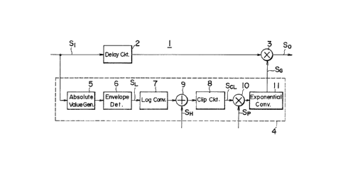
As a concrete example, the control signal generator
circuit 4 may be structured as shown in Fig. 3. That
is, the input signal SI is input through an absolute
value circuit 5 to an envelope detector circuit 6 and
thereby a detection signal SL proportional to the signal
level of-the input signal SI is obtained, and this
signal is then subjected to logarithmic conversion in a
logarithmic converter circuit 7 and output to an adder
circuit 9.
A clipping circuit 8 receives a summation signal of
the logarithmically-converted detection signal SL and a
threshold point signal SH provided through an adder
circuit 9, and clips the summation signal below a value
of O and output the thus obtained clipped signal SCL to
a multiplier circuit 10.
1 309665
Thus, setting the threshold point signal S~ to a
predetermined value enables a clipped signal SCL to be
obtained~ of which signal levels varies with respect to
both sides of the signal level of the input signal SI to
be determined by the threshold point signal SH.
The multiplier circuit 10 receives both the clipped
signal SCL and a compression ratio controlling signal Sp
and outputs a product signal thereof to the amplitude
modulation circuit 3 through an exponential converter
circuit 11.
Here, if the signal level of the input signal SI at
the threshold point (-30 dB in the present case) is
expressed by "Y" with respect to the signal level,
represented by H, of the output signal output from the
logarithmic converter circuit 7 when the input signal SI
is at its peak level. ~hen if the threshold point
signal SH is expressed as
SH = H - Y/20 loge 10 ..,(6)
accordingly, a clipped signal SCL whose signal level
varies with the signal level of the input signal SI only
when the signal level of the input signal SI is larger
than the signal level at the threshold point can be
obtained.
_ g _
1 309665
As a result, in the range below the threshold
point, the clipped signal SCL which has been clipped at
the value of 0 through the clipper circuit 8 is
obtained, and as a consequence, a control signal SG of
the value of 1 corresponding to the value of 0 is output
through the exponential converter circuit 11.
Consequently, the gain of the multiplier circuit 3
is limited to 1 and thereby, the output signal So of
which amplitude compression ratio CR is equal to the
value of 1 as shown in equation (2) is obtained, and
thus, the input/output characteristic producing the
amplitude compression ratio CR of the value of 1 is
obtained.
On the other hand, in the range above the threshold
point, it will be satisfied if the gain of the
multiplier circuit 3 is arranged to become x-l/2 as
indicated in equation (5).
That is, the below~mentioned control signal SG at
the signal level expressed as
SG = X(1-CR)/CR (7)
may be output with respect to the input signal SI.
More particularly, if the compression ratio
controlling signal Sp is supplied to the multipller
-- 10 --
1 309~65
.
circuit 10 so that the gain therein may become the value
expressed as
Ap = -(CR-l)/CR = -1/2 ...(B)
an output signal SO whose amplitude i6 compressed by the
compression ratio CR (CR = 2 in the present case) in the
range above the threshold point can be obtained.
Thus, an amplitude compre~sing/expanding circuit 1
of such an input/output characteristic that will change
the amplitude compression ratio CR from the value of 1
to the value of 2 when the signal level of the input
signal SI is increased across the signal level at -30
dB.
However, in the above-described conventional
circuit arrangement, there arises a problem that the
amplitude compression ratio CR abruptly changes between
the front range and the rear range of the threshold
point, and therefore, when the audio signal is
reproduced in the conventional amplitude
compressing/expanding circuit 1, the reproduced sound
produces extremely unnatural feeling to listeners.
To solve the above problem, one conventional method
has been proposed in such a manner that the amplitude
compression ratio CR is gently changed by gradually
changing the signal levels of the threshold point signal
,~;
1 309665
SH and the compression ratio controlling signal Sp in
accordance with a change in the signal level of the
input signal while employing, for example, a ROM (read
only memory) table.
~ lso, another conventional method has been proposed
that.the threshold point signai SB and the compression
ratio controlling signal Sp are controlled by the use of
a control circuit of a processing circuit arrangement,
instead of ROM table.
However, if such conventional methods are used,
there arises another problem that the construction of
the amplitude compressing/expanding circuit as a whole
becomes complex, and therefore, such methods are not yet
satisfactorily practicable in the recent technology.
Further, as the output signal SO of the above-
described amplitude compressing/expanding circuit, there
is only obtained such a multiplied output signal SO,
depending upon the control signal SG provided from the .
control signal generator circui1. 4, and therefore, there
is a problem that the operati.ng characteristic cannot be
made variable according to the frequencies of the input
signal.
The capability of making the operating
characteristic of amplitude compressing/expanding
- 12 -
`1 3~ Ji~)f~5
function variable with the frequencies of the input
signal will be widely applicable to various aspects of
the art specifically in handling audio signals. For
example, it will be applied to the compensation for the
audio signal of compressed amplitude to make up for the
feeling of lack of the dynamic range according to the
sense of hearing.
SUMMARY OF THE INVENTION
Accordingly, it is an object of the present
invention to provide an improved amplitude expander
and/or compressor circuit which is free from above-
mentioned drawbacks encountered in the prior art
ci~cuit.
It is another object of this invention to provide
an improved amplitude expander and/or compressor circuit
in which a desired input/output characteristics can be
obtained with a relatively simple circuit constructlon.
Still another object of the present invention is to
provide an improved amplitude expander and/or compressor
circuit in which an input/output characteristics can be
controlled in accordance with the frequencies of an
input signal.
- 13 -
- 1 3`D~6~5
,
Further ob~ect of this invention is to provide an
improved amplitude expander and/or compressor circuit in
which an input signal can be normalized in a high speed
with a simple circuit construction.
Still further object of this invention is to
provide an improved amplitude expander and/or compressor
circuit in which a smooth change in the amplitude
compression ratio near the threshold level of the input
signal can be obtained with a simple circuit
construction.
Yet further object oE this invention is to provide
an improved amplitude expander and/or compressor circuit
in which the amplitude compression ratio is changed
smoothly even with a plurality of amplitude compxession
changing points.
In order to solve the above-described conventional
problems, in an amplitude compressing/expanding circuit
according to the present invention, such that the
amplitude compression ratio for the output signal is
switchable by controlling to change the gain of the
amplitude modulating circuit based upon the signal level
of the input signal or output signal from the amplitude
modulating circuit, the amplitude compressing/expanding
circuit comprises an adder circuit for outputting a
- 14 -
~ l J ~ ~ ~ 5
difference signal between the input signal and output
signal, and a signal processing circuit for feeding out
an output signal whose si~nal level varies with the
difference signalr and is adapted to output a summation
signal of the output signals from the amplitude
modulating circuit and the si~nal processing circuit.
In ~ccordance with the amplitude
compressing/expanding circuit, when the difference
signal between he input signal and the output signal of
the amplitude modulating circuit is output through the
processing circuit so as to be added to the output
signal, a suitable input/output characteristic of the
processing circuit can be selected, and therefore the
summation signal varying, with a more preferable
input/output characteristic than that of the output
signal can be obtained.
.... .. .. . . . .
1 30~66~
DETAILED DESCRIPTION OF THE PREFERRED EMBODIMENT
One preferred embodiment according to the invention
will now be described with reference to the accompanyin~
drawings.
It should be noted that the same reference numerals
shown in Fig. 2 will be employed as those for denoting
the same or similar circuit elements shown in ~ig. 4.
In the circuit arrangement shown in Fig. 4, 20
denotes an amplitude compressing/expanding circuit as a
whole and the input signal SI and the output signal SO .
of the multiplier circuit 3 are received by an adder
circuit 21 and a difference signal SR therebetween is
supplied to a multiplier circuit 22.
The multiplier circuit 22 receives the control
signal SG as well as the difference signal SR and
supplies a product (multiplied) output signal of these
- 16 -
1 3 ~ 5
signals to an adder circuit 25 through a filter circuit
23 and an amplifier circuit 24.
As a result, in the adder circuit 25, when the
multiplier circuit 3 is operated under the condition of
an amplitude compressing operation with its gain set
below 1, an output signal Ss whose phase is put in
inverse relationship to with that of the output signal
SO through the amplifier cixcuit 24 is obtainedr and the
summation signal Sol of these output signals Ss and SO is
delivered therefrom as its output signal.
That is, the amplitude compressing/expanding
circuit 20 according to one preferred embodiment is
constructed oE a main pass circuit made up of the
multiplier circuit 3 ~or amplifying the input signal SI
by the gain corresponding to the control signal SG and
for outputting the amplified signal therefrom, and a
sub-pass circuit receiving the difference signal SR and
outputting the signal through the signal processing
circuit 26 constructed of the multiplier circuit 22,
filter circuit 23, and the amplifier circuit 24.
Therefore, in the case where the signal level of
the input signal SI is below the threshold point or
level, the gain "g" of the multiplier circuit 3 is set
to a value of 1, and hence, the signal level of the
1 309665
difference signal SR is kept at a value of ~, whereby
the output signal SO obtained by way of the main pass
circuit is output through the adder circuit 25.
On the other hand, i~ the signal level of the input
signal SI rises across the threshold point, the gain "g"
of the multiplier circuit 3 is switched to l/2, and
hence, the rise in the above-described signal level
follo~7s a rise in the ~ignal level of the difference
signal SR, whereby the signal level of the output signal
Ss provided by way of the sub-pass circuit is increased,
and the proportion of the output signal Ss to the output
signal SOI` is correspondingly increased.
Thus, by setting the input/output characteristic of
the signal processing circuit 26 forming the sub-pass
circuit to a suitable value r it is possible to obtain a
desired input/output characteristic which will provide
gradual variation in the signal level, describing a
gentle curve, of the out~ut signal SOl while the signal
level of the input signal SI is increased.
Now/ by letting both the gain of the multiplier
circuit 3 and that of the multiplier circuit 22 be "g"
respectively, while representing a transfer function of
the filter circuit 23 by F(~)and the gain of the
amplifier circuit 2~ by "A", an output signal SO, whose
- 18 -
1 3096~5
amplitude Zl is given by the following equation, is
obtained through the multiplier circuit 3
Zl = gx (9)
As a consequence, a difference signal SR whose
amplitude ZR is given by the following equation can be
obtained through he adder circuit 21
ZR Z1 -- X
= gx - x ...(10)
and an output signal Ss whose amplitude Z2 iS given by
the following equation can be obtained through the
signal processing circuit 26
Z2 = g A F (~) ZR
= g A F (~) ~ (gx - x) ...(11)
- Therefore, based on equations (9) and (11), an
output signal SOI whose amplitude Yl is given by the
following equation can be obtained
Yl = Zl - Z2
= gx - g-A-F(~) (gx - x)
= {(1 + F(~)-A) - F(~)-A-g}gx ...(12)
Then, letting the amplitude "x" and a transfer
function F(~) be x = 1, and F(~) = 1 respectively, if
the gains "g" of the multiplier circuits 3 and 22 are
changed between values O to 1, it becomes possible to
know output characteristics of the amplitude
-- 19 --
1 309665
compressing/expanding circuit ZQ at the times when the
signal level of the input signal SI is kept constant and
the amplitude compression control signal SG is varied.
That is, substituting these equations
F(~) = 1 ...(13)
x = 1 ...(14)
in equation (12), we obtain
Yl = {(1 + A) A g} g ...(15)
Then, the output characteristics, as shown in Fig.
5, are obtained, in which, while the gain "g" is varied
between the value of 0 an a value of 1, the gain of the
amplitude compressing/expanding circuit 20 as a whole is
maximum at the gain llgll of a value of 0.5 and the gain
of the circuit as a whole increases as the gain l'A" of
the amplifier circuit 24 is increased.
Further, when the gain A is kept at the value of 0,
if the gain g i5 changed from the value of 0 to the
value of 1, an output characteristic, in which the gain.
linearly increases therewith, of the main pass circuit
only is obtained, and when the gain A is of other values
than "0", the gains of the sub-pass circuit are
superposed on the gain of the main pass circuit, and
thereby, all the characteristics obtained have ascending
- 2~ -
1 309665
inclinations toward the right shown in the
characteristic curve diagram of Fig. 5.
Thus, by controlllng the gain of the sub-pass
circu.it, the gain of the amplitude compressing/expanding
circuit 20 as a whole can be controlled, and therefore,
the output signal SO1 varying with a desired
input/output characteristic corresponding to the
provision of the sub-pass circuit for the main pass
circuit can be obtained.
In the circuit arrangement of Fig. 4, if the
transfer function F(~) of the filter circuit 23 is set
to a value of 1, an operating characteristic provlding a
smooth change of the amplitude compression ratio C~ is
obtained, and further, by setting the gain A of the
amplifier circuit 24 to a specific value, it becomes
possible to perform both the amplitude compressing
operation and amplitude expanding operation at the same
time.
Here, the preferred embodiment will be examined as
to the case where the threshold point is set to 0 dB and
the amplitude compression ratio CR is to a value of 2.
In this case, it will be satisfied if the gain of
the multiplier circuit 3 in the range above the
threshold point is set to the value of x-1/2 according to
- 21 -
1 309665
equation (5), and hence, the gain of the multiplier
circuit 22 will also be set to the value of x-l/2 in the
range above the threshold point.
Then, in the range below the threshold point, the
amplitude XR of the difference signal SR takes a value
of 0, and therefore, an output signal Sol proportional
to the input signal SI as shown in Figs. 6 and 7 is
obtained.
Whereas, in the range above the threshold point, by
substituting
F(~) = 1 . .(16)
g = x-l/2 ...(17)
in equation (12), we obtain the relationship expressed
as
Yl = {(1 + A) - A x-1/2} x -1/2 x
~ A) x-1~2 - A ...(18)
In this case, if the gain A is in the vicinity of
the value of 1, it is know, when the signal level of the
input signal SI is increased over the threshold point,
that the variation in the signal of the output si~na]
SOl is gradually decreases and it becomes parallel to
the characteristic for the amplitude compression ratio
CR of a value of 2 (namely, parallel to the input/output
- 22 -
1 3~9~65
characteristic represented by a straight line when the
gain A is the value of 0).
Thus, it is made possible according to the
preferred embodiment to obtain an input/output
characteristic providing such amplitude compressing
action that the amplitude compression ratio CR will
slowly change from the value of 1 to the value of 2
.
after.the signal level has crossed over the threshold
point. . . - . -- ---
on the other hand, in the case where the gain A
becomes higher than 3, such an input/output
characteristic is obtained that the change in the signal
level of the output signal SOl in relation to the signal
level of the input slgnal SI abruptly increases when the
. _ .
signal exceeds over the threshold point, but, after the
amplitude compression ratio CR has changed from the
value of 1 to a value smaller than 1 (namely, after an
amplitude expanding operation is performed), an ..
input/output characteristic which gradually becomes as
parallel to the input/output characteristic represented
by the straight line when the gain A is of the value of
0, or cause the amplitude compress.ion ratio CR to
approach the value of 2, is obtained.
- 23
.
1 30q665
It i~ apparent that the greater a change becomes,
the larger the gain A becomes.
As a consequence, a desirable input/output
characteristic can be obtained according to the
preferred embodiment which provides amplitude expansion
effect after the threshold point has been crossed and
then slowly turns to provide amplitude compression
effect.
Now, another case where the amplitude compression
ratio CR i5 further increased to 100, will now be
examined. In this case, CR = 100 will be substituted in
equation (5) and then we will obtain:
g = X-9 9/1 00 . . . ( 1 9 )
If this value is substituted for x-l~2 in equation (1~),
we will obtain the relationship as expressed as
Yl = {(1 + A) - A . x-l99/100} x-99/l00 . x
= (1 + A) xl/10O - A . x-9s/loo ...(20)
Also in this case, similarly to the case of Figs. 3
and 4, input/output characteristics as shown in Figs. 8
and 9 are obtained which, when the gain A is a value of
0, provides linearly varying amplitude compression ratio
CR in the range beyond the threshold point, and when the
gain A is in the vicinity of a value of 1, provides
- 2~ -
1 309665
gently varying amplitude compression ratio CR from the
value of 1 to the value of 100.
On the other hand, if the gain A is larger than the
value of 2, such input/output characteristlcs are
obtained which provide amplitude expansion effect to the
degrees ccrresponding to respective values of the gain A
and then 510wly turn to provide the amplitude
compression effect.
Now, a description will now be given of amplitude
compressing/expanding operation in a case where a band-
pass filter having a frequency characteristic as shown
in Fig. 10 is used as the filter circuit 23 in the
circuit arrangement of Fig. 4.
That is, the fllter circuit 23 is constructed of a
-- -
band-pass filter circuit whose center frequency is 2 - 3
KHz and is attenuating at 6 dB/OCT.
In this case, if the gain A of the amplifier
circuit 24 is set to a value of 1 and the amplitude
compression ratio CR is set to a value of 2, the
following relationship is obtained from equation (12)
Yl = {(1 ~ F(~)) - F(~) x-l/2} x-l/2 x
= (1 ~ F(~)) xl/2 - F(~) ...(21)
Since the first term of the right side of equation
(21) includes the transfer function F(~), it is known
- 25 -
1 309665
that the amplitude compressing/expanding operation will
change according to the frequency characteristic of the
filter circuit 23.
That isr it is known ~orm Fig. 11 that the
amplitude compression ratio CR changes toward a value of
2 as the signal level of the input signal SI is
increased over the threshold point at 0 dB, and further,
that the above-described change occurs slower, the
closer to the center frequency of the band-pass filter
the frequency is.
Further, if a case where certain input levels of
input signal SI are input i5 expressed with the
frequency taken along the axis of abscissa as shown in
Fig~ 12, it is known that the amplitude
compressing/expanding operation varies in the range up
to around 15 dB of the input signal SI, but the
amplitude compression ratio CR becomes constant at the
value of 2 in the range after the input slgnal SI has
exceeded over the level of around 20 dB~
Thus, it becomes possible according the preferred
embodiment to obtain an amplitude compressing/expandin~
circuit having an input/output characteristics with
providing amplitude compressing/expanding action varying
with the fre~uency of the input signal SI.
- 26 -
1 3()9665
Referring now to Fig. 4, it will be arranged such
that the gain A of the amplifier circuit 24 is set to
around a value of 1 and a band-pass filter having its
center frequency around 4 kEz, at which highest
sensitivity to a listener is obtained, is used for the
filter circuit 23~
If so arranged in this way, as described with
reference to Figs. 11 and 12 above, an input/output
characteristic providing slowly changing amplitude
compression ratio as the signal level of the input
signal is increased over the threshold point is
obtained.
Therefore, it is made possible to obtain an audio
signal with a compressed dynamic range adapted such that
the unnaturalness in the reproduced sound due to an
abrupt change in the amplitude compression ratio, is
prevented from occurring.
Further it is enabled to obtain an input/output
characteristic providing different amplitude compressing
operation according to the frequencies of the input
signal SI, SO that it becomes possible to cause the
amplitude compression operation to be started most
slowly when the input signal SI is increased in level,
and also the frequency of the input signal SI comes to
1 3nq66s
agree with the center frequency of the band-pass filter
at 4 kHz.
Therefore, on the whole, the reduction in the
dynamic range at around the center frequency of 4 kHz
can be made correspondingly smaller than the reduction
in the dynamic range at the other frequencies.
In reality, the human hearing is most sensitive to
the frequency of 4 kHz as shown in Fig. 13, and
therefore, when the dynamic ranges at other frequencies
than the frequency of 4 kHz are reduced, a lack of
dynamic range on the whole in the reproduced sound felt
by the sense of hearing can be reduced correspondingly
if then the dynamic range at around the frequency of 4
kHz is not reduced so much, and thus, the feeling of a
lack of the dynamic range can be compensated for as
sensed by hearing.
Therefore, not only the dynamic range of an audio
signal obtained from a digital audio signal reproducing
apparatus can be reduced without inducing unnaturalness,
but also the resultant feeling of reduction in the
dynamic range sensed by hearing can be reduced.
Hence, even when an audio signal obtained from a
digital audio signal reproducing apparatus is heard
where there is present background noise~ where the
- 28 -
1 309665
volume of sound is not allowed to be made greater, or
the like, the reproduced signal can be heard
satisfactorily. Moreover, when the signal is recorded
by an analog tape recorder, the recording can be be
performed free from such troubles as deterioration in
the S/N ratio and distortion of waveform.
According to the above-described circuit
arrangement by constructing the signal processing
circuit of an amplifier circuit, multiplier circuit, and
a band-pass filter circuit, and by selecting the gain of
the signal processing circuit at a predetermined value,
an input/output characteristic can be obtained providing
slow change in the amplitude compression ratio as the
signal level of the input signal is increased and
varying the amplitude compression action with the
frequencies of the input signal.
Thereforer it is made possible according to the
preferred embodiment to compress the dynamic range of an
audio signal having a wide dynamic range as well as to
reduce the feeling of a lack of dynamic range.
In the circuit arrangement of Fig. ~, a low-pass
filter circuit may be used in lieu of the band-pass
filter employed in the first preferred embodiment of the
invention.
- 29 -
1 30q665
By so arranging, such an input/output
characteristic can be obtained which, as shown in Fig.
14, provides the amplitude compression action to be
started in the range where the signal level of the input
signal becomes lower, the higher, the frequency of the
input signal is.
In practice, there is a problem with a magnetic
tape of an analog system, as shown in Fig. 15, that the
output level of the recorded signal, when the frequency
of the recorded signal becomes higher, is lowered even
if the signal level of the recorded signal is increased
higher than a specific value due to sel~-demagnetizing
action.
Therefore, by arranging such that the recorded
signal is supplied to the recording head through the
amplitude compressing/expanding circuit according to the
preferred embodiments~ in which the amplitude
compressing operation is started earlier in the rise of.
the signal level of the input signal, the higher the
frequency of the input signal is, the lowering of the
output level due to the self-damagnetizing action can
correspondingly be prevented from occurring.
Although the preferred embodiments were described
in the foregoing as to their cases where either the
- 30 -
I 3096~5;
band-pass circuit or the low-pass filter circuit was
used for their filter circuit, the present invention is
not limited to that, but a high-pass filter, trap
filter, or the like may be used as the need arises.
Although the embodiments were described above as to
their cases where the filter circuit was used for
providing the amplitude compression function varying
with the frequencies of the input signal, the present
invention is not limited to that, but the signal
processing circuit may be formed of a multiplier circuit
only.
In such a case, an amplitude compressing/expanding
circuit can be obtained of which the input/output
characteristic allows the amplitude compression ratio to
be smoothly variea across the threshold point.
The signal processing circuit may be provided with
either the amplifier circuit or the filter circuit only.
When only the amplifier circuit is provided
therefor, by setting the gain of the amplifier circuit
to a desired value, such an input/output characteristic
can be obtained which provides the amplitude compressing
function only when the level of the input signal comes
within a specific range.
- 31 -
1 309665
Also, in the case where only the filter circuit is
used, when the signal level of the input signal is
changed and the signal level of the difference signal is
therefore changed, the signal level of the difference
signal component passed through the filter circuit to be
added to the output signal of the main pass circuit
correspondingly changes, and therefore, an input/output
characteristic which prov1des a frequency characteristic
varying with the signal level of the input signal can be
obtained.
Hence, in this case, if it is arranged such that a
low-pass filter circuit is used for the filter circuit,
the high-frequency component of the input signal can be
emphasized, or if a band-pass filter is used instead,
.
the signal component of the pass band of the band-pass
filter circuit can be emphasized.
As a result, if the arrangements of the above-
described first and second preferred embodiments are
modified so as to use only the filter circuit, the
similar effects to those obtained by the first and
second preferred embodiments will be obtained by use of
simpler constructions as a whole.
A clipping circuit may be used in the signal
processing circuit. By such a circuit arrangement, the
- 32 -
1 3nq66s
output signal from the signal processing circuit can be
clipped at a predetermined signal level, and therefore,
it is made possible correspondingly to provide a desired
change to the input/output characteristic of the
amplitude compressing/expanding circuit as a whole.
Although the above-described preferred embodiments
were described as to their cases where the amplitude
compression ratio CR was set to the value of 1 in the
range below the threshold point, the present invention
is not limited to khat, but the amplitude compression
ratio CR below the threshold point can be set to other
value than 1.
In such a case, by adapting such that a difference
signal is obtained in the signal processing circuit when
an input signal whose signal level exceeds above the
threshold point is input, an input/output characteristic
can be achieved with providing the amplitude compression
ratio CR smoothly continuing from the aforesaid value .
below the threshold point to change into a desired
amplitude compression ratio.
Further, in that case, if the amplitude compression
ratio CR is set to a value less than 1, such an
input/output characteristic is obtained that provides an
amplitude expanding function ln the range below the
1 309665
threshold point and an amplitude compressing function in
the range across the threshold point slowly changing
from the amplitude expanding function.
Further, by setting the gain "A" to a value larger
than 2 and using only the range above the threshold
point, an input/output characteristic can be obtained
which provides slowly changing functions from an
amplitude expanding function at an amplitude compression
ratio CR dependent upon the gain "A" to an amplitude
compressing function at an amplitude compression ratio
CR determined by an amplitude compression ratio control
signal SG -
Although the above preferxed embodiments weredescribed as to the cases where the control signal was
produced according to the signal level of the input
signal, the present invention is not limited to be
applied to such an arrangement, but may be applied to an
amplitude compressing/expanding circuit wherein the
control signal is produced according to the signal level
of the output signal.
Further, in a digital audio signal processing
system, by disposing such an amplitude
compressing/expanding circuit employing a low-pass
filter circuit in front of an encoder for the purpose of
- 34 _
` `1 3~6~
coding, the unpleasant sound to the ear due to
quantization noise at the time of reproduction of female
frictional sound, such as that formed of female audio
signal when "sa" is pronounced, can be p.revented from
occurring.
Referring now to Fig. 16, a circuit arrangement of
the control signal generator circuit shown in Fig. 4
will be described in detail. In this circuit, digital
information is supplied as the input signal SI.
Therefore, this control signal generator circuit
performs the digital signal processing.
In the control signal generator circuit of the
amplitude compressing/expanding circuit, as illustrated
in Fig. 16, a signal processing circuit 112 receives an
absolute value signal Sl formed of a se~uence of digital
information output from the absolute value circuit 5
through the envelope detector circuit 111 at the signal
processing circuit 112, and also output both normalized
digital signals SOM and SOE to the logarithmic converter
circuit 7 (see Fig. 3).
Therefore, as shown in Fig. 17, the envelope
detector circuit 111 sequentially receives the absolute
value signal Sl, which is output from the absolute value
circuit 5 based upon the digital audio signal SI and is
- 35 -
-" 1 309665
made up of 16 positive bits formed of two's compliment
data, and then outputs a digital product signal S2,
which rises, or falls, in a predetermined attack time,
or recovery time, dependent upon the variation in the
values of the absolute value signal Sl, to the signal
processing circuit 112~
That is, in the envelope detector circuit 111, a
subtractor circuit 113 receives the absolute value
signal Sl and a delayed envelope detection signal DS2,
by way of a delay circuit 114, which is a signal
obtained by delaying by one clock period, a digital
product signal S2 corresponding to the absolute value
signal Sl, and thereupon, outputs a difference si~nal SR
between the absolute value signal Sl and the delayed
envelope detection signal DS2 to both a multiplier
circuit 115 and a mode detector circuit 118.
Therefore, the difference signal SR of a positive
value is produced when the value of the absolute value
signal Sl is larger than that of the delayed envelope
detection signal DS~, whereby it can be detected that
the amplitude of the digital audio signal SI is in an
increasing condition.
Conversely, when the value of the absolute value
signal Sl is smaller than that of the delayed envelope
- 36 -
1 309665
detection si~nal DS2, the difference signal SR of a
negative value is produced and it is known that the
amplitude of the digital audio signal SI is in a
decreasing condition.
A mode detector circuit 118 detects the value of
the difference signal SR~ and when the value of the
difference signal SR is positive or zero (hereinafter to
be referred to as the "attack mode"), switches the value
of the attack time control signal SA so that the gain of
the multiplier circuit 115 is controlled to become value
0.02.
In contrast thereto, when the value of the
difference signal SR is negative (hereinafter to be
referred to as the "recovery mode"), the gain of the
. .
multiplier circuit 115 is controlled to become zero.
As a result, while an output signal whose value is
the value of the difference signal SR between the
delayed envelope detection signal DS2 and the absolute
value signal Sl multiplied by 0.02 is obtained in the
attack mode, the output signal is set to zero in the
recovery mode.
On the other hand, a multiplier circuit 116
receives the delayed envelope detection signal DS2 and
simultaneously a recovery time control signal SR, and
- 37 -
1 3 0 9 6 6 5
then outputs an output signal whose value is 0.9998
times as large as that of the delayed envelope detection
signal DS~.
An adder circuit 117 adds up the output signals of
the multiplier circuits 115 and 116 and outputs the
summation as the digital product signal S2.
- Therefore, the envelope detector circuit 111 in the
.
recovery mode can be represented by an equivalent
circuit as shown in Fig. 18, and by denoting the value
of the digital product signal S2 by y(n), the value of
the delayed envelope detection signal DS2 by y(n-l), and
the gain of the multiplier circuit 116 by KR, a
relationship as expressed below is obtained
y(n) = KR y(n-l) ...~3)
As a result, even when the value of the absolute
value signal Sl changes from its maximum value to
minimum value, such a digital product signal S2 that
slowly decreases in a value corresponding to the gain KR
of the multiplier circuit 116 can be obtained. ~nd in
this case because the gain KR is selected to be 0.9998,
it is known that, even when the value o~ the digital
product signal S2 obtained one clock period before was
the maximum value of 16 bit data and the value of the
absolute value signal S1 is the minimum value of the 16-
- 38 -
1 309665
bit data, only one bit position at most of bit shifting
is required for normalization of the digital product
signal S2 with reference to the digital product signal
S2 obtained one clock period before.
In practice, as illustrated in Fig. 19, since the
sampling frequency in the CD player is set to 48 kHz, a
practically sufficient value around 50 msec can be
obtained as the recovery time by virtue of selection of
the gain KR of the multiplier circuit 116 at the value
0.9998.
- By contrast, in the attack mode, since the gain KR
is expressed as
KR = 0.9998
--. 1 . . O (23)
the circuit can be represented by an equivalent circuit
as shown in Fig. 20, and by denoting the gain of the
multiplier circuit 115 by KA and the value of the
absolute value signal Sl by x(n), we can obtain a
difference signal S~ whose value Z(n) is expressed as
Z(n) = X(n) ~ Y(n-l) . . . (24)
Therefore, through the adder circuit 117, we can
obtain a digital product signal S2 whose value y(n) is
expressed as
Y(n) = Y(n-l) ~ Z(n) KA
-- 3~ --
1 309665
= Y(n~ { x(n) ~ Y(n-l) } KA . . . - (25)
Therefore, although the value of the digital
product signal S2 changes most greatly when the value of
the digital product signal S2 was at the minimum and an
absolute value signal Sl at the maximum in a value is
input in succession thereto, by virtue of setting the
gain KA of the multiplier circuit 115 to the value 0.02,
relative to the 16-bit digital product signal S2, it is
know that the normalization of the 16-bit digital
product signal S2 is achieved by bit-shifting of only 9-
bit positions at most with reference to the digital
product signal S2 obtained one clock period before.
In practice, as shown in Fig. 21, because of the
setting of the gain KA of the multiplier circuit 116 to
the value 0.02, a practically sufficient value around 1
msec can be obtained as the attack time.
Thus, a digital product signal S2 formed of a
sequence of digital information can be obtained whose
level varies following the amplitude value of the
absolute value signal Sl in the attack time and recovery
time of 1 msec and 50 msec.
The signal processing circuit 112 receives the
digital product signal S2 at its multiplier circuit 120
and outputs therefrom a digital product signal S~ based
- 40 -
1 30q6~5
upon a control signal SC output from a shift register
22, and thereby, supplies a bit~shifting operation
previously to the digital information of the digital
product signal S2 b~ a bit-shift quantity required for
normalization of the digital in~ormation of the digital
product signal S2 received one clock period before.
That is, a shift re~ister circuit 122, constructed
of a 15-bit reversible shift register circuit, is
adapted, responding to a bit shift signal SST output
from a normalization circuit 123, to cause data of
logical value "1" stored in the shift register circuit
122 to be shifted by one bit position at a time.
Therefore, in the case where a bit shifting
operation by m-bit positions was applied to its digital
information for normalization of the digital product
signal S2 received one clock period before, it is
arranged in the shift register circuit 122 such that the
logical value of the m-th bit from the least sigrificant
bit (LSB) is logical "1".
The shift register circuit 122, based upon the
aforesaid logical level, outputs a control signal SC, so
that a digital product signal SM whose value is 2m times
as large as that of the digital product signal S2 input
- 41 -
6 5
to the multiplier circuit 120 is output therefrom to the
normalization circuit 123
Since, at this time, 9 bit positions and one bit
position, at most, of bit shifting are required for
normalization both in the attack mode and recovery mode,
respectively, with reference to the digital information
processed one clock period before, it is adapted such
that digital information formed of a bit length 9-bit
length larger than that of the input digital information
to the multiplier circuit 120 (namely, that formed of a
bit length of 25 bits in all) is output to the
normalization circuit 123.
Thus, the digital information of the digital
product signal SM supplied to the normalization circuit
123 is input thereto after being applied with a bit-
shifting operation by the bit-shift quantity "m", which
was required for the normalization of the digital
information processed one clock period before.
The normalization circuit 123 receives a mode
detection signal SD o1~tput from a mode detector circuit
118 depending upon the attack mode or recovery mode, and
normalizes, as shown in Fig. 22, the digital product
signal SM according to the mode detection signal SD SO
that the logical value of the second bit from the most
- 42 -
1 3:09~5
significant bit (MSB) of the data of a 16-bit length may
come to logical "1" ~Fig. 22(A)).
More particularly, in the attack mode, a digital
product signal SM, whose bits are shifted and the
logical values of two bits in the highest positions of
the 25-bit long data thereof are logical "0" and "1"
(Fig. 22 (~)) or the logical values of the two bits in
the highest positions thereof are both "0" (Fig. 22(c)),
is input to the normalization circuit 123.
Then, the normalization circuit 123 detects the
logical value of the second bit from the most
significant bit, and performs the bit shifting operation
to the digital information toward the higher order until
the logical value of the bit in question comes to
logical "1".
Further, it outputs the bit shift signal SST
corresponding to the supplied bit sift quantity, and at
the same time, outputs the high-order 16 bits of the
digital information finished with the bit~shifting to
the logarithmic converter circuit 7 (Fig. 3) as the
mantissa of envelope detection signal SOM.
On the other hand, in the recovery mode, as shown
in Fig. 23, the digital product signal SM whose bits are
arranged so that the logical values of the bits from the
- 43 -
1 3 ~ 6 5
most significant bit to the tenth bit of the 25-bit long
data are logical "O" in succession and the logical value
of the 11th bit is logical "1" (Fig. 23(A)), or the
logical values of the bits from the most significant bit
to the 11th bit are logical "O" in succession and the
logical value of the 12th bit is logical "1" (Fig.
23(B)), is input to the normalization circuit 123.
Therefore, the normalization circuit 123, in the
recovery mode, detects the logical value of the 11th bit
from the most siynificant bit, and when the logical
value of that bit is logical "O", causes bit shifting
for one bit position toward the most significant bit.
In succession thereto, in the recovery mode, the
normalization circuit 123 outputs the data of a 16-bit
length from the least significant bit as the exponent of
normalized data. Thus, the exponent of normalized
envelope detection signal SOM in both attack mode and
recovery mode can be obtained.
At hose time, by virtue of the previously applied
bit shifting by the bit-shift quantity "m" which was
required for normalization of the digital product signal
SM processed one clock period before, normalization of
the digital product signal SM in the attack mode is
achieved by making only 9 bit positions at most of bit
- 44 -
.. .. .. .
..~
1 ~09~65
shifting, or normalization of the digital product signal
SM in the recovery mode is achieved by making only one
bit position at most of bit shifting.
Therefore, as compared wikh the prior art case
where digital information is sequentially normalized,
the number of times for bit shifting in all in the
present case can be reduced corresponding to the
normalization previously applied according to the
quantity required for normalization performed one clock
period before.
As a result, the processing time required for the
bit shifting can correspondingly be shortened and the
processing simplified, and a signal processing circuit
of the correspondingly simplified circuit arrangement as
a whole can be achieved.
In connection with the described arrangement, a
counter circuit 124, which is formed of a reversible
counter, increases or decreases its count value obtained
one clock before in response to the bit shift signal
SST~ and thereby updates the exponent of the envelope
detection signal SOE corresponding to the mantissa of
the envelope detection signal SOM obtained one clock
period before and outputs the exponent of the envelope
- ~5 -
1 309665
detection signal So~ to the logarithmic converter
circuit 7 (Fig. 3).
At the same time, the shift reyister circuit 122
shifts the bit of logical value "1" according to the bit
shift signal SST and thereby records the bit shift
quantity required for the normalization of the digital
information in the current clock period.
In the described ~anner, the envelope detection
signals separated to exponent and mantissa SOM and SOE
are output and passed through the logarithmic converter
circuit 7, clipping circuit 8, multiplier circuit 10,
and the exponential converter circuit 11 (Fig. 3),
whereby a specified control signal SG can be obtained,
and thus, a control signal generator circuit producing
small calculation error as a whole, capable of hi~h
speed processing, and being of a simplified circuit
arranyement as a whole can be realized.
In the described circuit arrangement, the digital
audio signal SI is converted into the absolute value
signal Sl and then input to the envelope detector
circuit 111.
As the result, the digital product signal S2
varying in predetermined attaclc time or recovery time is
obtained through the envelope detector circuit 111.
- 46 -
1 30q665
In the signal processing circuit 112 r the digital
product signal S2 is previously subjected to bit
shifting by the bit-shift ~uantity required for
normalization of the digital product signal S2 received
one clock period before and then subjected to bit
shifting in the normalization circuit 123 according to
the attack mode or recovery mode to be normalized.
As the result, the mantissa and exponent
information of the digital product signal S2 are
obtained in the normalization circuit 123 and the
counter circuit 124 responding to the bit shift signal
SST output from the normalization circuit 123, and thus,
the normalized envelope detection signals SOM and SOE are
output from the signal processing circuit 112.
According to the above described circuit
arrangement, by virtue of the normalization of the
digital product signal S2 performed after the signal
received by the signal processing circuit 112 has been,
subjected to bit shifting by the bit shift quantity that
was required for the normalization performed one clock
period before, a signal processing circuit performing
the signal processing in a simpler manner as a whole and
in a shorter processing time and further being of a
simpler circuit arrangement as a whole can be obtained.
- 47 -
1 3~)9665
Therefore, a control signal generator circuit of a
correspondingly simpler circuit arrangement as a whole,
producing smaller errors, and capable of speedier
operational processing can be obtained.
Although the above embodiment was described as to
its case where the attack time and the recovery time are
set to 1 msec and 50 msec, the present invention is not
limited thereto, but may be widely applied to other
cases where a digital signal varying in different values
of the attack time and recovery time is subjected to a
normalization process in floating point arithmetic.
In such a case where the attack time and recovery
time are changed, the bit length of the digital
information input to the normalization circuit may be
suitably selected in accordance with the changed attack
time and recovery time and corresponding bit shifting
processes may be performed in the normalization circuit.
Subsequently, a control signal generator circuit
according to anotjher preferred embodiment will now be
described with reference to Fig. 24.
In Fig. 24, an input signal Sl composed of a
cligittal audio signal having an amplitude "X" is
supplied via an absolute value circuit 5 to an envelope
detector 6 so as to envelope-detected, so that a
- 48 -
1 309665
detected signal SL having a signal level proportional to
the signal level "X" of the input signal SI is
obtained.Multiplier circuits Ml, M2, M3, ---, MN(N being
an integer) which are series-connected to each other to
form an N-series-connected multiplier circuits, receive
the detected signal SL at each of their input terminals.
Accordingly, gains of these multiplier circuits are
controlled in response to the signal level of this
detected signal SL. The detected signal SL is supplied
to one end at the multiplier circuit Ml as the input
signal.
As a result, in the multiplier circuit Ml,
assuming that the signal level of the detected signal SL
is indirect proportion to the signal level "X" of the
input signal SI at the proportion constant of 1, a
signal level IIY1" of a multipliered signal SM1 is
obtained, which level is expressed as:
Yl = x2 ...(26)
In contrast, another signal level "Y2" of a multiplied
signal SM2 is obtained, which level is expressed in the
succeeding multiplier circuit M2 by the following
eguation:
Y2 = Yl x
= x3 --(27)
_ ~9 _
1 309665
As a consequence, in tne multiplier circuits
Ml through MNr the signal levels Yl~ Y2~ Y3, ~ , YN of
the respective multiplier signal9 SM1, SM2~ SM3~ ---, SMN
can-be produced which are expressed as the following
generic formulae
Yn = Yn-l x
= Yn-2 . x2
= Yl xn-l
= xn+l ...
n = 1, 2, 3, ... , N ... (29)
With the above-described arrangement, both the
absolute value circuit 5 and envelope detector circuit 6
constitute the detector means for detecting the signal
level of the input signal SI, whereas the multiplier
circuits Ml through MN constitute the multiplier means
for performing multiplication on tne detector results at
a predetermined multiplication number with a coefficient
defined in accordance with the detector results which
are obtained from the detector means.
Moreover, this control signal generator
circuit includes (N ~ 1) sets of weighting circuits Ao,
Al, A2, A3, ---, AN which are constructed of amplifier
- 50 -
1 3~)9665
circuits, and output both the input signal SI and the
respective multiplier signals SM1~ SM2~ SM3~ ---, S~N via
the respective weighting circuits Ao~ Al7 ---, AN to
the adder circuit 229.
Accordingly, when the weighting coefficients
of the respective weighting circuits Ao~ Al, ---, AN are
expressed by values CO, C1, C2, C3, ---, CNI an output
signal SAO having a signal level YAO can be obtained via
the first weighting circuit Ao which is represented by
the following equation:
- YAO = COX . . . ( 30)
To the contrary, in the remaining weighting
circuits Al to ~NI output signals SA11 SA2, SA31 - - - , SAN
having a signal level YA~ can be obtained which are
generally expressed by the following e~aution:
YAN CnYn
CnXn+l ... ( 31 )
The adder circuit 2~9 receives the above-
described output signals SAO to SAN/ and also output
signal SA_1 derived from a coefficient generator circuit
228 (the signal level of which corresponds to a signal
level expressed by a value C_l corresponding to the
output signals SAO to SAN), and then outputs its
resultant adder signal as a control signal SG1.
- 51 -
1 309665
As a consequence, the cont~ol signal SG1
having a signal level YG1 can be produced via the adder
circuit 229 from the above-described equations (30) and
(31), which is expressed by the following equations.
N
YG1 = C_1 ~ YAO ~ ~ YAn
n_l
= C-l + CoX + Clx2 + C2X3
. . . 't CNxN-l '
= ~ CDxn+
h_--I
As previously described in detail, the
weighting circuits Ao to AN constitute weighting means
for weighting the detected signal SL and multiplied
signals SM1 to SMN by predetermined weighting amounts,
whereas the adder circuit 229 constitutes adder means
for summing the output signals SAO to SAN which have been
obtained by way of the weighting operation.
Consequently, when the amplitude
compressing/expanding circuit is constructed of the
above-defined circuit arrangement by setting the
weighting circuits AO to AN and the weighting
coefficients C1 to CN Of the coefflcient generator
circuits 228 to predetermined values, the input/output
characteristics indicated by the high order function
formula can be obtained. As a result, such input/output
characteristics that the amplitude cornpression ratio
- 52 -
1 3~96h5
varies complexly with a slmpler circuit arrangement as a
whole, can be achieved.
Referring now Fig. 25, another preferred
embodiment of the multiplier circuit 3 and the control
signal generator 4 shown in Fig. 4 will be described.
In Fig. 25, reference numeral 320 represents
as a whole, both the mu].tiplier circuit 3 and the
.. . .............. .. .
control signal yenerator 4 illustrated in Fig. 4. This
circuit arrangement receives, as an input signal, a
voice signal SI at its non-inverting input terminal of
an operational amplifier circuit 32, having a sufficient
gain more than 50 dB, and obtains from the output
terminal of the above-described operational amplifier
circuit 321, an output signal Sol which has been
processéd by the amplitude compression/expansion manner.
The operational amplifier circuit 321 has a
resistor 322 which functions as a first feedback circuit
by which an amplitude gain can be maintained at a
constant value even when the signal level of the output
signal Sol is changed. Also this operational amplifier
circuit 321 owns a second feedback circuit which is
constructed of a multiplier circuit 323, the amplitude
gain of which is correspondingly increased when the
signal level of the output signal Sol is increased, and
1 309665
also of an envelope detector circuit 324 for controlling
the amplikude gain of this multiplier circuit 323.
More specifically, the envelope detector
circuit 324 produces the control signal SG1 direct
proportion to the output signal SL1 of this multiplier
circuit 323 in response to the output signal SL1, in
order that the amplitude gain of the multiplier circuit
323 is controlled. As a result, the input/output
characteristics of the multiplier circuit 323 can be
changed in response to the signal level of the output
signal Sol-
In addition, the output signal SL1 Of themultiplier circuit 323 is supplied via the resistor 325
to the non-inverting input terminal of the operational
amplifier circuit 321 which is ground via the resistor
326, toyether with the output signal SL2 of the resistor
322, so that a summation signal derived from the first
and second feedback circuits is fed back to the
operational amplifier circuit 321.
As a result, as illustrated in fig. 26,
assuminy that the circuit 320 is represented by an
equivalent circuit, the envelope detector circuit 324
constitutes a control signal generator circuit 329,
whereas the multiplier circuit 323 constitutes an
- 54 ~
1 309665
amplitude modulator circuit 330, the amplitude gain of
which i5 varied in accordance with the control signal
SGl,and also constructs the second feedback circuit 331
together with the control signal ~enerator circuit 329.
In contrast thereto, the resistor 326
constitutes the adder circuit 333 for adding both the
output signals SL1 and SL2 of the first snd the second
feedback circuits 332 and 331 formed by the resistor
322, and the operational amplifier circuit 321
constitutes a subtracter circuit 334 which subtracts the
output signal of the adder circuit 333 from the voice
signal SI, and also the amplifier circuit 33~ having a
predetermined gain.
Accordingly, the circuit 320 is constructed of
a Eeedback amplifier circuit including two feedback
circuit 331 and 332, so that the input/output
characteristics of both the first and second feedback
circuits 332 and 331 determine those of the entire
circuit 320.
It should be noted in the circuit 320 shown in
Fig. 25 that the feedback gains of both the first and
second feedback circuits 332 and 331 are equal to each
other when the voice signal SI having a predetermined
signal level is input. Simultaneously, in the first
- 55 -
1 3()~-6~:5
feedback circuit 332, the total gain of the circuit 320
is set to a value of 1.
As a consequence, in the circuit 320 shown in
Fig. 25, such input/output characteristics can be
obtained which are determined by the input/output
characteristic of the first or second feedback circuit
332 or 331 at the boundary of the signal level. ~hen
, . . ~ . . . , . , ~ . . .. .
the signal level of the output signal is increasedr the
amplitude gain of the multiplier circuit 323 is
correspondingly increased, so that the cirruit 320
varied in accordance with the input/output
characteristics which can be determined from the first
feedback circuit 332 and second feedback circuit 321,
can be obtained with an increase of the signal level of
.
the voice signal SI at the boundary of the signal level.
Accordingly, if this signal level is set to the signal
level obtained at the threshold point, the circuit 320
having an input/output characteristic can be obtained,
which is changed into the input/output characteristic
determined by the first and second feedback circuits 332
and 331 at the boundary of this threshold pooint.
In addition, since the summation signal
derived from the first and second feedback circuit 332
and 331 is fed back, the input/output characteristic
- 56 -
1 3~9b-65
which can be determined by the first feedback circuit
332 at the boundary of the threshold point, can be
varied into the input/output characteristic determined
by the second feedback circuit 331.
Accordingly, when both the input/output
characteristics of both the first and second feedback
circuits 332 and 331 are selected to be desirable,
input/output characteristic of the circuit 320 can be
smoothly changed in such a manner that it is changed
from the input/output characteristic determined by the
first feedback circuit 332 to the input/output
characteristic determined by the second feedback circuit
331.
If at this time, the amplitude of the output
signal Sol is equal to a value of xl, and also the
amplitude of the output signal SL1 derived from the
multiplier circuit 323 is equal to a value of Ylr and
furthermore, the gain of the multiplier circuit 323 is
equal to a value of gl/ then the below-mentioned
equation expressing a relationship is given:
Yl = glxl ,....(33)
To the contrary, if in the envelope detector
circuit 324, the proportion constant is equal to a value
- 57 ~
1 3`0`9~ 5
of "m", another relationship indicated by the following
equation is given:
gl = m y . . .(34)
Now, if the proportional constant "m" is equal
to a value of 1, the following equation is obtained from
the equations (33) and (34);
y = y x ......... (35)
.. . . . .
Accordingly, when the equation (35) is
simplified, the following equation is given;
x = 1 ........... (36)
As a consequence, as illustrated in Fiy. 27,
the input/output characteristic for the amplitude gain
of the second feedback circuit 331 can be obtained, the
output level of which is changed with respect to the
input level to the infinitive signal level.
To the contrary, as shown in Fig. 28 r in the
first feedback circuit 332, such an input/output
characteristic can be obtained that the output level is
changed direct proportion to the input level under the
proportional constant of 1.
As a result, as illustrated in Fig. 29, as to
the summation signal derived from the first and second
feedback circuits 332 and 331, the following
input/output characteristic can be obtained at the
- 58 ~
1 3~J9~65
boundary of the input level at which both the Ol1tpUt
levels of the first and second feedback circuits 332,
and 331 become equal. That is, the input/output
characteristic is smoothly changed from the input/output
characteristic of the first feedback circuit 332, as
described in Fig. 23, to that of the second feedback
circuit 331 in accordance with an increase of the input
level.
Consequently, the input/output characteristic
of the entire circuit 320 is expressed by the reverse
characteristic of the first and second feedback circuits
322 and 321, as illustrated in Fig. 30. The amplitude
compression ratio CR can be smoothly varied with respect
to the boundary of the threshold point (0 dB at the
input signal in the preferred embodiment), from a value
of 1 represented by the proportional constant of "1" to
the infinitive value represented by the proportion
constant of "0".
Moreover, in the preferred embodiment, the
first feedback circuit 332 is constructed of a resistor
circuit, and the second feedback circuit 331 is
constructed of the envelope detector circuit 324 for
controlling the gain of the multiplier circuit 323, so
that the amplitude gains of the first and second
- 59 -
1 309665
feedback circuits 332 and 331 can be set at an extremely
high accuracy.
As a consequence, the signal level at the
threshold level can be set at a high accuracy, and since
the entire circuit is constructed of the fee~back
circuit, the higher stability can be achieved for, as a
whole, the temperature, supply voltage and so on.
.. .
In a practical case, according to the
conventional amplitude compressing/expanding circuit,
the signal level at the threshold point must be set by
the circuit network employing the non-linear circuit
element such as the clipping circuit. As a result,
there is no effective solution to prevent the
fluctuation in the operation level of the non-linear
circuit element, and also there is a problem that the
temperature characteristics are not so sufficiently
stable as a whole.
However, according to the preferred embodiment
of the invention, these conventional problems can be
effectively solved.
With the above-described circuit arrangement,
in case that the signal level of the voice signal SI is
lower than the threshold point, the entire input/output
characteristic of the circuit 320 can be set by the
- 60 -
I 309~65
amplitude gain of the resistor 322 which constitutes the
first feedback circuit 332, and therefore the
input/output characteristic where the amplitude
compression ratio CR is equal to a value of 1 as a
whole r
To the contrary, when the signal level of the
volce signal SI is gradually increased, the amplitude
.. . . . .. . . . ..
compression ratio C~ is gradually changed due to the
amplitude gain of the second feedback circuit 331,
accordingly. When the signal level of the voice signal
Sl exceeds over the threshold point, the input/output
characteristic where the amplitude compression ratio CR
becomes infinitive due to provision of the second
feedback circuit 331, can be obtained.
According to the above-described circuit
arrangement, the second feedback circuit the amplitude
gain of which is varied in response to the signal level
of the input signall is employed with respect to the
first feedback circuit the signal level of which is
constant, with result that the entire circuit can be
simply constructed, and the input/output characteristic
of the circuit where the amplitude compression ratio CR
is smoothly varied from the value of 1 to the infinitive
value.
- 61 -
1 309665
In addition, according to the preferred
embodiment of the invention, since the entire
input/output characteristic o~ the circuit 320 can be
determined by the summation signal of the first and
second feedback circuits, even if no non-linear circuit
element is employed in the first and second feedback
circuits, the amplitude compression ratio CR can be
.. . . . ... ... . . . . . .
changed with respect to the desired threshold point. As
a consequence, the threshold point can be set at the
high accuracy as a whole, as compared with the
conventional circuit arrangement, and also the amplitude
compressing/expanding circuit having the stable
temperature characteristics can be obtained.
Then, referring to Fig. 31, a circuit
arrangement where the circuit of Fig. 25 is employed in
the preferred embodiment shown in Fig. 4 will be
described.
The same reference numerals are employed for
denoting the same or similar circuit elements of Fig. 25
in the circuit arrangement shown in Fig. 31. Reference
numeral 340 indicates as a whole an amplitude
compressing/expanding circuit. A main signal pass
circuit is arranged by the circuit 320 shown in Fig. 25,
1 309665
and a signal sub-pass circuit is employed for this main
pass circuit.
More speciically, a subtracter circuit 341
receives both the output signal SOl, from the
operational amplifier circuit 321 and the voice signal
SI~ whereas a difference signal SR is received by the
non-inverting input terminal of the operational
.
amplifier circuit 342.
The operational amplifier circuit 342, which
is similar to the operational amplifier circuik 321,
includes a first feedback circuit constructed of a
resistor 343, and an envelope detector circuit 345 for
controlling the multiplier circuit 344 and the gain of
the multiplier circuit 3440 The operational amplifier
circuit 342 feeds back the output signal S02 to the non-
inverting input terminal via the resistors 346 and 347.
In addition, an envelope detecto~ circuit 345
receives the output signal SL1 of the multiplier circuit
323 which is input into this envelope circuit 345, and
in the multiplier circuit 344, the gain thereof is
changed, which is similar to the multiplier circuit 323.
Furthermore, resistance values of the
resistors 343, 346 and 347 are so selected in such a
manner that the input/output characteristic of the
- 63 ~
1 3~966~
operational amplifier circuit 342 i5 equal to the
input/output characteristic of the operational amplifier
circuit 321.
In contrastl the adder circuit 350 outputs the
summation signal obtained from the output signals S
and S02 of the operational amplifier circuits 321 and
342 as an output signal S03 of the amplitude
.. .. . .. . . . .
compressing/expanding circuit 340.
Consequently, when this circuit arrangement is
expressed as an equivalent circuit as illustrated in
Fig. 32 by denoting the same reference numerals to the
corresponding circuit elements of Fig. 26, the circuit
320 constitutes the main pass circuit 359, whereas the
operational amplifier circuit 342 constitutes the
amplifier circuit 360 and subtracter circuit 358.
In addition, the resistor 343 constitutes the
first feedback circuit 361, whereas the multiplier
circuit 344 constitutes the amplitude modulator circuit
362 and the envelope detector circuit 345 constitutes
the control signal generator circuit 363. Then, both
the amplitude modulator circuit 362 and the control
signal generator circuit 363 constitute the second
feecback circuit 365.
- 64 _
1 309665
Moreover, both the resistors 34h and 347
constitute the adder circuit 366. The operational
amplifier circuit 342 constitutes the first and second
feedback circuits, and also the sub-pass circuit 370,
the gain of which is changed similar to the main pass
circuit 359, in response to the input signal SI and
output signal Sol of the main pass signal 359, and the
.
difference slgnal SR. The operational amplifier circuit
342 adds its output signal S02 via the amplifier circuit
371 having a predetermined gain to the output signal S
of the main pass circuit 359, thereby outputting the
summation signal.
As a consequence, since, in the control slgnal
generator circuits 329 and 363 shown in Fig. 32, the
control signal SG1 is produced based upon the output
signal SL1 of the amplitude modulator circuit 330 in the
main pass signal 359, the circuit arrangement shown in
Fig. 32 is equivalent to the circuit which is formed by
eliminating the filter circuit 23 from the circuit
arrangement shown in Fig. 4 if both the main pass
circuit 359 and the sub-pass circuit 370 are represented
as the multiplier circuit the input/output
characteristic of which is changed, as illustrated in
- 65 -
1 3 ~ 6 5
Fig. 30, in response to the signal level of the input
signal.
In other words, both the main pass circuit 359
and sub-pass circuit 370 are represented as the
multiplier circuits 375 and 376, respectively. The
gains of these multiplier circuits 375 and 376 are
changed by means of the control signal SG2, the
amplitude compression ratio CR is equal to a value of 1
in the range below the threshold point, and the
amplitude compression ratio CR is equal to an infinitive
value in the range above the threshold point.
Referring now to Fig. 33, a still further
~referred embodiment of the invention will be described
by changing the representing method of the preferred
embodiment shown in Fig. 4, and moreover expanding this
circuit arrangement
In Fig. 33, reference numeral 420 represents
as a whole an amplitude compressing/expanding circuit.
The input signal SI constructed of the digital audio
signal is received by the control signal generator
circuit 421 and by the multiplier circuit Ml.
The control signal generator circuit 421 is
operated in such a manner that the input signal SI is
received via an absolute value circuit 423 arranged by a
- 66 -
" 1 ~09665
full-wave rectifier circuYit by the envelope detector
circuit 424. ~he control signal generator circuit 421
outputs the detected signal SL directly proportion to
the signal level of the input signal SI via a reciprocal
inverting circuit 425, as a control signal SG1~
As a consequence r the control signal SG1
having the signal level expressed by the following
equation (37) by employing the proportion constant "al"
for the amplitude x of the input signal IISI";
YG1 = --~ ...( 37)
al .x
In the control signal generator circuit 421, this
control signal SG1 is output to the N-series-connected
multiplier circuits Ml, M2, M3, ... r MN SO as to control
gains of these series-connected multiplier circuits M
through MN-
As a result, the respetctive multipliercircuits Ml to MN perform the multiplier processing to
the input signal by utilizing the coefficient x-l
67 -
1 3~9i665
represented by the below-mentioned equation (38) so as
to obtain outputs:
g = x-l ......... (~8)
To the multiplier circuit Ml, the input signal SI
denoted by the following equation is input:
yo = x .......... (39)
Whereas from the multiplier circuit Ml, the multiplied
signal SM1 is obtained which is represented by the
following equation (40);
Yl = x . g
= 1 ......... (40)
Since in addithion, the multiplied signal S~l
is input into the succeeding multiplier circuit M2 so as
to be multiplied therein, another multiplied signal SM2
denoted by the following equation (4) is obtained;
Y2 = yo g
= 1 . x-l
= x-l ............. (41)
Thus, in the multiplier circuits Ml though MN~
the input signal is sequentially multiplied so that the
multiplier processing is carrried out by the number "N"
which corresponds to the N-series connected multiplier
circuits. In the respective multiplier circuits Ml to
MN~ the multiplier signals SM1~ SM21 SM31 I SMN can be
-- 6~ --
1 30q665
obtained which are represented by the following generic
equation:
Yn = Yn-l g
n = 1, 2, 3, ... , N ........ (42~
When simplifying this generic equation (42), the
multiplied singals SM1 to SMN can be produced which are
expressed by the following equation:
Yn = x-(n-l) .... (43)
In addition, the amplitude
compressing/expanding circuit 420 includes (N+l)
weighting circuits AO, A1~ A2, A3, ..., AN which are
arranged by amplifier circuits, outputs the input signal
SI and the respective multiplier signals S~1, S~2,
SM3/ ..., SMN via the respective weighting circuits Ao to
AN to the adder circuit 429. Moreover, the amplitude
compressing/expanding circuit 420 weights both the input
signal SI and the respective multiplied signals SM1 to
SMN by way of the weighting coefficients determined by
the gains of the respective weighting circuits Ao to AN~
and outputs its summation signals as an output signal
Sol .
As a consequence, if the weighting
coefficients of the respective weighting circuits Ao to
~N are expressed by the respective values C0, Cl, C2, C3,
- 69 -
1 3nq66s
..., CN~ the output signal SAO can be obtained via the
weighting circuit Ao based upon the above-described
equation (39), which is expressed by the following
equation :
YAO = CO YO
COX . - .- - (44)
In contrast, in the remalnlng weightlng
circuits Al, to ANr the output signals SA1r SA2r
SA3 ~ SAN can be produced from the above-described
equation (43), which is represented by the following
generic equation:
YAN = CnYn
= CnX-(n-l) ....... ( 45 )
As a consequence, the output signal Sol can be
obtained via the adder circuit 429 from the previous
e~uations (44) and (45), which is represented by the
following equation:
YO1 = YAO ~ ~ YAn
= ~ Cnxl-n
,~:0
= COX + C1 + C2X_1 ~ C3X_2 ~ . = CNX1_N
..... ( 46 )
Accordingly, since the weighting coefficients
Co to CN of the weigting circuits AO to AN are set to the
desired values, the input/output characteristics
- 70 -
1 309665
expressed by the hi~her order function formula of the
equation (46) can be achieved, and therefore, the
input/output characteristic where the amplitude
compression ratio is smoothly and complexly varied withe
the simpler circuit arrangement.
In the practical case, when both the weighting
coefficients CO and Cl of the welghting circuits Ao and
Al are set to a value of 1, and the weighting
coefficients C2 to CN of the weighting circuits A2 to AN
are set to a value of 0, the output signal Sol can be
proAuced which is represented by the following relation
equation (47) from the previous equation (46):
Yol = x + 1 ..... (47)
In this case, as illustrated in Fig. 34, with
respect to the input/output characteristic where the
amplitude compression ratio CR is equal to both the
infinitive and the value of 1, which is represented by
the following relationships:
y = 1 ........... (48)
y = x ........... (49)
the amplitude compressing/expanding circuit having the
input/output characteristic can be obtained, where the
amplitude compression ratio is smoothly changed from the
infinitive to the value of 1 at the threshold point
1 309665
corresponding to the input level at which the first-
mentioned input/output characteristic is intercepted.
The input/output characteristic of the amplitude
compressing/expanding circuit is expressed by the
~ollowing equations:
y = l (48)
y - x ........... (49)
With the above-described circuit arrangement,
the control signal SG1 is obtained from the control
signal generator circuit 421 based upon the input signal
level of the input signal SI, and the series-connected
multiplier circuits Ml to MN perform the multiplying
process on the input signal SI with the coefficient x-l,
based upon this control signal.
As a result, the multiplied signals SM1 to SMN
are obtained from the multiplier circuits Ml to MN which
represent the respective terms of the (N-l~ order
function formula with respect to the amplitude "X" of
the input signal SI. These multiplied signals are
summed withe the input signal SI via the predetermined
weighting coefficients Co to CN of the weighting
circuits AO to AN and then output, so that the
input/output characteristic represented by the (N-l)
higher order function formula can be obtained.
~ 309~65
With the above-described circuit arrangement,
the multiplier circuits are series-connected to each
other, and the multiplied outputs are added to the
predetermined coefficients so as to be output, with the
result that the input/output characteristic represented
by the higher order function formula with respect to the
amplltude of the input signal can be obtained. As a
consequence, the amplitude compressing/expanding circuit
having the input/output characteristic can be obtained
with the simpler circuit arrangement, in which the
amplitude compression ratio is smoothly and complexly
changed.