Note: Descriptions are shown in the official language in which they were submitted.
1 3nq6~
IM~RoVE~EUTS~ IN THE_MANUFACTURE OF MICROSIEV~S
AND THE ~ESULTING MICROSIEVES_
BACKGROUND oF THE INVENTION
This invention relates to improved methods for
manufacturing extremely thin, very delicate metallic
structures possessing grid-like patterns of minute,
closely spaced, precisely dimensioned apertures. Such
apertured metal structures, hereinafter referred to as
"microsieves", are especially useful in sorting and
sieving objects of only a few microns in size. One such
microsieve, dPsignated a "cell carrier", is described in
Spanish Patent No. 522,207, granted June 1, 1984, and in
commonly assigned, copending Canadian patent application
15 Serial No. 468,618 and in Canadian Patent 1,202,870, for
classifying biological cells by size. The cell carrier
is prepared employing a modified photo-fabrication
technique of the type used in the manufacture of
transmission electron microscope grids. The cell
carrier is on the order o~ only a few microns in
thickness and possessas a numerically dense pattern of
minute apertures. Even with the exercise of great care,
the very delicate nature of the cell carrier makes it
di~ficult to manipulate, for example, to insert it in a
holder of the tvpe shown in aforesaid Canadian patent
application and Patent without causing it appreciable
damage, frequently in the form of a structural
deflection or deformation which renders it useless for
its intended use.
In order to better understand and appreciate
the improvements and advantages made possible by the
present invention, the foregoing known type of
microsieve, or cell carrier as it is called, and a
method for its manufacture will be described in
connection with the accompanying figures of drawing, all
1 3rJ96~9
of which are greatly enlarged in siz~ and with certain
fea~ures exaggerated for the ~ake of clarity, in which;
Figs. l(a) through l(c) and 2(a) through 2(e)
are illuskrative of a known type of microsieve and its
method o~ nanufacture and ar~ ~ully described above.
Fig. 3 is a side elevational, greatly enlarged
view o~ a portion of on~ embodiment of ~icrosi~ve in
accordance with thi~ inve~tion.
Figs. 4(a) through 4( ) ar~ ~ide el~vational
views of succes~ive step~ in the ~anufacture of a frame-
supported microsieve in accordance w$th the present
invention.
Figs. 5, 6 and Figs. 7(a) and 7(b) (third sheet oE
drawings) are side elevational views illustrative of still other
embodimerbs of miGrosieves in accordance with this invention and
the methods used in their manufacture.
The cell carri~r 10 shown in Fig. l(a) is a
very thin metallic di~k, for exampl~, about 8 to 10
micron~ in thickn~s, with ~ ~quare-shaped, grid-like
pattern o~ aperture~ 11 with center~ a~out 15 microns
apart defined within its geo~trir c@nter. The cell
r~rri~r can be ~bricated ~rom a v~riety o~ metals
includ~ng copp~r, nick~l~ silv~r, gold, etc., or a metal
alloy. Th~ aperture~ aGtually nu~ber 100 on a side for
25 a total o~ 109 000 apertures and ar~ thu~ able to
receive, and r~tain, up to 10,000 cell~ of the desired
si2e with each cell occupying a ~ingle aperture. Xeyway
12 is provided to approximately orient the cell carrier
within its holder.
As shown in Figs. l(b) and l(c), a
representative ~ection of grid 11 of cell carrier 10
possesses numerous apertures or holes 20 arranged in a
matrix like pattern of rows and column~ along axes X and
Y respectively. This arrangement maks~ it possible to
label and locate any one aperture in terms of its
position along coordinates X and Y. The ~hape of
1 3r)96~q
2 a
apertures 20 enables biological cells 21 of preselected
dimensions to be effectively held to the carrier by
applying means, such ~
,
1 3~'96~'9
--3--
1 as a press~re differential between the upper and the
bottom side of the carrier, or electromagnetic forces. To
first separate a particular group of cells ~rom cells of
other groups, carrier 10 is chosen to have apertures of
sizes so that when the matter, for example, blood,
containing the various cell groups is placed on carrier
10, most, i~ not all, o~ the apertures become occupied by
cells of the group of interest with each aperture
containing one such cell. Thus, the apertures can be
sized to receive, say, lymphocytes of which there are two
principal sizes, namely, those of 7 microns and those of
10-15 microns, with the foxmer being the cells of most
interest and the latter being washed away from the upper
surface lOt of the grid under a continuous ~low of fluid.
To capture and retain the smaller size lymphocytes,
apertures 20 will have an upper cross-sectional diameter
of about 6 microns and a lower cross-sectional diameter of
about 2 microns or so~ In this way, a lymphocyte from the
desired population of cells can easily enter an aperture
but once it has occupied the aperture, it cannot pass out
through the bottom side lOb of the carrier. The cut-out
areas 30(d) about the bottom of each aperture have no
functional significance and result from the procedures
whereby the cell carrier is manufactured as discussed
below in connection with Figs. 2(a) through 2(e).
In the initial steps of the known method of
manufacturing cell carrier 10 which are illustrated in
Figs. 2(a) through 2(e), a layer of photoresist 30, e.g.,
a photoemulsion, ha~ing a thickness, or height, generally
on the order o~ about 1 micron or so, is applied to a
metallic base plate, or mandrel, 31, e.g., o~ copper, upon
1 3~,q6~9
which the carrier is to be formed. In Fig. 2(b~,
photoemulsion layer 30 has been selectively exposed to a
source of actinic radiation employing a conventional
mask procedure to produce a patterned surface of
discrete areas of unexposed photoemulsion 30(a)
surrounded by a continuous area 30(b3 of exposed
photoemulsion. Following conventional treatment of
photoemulsion layer 30 with developer, fixer and
finally, with clearing agent to wash away exposed area
30(b), there remain discrete areas of fixed
photoemulsion 30(a) supported upon mandrel 31 as shown
in Fig. 2(c). These fixed areas of photoemulsion
correspond to the sites later defining the bottoms of
apertures 20 in the finished carrier 10 and most
frequently will be circular in cross-section. ~s shown
in Fig. 2(d), a continuous layer of metal 30(c), e.g.,
copper, gold, nickel, silver, etc., or metal alloy,
which is to provide the body of cell carrier 10, is
electrodeposited upon mandrel 31. Since fixed areas
30(a) of the photoemulsion 10 are very thin, in order to
build up tha thickness of the carrier, or aperture
height, some of metal 30(c) will inevitably overflow
onto the peripheral edges of fixed areas 30~a) to form
an aperture having a cone-shaped bore. Clearly, as one
increases the thickness of the electrodeposited metal,
the steeper will be the slope of the ultimate aperture
bore. To prevent the aperture from becoming occluded by
the overflow of electrodeposited metal, it is necessary
to place the areas of fixed photoemulsion further apart
as the thickness (i.e., the height) of electrodeposited
metal layer 30(c) is increased. This has the necessary
consequence of reducing the number of apertures which
can be formed in the metal structure as its thickness is
increased. In the
~` 1 309~(~9
1 final manufacturing steps shown in Fig. 2(e), mandrel 31
is removed and the fixed areas 30(a) of the photoemulsion
are dissolved, or etched, away to provide carrier 10
containing the desired pattern, or grid, of apertures 20.
A circumferential cut-away area 30(d) which possesses no
role in the operation of the cell carrier is defined in
the bottom of each aperture once fixed photoemulsion areas
30(a) are removed.
The aforedescribed method for making a
microsieve is subject to a number of disadvantages,
foremost among them being the practical difficulty of
providing a sufficient thickness, or aperture heightt
without simultaneously unduly reducing the numerical
density of the apertures. In addition, because of the
thinness of the microsieve (typically weighing about 400
micrograms or so) which is obtainable by this
manufacturing method, the structure is mechanically very
fragile and as a result, is difficult to manipulate
without causing it to be distorted or damaged. Still
another disadvantage lies in the fact that the sloping
sides of apertures 20 make it easy for them to be occupied
by more than one cell. Ideally, an essentially vertical
slope is desired to prevent or minimize this possibility;
however, such a slope cannot be obtained with the
foregoing method.
Other prior art which may relate to one or more
features of the present invention can be found in U.S.
Patent Nos. 2,968,555; 3,139,392; 3,190,778; 3,329,541;
3,403,024; 4,05~,432; 4,388,351; and 4,415,405.
3o
1 7`0~6~
SUMMARY OF THE INVENTION
By way of overcoming the foregoing drawbacks
and deficiencies associated with the prior art method of
manufacturing a microsieve, and the limitations inherent
in the microsieve so manufactured, it is an object of an
aspect of the invention to provide a microsieve having a
greater rigidity than heretofore practical or
obtainable, and consequently, having a much greater
resistance to mechanical distortion and other damage
when manipulated as compared with the afore-described
known type of microsieve.
It is an object of an aspect of the invention
to provide a microsieve in which the required rigidity
is imparted thereto by the fact that it is integral with
a rigid, self-supporting frame.
It is an object of an aspect of the invention
to provide a microsieve in which the required rigidity
is imparted thereto by the fact that it has a greater
thickness than has been disclosed in the prior art.
It is an object of an aspect of the invention
to provide a microsieve in which the required rigidity
is imparted thereto by the fact that it is built up from
successively laminated microlayers.
An o~ject of an aspect of the invention is to
provide a microsieve in which a substantial proportion
of the walls of the individual apertures are essentially
perpendicular to the microsieve surface.
Various aspects of this invention are as
follows:
:` I
1 3~q6~9
6a
A method of making a microsieve, comprising a grid-
like array of microapertures arranged in a matrix-like
pattern of rows and columns along respective X and Y axes,
having improved rigidity and resistance to mechanical
distortion such that the location of the microapertures
along said X and Y axes is essentially permanent, and
wherein each microaperture contains a cell-sized portion of
controlled non-conical configuration such that said portion
is adapted to hold one cell only, which method comprises
(a) applying a layer of photoresist to an electrically
conductive substrate (b) fixing preselected areas of the
photoresist to provide a patterned surface in the form of a
grid-like array of discrete areas of fixed photoresist, (c)
removing the remaining photoresist to expose a continuous
area of the electrically conductive substrate, (d)
electroplating the substrate, and (e) removing the
substrate and fixed photoresist to provide a finished
microsieve; provided that at least one of the conditions
[A], [B], [C] appli.es, namely: [A] the said layer of
photoresist is at least about 6 microns in height; [B] the
said electrically conductive substrate is integral with a
rigid, electrically conductive frame member; [C] in step
(d), metal is electroplated upon the exposed substrate to
substantially the same height, or thickness, of the areas
of fixed photoresist to provide a patterned surface in the
1 309~P~9
6b
form of a grid-like array in minute, closely spaced
precisely dimensioned areas of fixed photoresist surrounded
by a continuous area of electroplated metal, and prior to
step ~e), another layer of photoresist is applied upon the
patterned surface, and the sequence of steps taken so far
is repeated, one or more times, provided that with each
repetition of step (b), the areas of fixed photoresist are
superimposed upon, and in predetermined alignment with,
the previously obtained areas of fixed photoresist, and
that in the last repetition of said sequence o~ steps, step
(d) is omitted.
A microsieve which comprises a grid-like array of
microapertures arranged in a matrix-like pattern of rows
and columns along respective X and Y axes, having improved
rigidity and resistance to mschanical distortion such that
the location of the microapertures along said X and Y axes
is essentially permanent, and wherein each microaperture
contains a cell-sized portion of controlled non-conical
configuration such that said portion is adapted to hold one
cell only.
By way of added explanation, and in keeping with the
foregoing objects, an ordinarily delicate microsieve is
provided with greater resistance to mechanical distortion
by being integrally formed with a rigid frame or by having
its thickness built
1 3"96'!)~
up to an extent where it is signiPicantly more capable
of with-standing flex.
Since the microsieve is formed as an integral
part of a larger, frame member, it can be readily
handled without significant risk of damage.
The term "microsieve" as used herein shall be
understood to include not only cell carriers and similar
devices but other kinds of precision sieves, screens,
grids, scales, reticules, and the like.
DESCRIPTION OF THE PREFERRED EMBODIMENTS
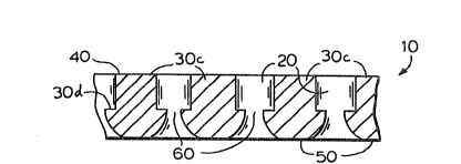
Fig. 3 is illustrative of a preferred
microsieve in accordance with this invention shown
generally at l0. As shown, the sides of apertures 20
are essentially vertical in contrast to the sloping
sidea of the apertures
1 30q6~39
1 in the prior art microsieve of Figs. l~a)-(c). This
arrangernent helps to lessen the opportunity for more than
one cell to occupy more than one aperture and also
minimizes distortion of the light path which can result in
apertures with comparatively gentle sloping walls.
Microsieve 10 of Fig. 3 is made by a
modification of the known method illustrated in Figs.
2(a)-(e). Specifically, instead of laying down a
thickness of photoresist 30 of only about 1 micron as in
Fig. 2(a), the thickness of the photoresist layer is made
to be about 7 microns or so. Thus, when the fixed areas
of photoresist are eventually removed to provide the
sieve, undercut areas 30(d) will actually have the
straight-bore configuration shown in Fig. 3. In use, the
undercut areas 30(d) of microsieve 10 face upwardly, i.e.,
toward upper face 40. At upper face 40, the diameter of
apertures 20 is about 6 microns and in the constricted
area 60, the diameter is about 2 microns; the diameter of
the opening at under surface 50 of microsieve 10 is of no
significance to the functioning of the device.
Microsieve 10 of Figs. 4(a)-(f) illustrates
still another embodiment of the present invention. As
shawn in Fig. 4(a), annular ~face 13a of rigid frame m~xr 13
which is fabricated from an electrically conductive
material such as copper, nickel, gold, silver, etc., is
placed against a suitable nonadherent surface 11, e.g.,
one which is substantially optically flat, either directly
thereon or indirectly upon a thin foil 12 which serves as
a shim to separate surface 13a a short distance,
e.g., 5 to 20 microns or so, from surface 11. Frame
member 13 possesses a relatively large aperture 14,
.... :
1 30q~q
1 preferably circular in configuration and defined within
the geometric center of s~rface 13a of the frame, filled
with a hardenable electrically conductive material 15,
e.g., Wood's alloy which solidifies below its melting
point of about 65C~ to form ~ smooth surface 17.
Electrical contact 16 is inserted before, during or after
hardening of electrically conductive material 15. Once
electrically conductive material 15 has become hardened,
i.e., by being cooled to below its solidification point,
it will possess a smooth surface 17 of electrically
conductive material corresponding to the configuration of
the large aperture 14.The sole function of surface 11 is to
provide corresponding surface 17 of the electrically
conductive material, when hardened, with a smooth,
striation-free surface and that of optional foil 12 to
extend surface 17 some short distance beyond surface 13a
of frame 13. After electrically conductive material 15
has hardened, surface 13a of frame 13 is removed from
contact with surface 11 and inverted to the face~up
position as shown in Fig. 4(b). In the latter figure/ a
layer of photoresist 18, e.g., of a photoemulsion or
photopolymerizable composition, is applied to surface 17
of electrically conductive material 15 and, for good
measure, to at least a part of surface 13a of frame 13 to
~re adequate and uniform coverage of the area which
will eventually be occupied by the array of apertures
constituting the microsieve. Typically, the height (or
thickness) of photoresist 18 will be on the order oE about
1 or 2 microns, the precise thickness being dependent in
large measure upon the rheological properties of the
particular photoresist selected.
~ 3"96~9
In Fig. 4(c), conventional masking/exposure
techniques (as described above in connection with Figs.
2(a)-(e) which are illustrative of the prior art)
provide a grid-like pattern o~ unexposed areas of
photoresist 18(a) surrounded by a continuous area of
exposed photoresist 18(b). Following conventional
developing, fixing and clearing operations, there are
provided the fixed areas of photoresist 18(a) supported
on Wood's metal 15 as shown in Fig. 4(d).
It will be understood that either positive or
negative photoresists can be used in the practice of the
invention in accordance with procedures which are well
known to those skilled in the art.
In the following step shown in Fig. 4~e), a
metal 19, e.g., copper, gold, silver, etc., is electro-
deposited upon the exposed surfaces of frame member 13
as in the known method of manufacturing a microsieve
described above. This electrodeposited metal 19
completely surrounds areas of fixed photoresistO As
sh~wn in Fig. 4(f), electrically conductive material 15
is removed from frame member 13, usually with only a
simple breaking-away action, and the fixed areas of
photoresist are removed by dissolution or etching with
an appropriate solvent to provide the finished,
completely self-supporting microsieve spanning what had
originally been large aperture 14 of frame member 13.
In the variation of the foregoing method
illustrated in Fig. 5, copper frame member 13' of
microsieve 10' initially does not possess an aperture.
However, an etchant resistant, electrically non-
conductive ~oating 24 is applied to the underside of
frame member 13' except for an exposed, bare copper
1 s'.~96'39
metal area 21 directly beneath the microsieve portion to
be formed from electroplated nickel 19' layer. An
etchant which selectively removes copper metal but which
does not affect nickel is then used to remove central
copper core 22 and fixed areas 18b~ of photoresist are
removed to provide a finished microsieve 10' similar to
that shown in Fig. 4(f).
In yet another variation of the method
described in Figs. 4(a) through 4(f) which is shown in
Fig. 6, central aperture 14 of frame member 13' is
filled with a readily meltable or solvent-soluble
electrically non-conductive material 30, e.g., a
paraffin wax, in place of electrically conductive
material 15 of Fig. 4(a). However, prior to applying
photoresist as shown in Fig. 4(b), an electrically
conductive metal 34, e.g., gold, silver, etc., is vapor
deposited upon the complete upper face of the frame
member to provide electroconductivity even in the area
of the aperture occluded by material 32. Thereafter,
the steps of applying photoresist, exposing, developing
and fixing the photoresist, washing exposed photoresist
away and electroplating metal are carried out as before.
Finally, material32 i5 removed, the exposed thin layer
of vapor deposited metal34 is selectively etched or
otherwise removed and the fixed arsas of photoresist are
removed to provide the finished microsieve 10'.
Another approach to imparting increased
rigidity to a microsieve is illustrated in Figs. 7(a)
and (b). Here, the object is to build up the thickness
of the microsieve body to the point where it becomes
appreciably more resistant to flex, yet without
1 3 6 ~) ~
sacrificing the numerical density of apertures.
As shown in Fig. 7~a), copper (or other
electrically conductive metal) mandrel 40 possesses
successive layers ~1 to 53 of electroplated metal, e.g.,
nickel, surrounding fixed photoresist areas 53b which
are in concentric alignment with the previously
deposited areas of photoresist therebeneath. This
method of manufacturing a microsieve requires that each
layer of electroplated metal be no higher, or thicker,
than the adjacent areas of fixed photoresist.
Optionally, all adjacent layers 41 to 53 can be
separated by a layer 54 of vapor deposited metal of only
a few angstroms thickness. With the removal of mandrel
40 and the fixed areas of photoresist 53b, there is
obtained the finished microsieve 60 shown in Fig. 7(b).
The foregoing method makes it possihle to vary
the cross-sectional geometry of the apertures from one
layer to the next and/or to stagger successive layers to
obtain an aperture with a non-vertical bore.
While various aspects of the invention have
been set forth by the drawings and the specification, it
is to be understood that the foregoing detailed
description is for illustration only and that various
changes in parts, as well as the substitution of
equivalent constituents for those shown and described,
may be made without departing from the spirit and scope
of the invention as set forth in appended claims.