Note: Descriptions are shown in the official language in which they were submitted.
13~7~7
SWITCHED-C~PACITOR CIRCUIT WITH LARGE TIME CONSTANT
Field of the Invention
The invention relates to the field of switched-capacitor circuits in
which the operating frequencies of interest are small in comparison to the clock5 speed operaeion of the circuits and in which, therefore, large capacitance ratios are
needed to realize the necessary large time constants required for operation.
Back~round of the Invention
The realization of very large time constant circuits (circuits which have a verylarge ratio between the operating clock ~requency and the pole/zero frequencies) is
10 a bottleneck in the design of many analog integrated circuits. Examples of this in
voice-band circuits are power supply rejeceion filters, such as 60 Hz/180 Hz notch
filters and automatic gain control loop filters which have pole frequencies of a few
Hz. The clock frequencies used for these filters are usually much higher, for
example, 128 KHz, as determined by the rest of the switched-capacitor circuitry in
15 the system.
The preferred technology for realizing switched chpacitor circuits has
been and is presently metal oxide semiconductor (MOS) technology. There have
been a number of solutions to the problem of designing such circuits using the
MOS technology. A paper eneitled "Switched-Capacitor Circuit Design" by
20 R. Gregorian et al., Proceedings f the IEEE, Vol. 71, August 1983, pp. 941-966,
surveys the field. In general, the realization of a MOS switched capacitor circuit
having a large integrating time constant is achieved by replacing the input resistor
of a conventional active RC integrator with a capacitive network that simulates a
resistance. One such network consists of two transistor switches serially
25 connected to an input of an operational amplifier and a capacitor connected from
the common point between the switches to ground. The two switches are operated
in different clock phases. The integrating time constant thus obtained depends
inversely on the operating clock frequency and proportionally on the ratio of the
integrating capacitance in shunt with the amplifier and the effective switched input
30 capacitance.
Lowering the clock frequency to achieve larger time constants in the
above circuit is not a viable alternative in many applications. Thus, the raeio of
integrating capacitance to input capacitance must be increased. Decreasing the
input capacitance to increase this ratio is not desirable because parasitic
35 capacitances then begin to play a dominant role. Thus, the integrating capacitance
muse be increased. This solution, however, requires large amounts of chip area.
~k
:L3~7~7
The problems of the above-described arrangement led to the use of the
now standard input T-capacitor network. This arrangement is discussed in a paperentitled "An Area-Efficient Approach to the Design of Very Large Time Constants
in Switched-Capacitor Integrators" by Sansen et al., IEEE Journal of Solid-State5 Circuits, Vol. SC-19, October 1984, pp. 772-779. The T-network approach has
the adYantage that it can easily be mixed with conventional switched-capacitor
circuitry. However, it suffers from a strong sensitivity to parasitic capacitances,
thus causing significant deviations in the time constant of the integrator. The high
parasitic sensitivity places constraints on the design and layout of circuits using
10 these integrators. This partially nullifies the area advantage of the technique.
Other known approaches for realizing very large time constants suffer
from more serious limitations. A method proposed by M. Yamamoto, "Large
Time-Constant SC Circuits and Uni-Value Capacitor SC Circuits Using Multi-
Phase Clock", Proceedin~s of the IEEE, International Symposium on Circuits and
15 Systems, May 1982, is parasitic-sensitive, apart from requiring a multi-phaseclock. An approach given by Viswanathan et al., "Increasing the Clock Frequency
of Switched-Capacitor Filters", Electronic Letters, Vol. 16, 1980, relies on
switching in more than two clock phases and does not yield simple circuits. Also,
the way the switching is performed between the separate functions of input
20 attenuation and integration results in an undes*able slewing of its output.
Summ~ry of the Invention
The above problems are solved, and an advance in the art is achieved
in an analog circuit comprising amplifying means, a switched capacitor network
connected betvveen a signal input and an input of the amplifying means and a
25 feedback capacitance connected between an output of the amplifying means and
the input to the amplifying means. The switched capacitor network includes a
sampling capacitance which is switched during a first clock phase to sample an
input signal and to transfer the resulting sample charge to the feedback
capacitance. D~uing a second clock phase, the sampling capacitance is switched
30 to withdraw the same charge from the feedback capacitance. The circuit further
includes a third capacitance which is switched in one of the clock phases to
acquire a charge from the output of the amplifying means and which is switched
in the other clock phase to distribute any charge acqu*ed during the one clock
phase with the feedback capacitance.
In the preferred embodiment, the sampling capacitance has one
connection to the input of the amplifying means and a second connec~ion switchedin the first clock phase to the signal input and switched in the second clock phase
J.Y'~
to a reference potential. The third capacitance is connected between the output of
the amplifying means and the reference potential during one of the clock phases
and is connected in parallel with the feedback capacitance during the other of the
clock phases.
S Brief Description of the Drawin~
FIG. 1 shows a prior a~t circuit using th.o T-network type of input
capacitance;
FIG. 2 shows an inverting integrating circuit built in accordance with
the principles of the invention;
FIG. 3 shows a non-inverting version of the circuit of FIG. 2;
FIG. 4 shows an exarnple of a lossy integrator using the principles of
the circuits of FIG. 2 and FIG. 3;
FIG. S shows an example of a notch filter using the principles of the
circuits of FIG. 2 and FIG. 3;
FIG. 6 shows a typical frequency response curve of the notch filter of
FIG.5; and
FIGS.7, 8 and 9 show examples of a low-pass biquadratic filter stage,
a band-pass biquadratic filter stage and a stage of a ladder circuit, respectively,
each using the principles of the circuits of FIG. 2 and FIG. 3.
Det~iled Description
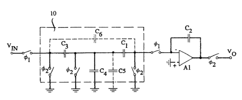
A conventional T-network 10 switched capacitor integrator is shown
in FIG. 1. Magnification of the ratio of the integrating capacitor C2 to the
effective input capacitance in this circuit is achieved by attenuating the input to
the integrator by means of the T-network cornprising the capacitors Cl, C3 and
25 C4. The designations ~1 and ~2 beside switches shown in this circuit indicate that
the respective switch is operated (closed) during the indicated clock phase ~1 or
~2- ~1 and ~ are mutually exclusive. That is, while ~1 is on, ~2 is off, and
vice versa. These same clock phase designations are used consistently in the
remaining figures.
It can be shown that the time constant of the integrator of FIG. 1 is
approximately given by:
~= 1 + Cl + C3 C4C2 (1)
C4 C4 C3C1fc
- 3 -
r~7 ~ 7
It is seen that the time constant is detelmined by the product of two
capacitor ratios C4/C3 and C2/Cl. This enables the realization of large time
constants with moderate capacitor ratios. However, this circuit suffers from a
strong sensitivity to parasitic capacitances. A parasitic capacitance Cs at the
5 Tjunction di}ectly affects the effective value of C4. A more senous problem
arises if there is any wiring parasitic capacitance between the bottom plates of C3
and Cl. This parasitic appears as a capacitor C6 in shunt with the small effective
capacitance generated by the T-network, thus causing significant deviations in the
time constant of the integrator.
The circuit schematic of an inverting integrator designed in
accordance with the principles of the invention is shown in FIG. 2. The operation
of this circuit is as follows. During a clock phase ~1, switch Sl is operated, an
input signal Vin is sampled by capacitor C3, and its resulting charge C3*Vin is
transferred to a feedback capacitor C2, Also, switch S3 is operated and the
15 resulting intermediate output voltage at the output of operational amplifier Al is
sampled by capacitor Cl. Thereafter, during clock phase ~2, switches S2 and S4
are operated, and Sl is opened causing C3 to withdraw the charge C3*V,r, from
C2~ During ~2, Cl distributes its charge with C2. Physically, this entire operation
is approximately equivalent to attenuating the input voltage Vjn by a
20 factor C3/C2, and then integrating it onto C2 through the capacitor Cl. Thus, the
capacitor C2 performs the dual functions of input attenuation and integration
without having to break the feedback loop around the amplifier Al. It can be
shown that the time constant of this integrator is approximately given by:
C2C
~ = (1 + Cl/C2) c C f t2)
Equation 2 shows that we can realize large time constants with
modest values for the capacitor ratios C2/CI and C2/C3. Moreover, this
integrator is insensitive to all parasitics to ground because every capacitor node
point is held at a nonfloating potential during every clock phase, as opposed to the
T-network of FIG. 1, for exarnple, where the common node between Cl, C3
30 and C4 is at a floating potential during ~1. Also, since the capacitor C3 of FIG. 2
is significantly larger than the small effective input capacitance of the T-network,
the circuit of FIG. 2 is less sensidve to wiring capacitance. The circuit is simpler
than the T-network integrator in terms of the number of capacitors and switches
More important, it is seen that both the ratios C2/Cl and C2/C`3 share the same
~ 3 ~ ~ 7 3 7
large capacitor C2, unlike in the T-network approach. This can result in a saving
of as much as 50% in total required capacitance.
The circuit schematic of a lossless non-inverting integrator, based on
the circuit of FIG. 2, is shown in FIG. 3. This circuit differs from the inverting
5 integrator of FIG. 2 only in the clock phases used to operate switches S3 and S4.
The invention can be extended to realize lossy integrators, as shown
in FIG. 4. A los~,y inverting integrator is obtained by using dle cl~ck phases
which are shown outside the parentheses in FIG. 4. A non-inverting lossy
integrator is obtained by using the clock phases shown inside the parentheses. In
10 addition to magnifying the ratio C2/C3 in accordance with the principles already
discussed, the ratio C2/C4 is also enhanced in accordance with the same inventive
principles, which is desirable in a lossy type of circuit. This is achieved by virtue
of the fact that the amplifier output is an input to C4 in the same way that theinput signal Vin is an input to C3. The transfer function of this integrator can be
15 shown to be:
1- Z-l + k--Cl C4 Z-
Cl C4
wherek = 1 +-- 1 +--
C2 C2
Equation 3 shows that a very low pole frequency can be achieved
without the need for very large capacitor ratios.
The integrators of FIGS. 2 through 4 can be used as generic building
blocks to realize a variety of switched-capacitor filters including first-order
sections, biquads and ladder realizations. The circuit schematic of one possibleimplementation of a notch filter, using the principles of the invention, is shown in
FIG. 5. Such a filter is generally employed as a power supply rejection filter in
25 analog systems. This circuit is based on the well-known E-type biquadratic
section. The E-type quadratic section is discussed in detail in an article entitled
"A Family of Active Switched-Capacitor Biquad Building Blocks" by
P. Fleisher et al. in the Bell System Technical Journal, Vol. 58. December 1979,pp. 2235-2269. A differential configuration has been chosen here because of the
30 particular application for which this filter was designed. A single-ended version
can be realized along the same lines. It is seen that the clock phases for the two
integrators I1 and I2 in the biquad are staggered. This is required because the
output of each integrator is valid only during one of the two clock phases.
- 5 -
13~7 3~
Similarly, in ladder structures using these integrators, the clock phases of theintegrators which form loops must be staggered.
A 60-Hz notch filter based on the configuration of FIG. 5 has been
designed to work with a clock frequency of 126 KHz. This filter has been
5 implemented in 1.5 micron CMOS. The filter uses 250 units (one unit=0.25 pf) of
capacitance, a significant saving over the T-network implementation which needs
about 325 units of capacitance. The chip area saving, in practice, is higher
because special design and layout constraints do not have to be used to overcomethe parasitic sensitivity of the T-network. The frequency response of this notch10 filter is shown in FIG. 6. Measurements on several samples showed a standard
deviation of 0.5% in the notch frequency. In contrast, T-network implementationshave often shown deviations in excess of 5%.
Other filter examples using the integrators of FIGS. 2 and 3 are shown
in FIGS. 7 through 9. Specifically, FIG. 7 shows a low-pass biquadratic filter
15 stage. This stage is based on the well-known E-type biquadratic topology
described in the above-cited Bell System Technical Journal. In particular, this
stage realizes the z-domain transfer function of the type
kz-
1 + az~l+ ~z-
where k, a and ~ are constants.
20FIG. 8 shows a band-pass biquadratic stage. This stage is also based
on the E-type biquadratic topology. It realizes the transfer function of the type
kZ-~ Z-l )
1 + az~l + ~z-2 -
FIG. 9 shows an integrating loop stage for a ladder filter. The loop
contains two integrators consisting of an inverting lossless integrator Il and a25 noninverting lossless integrator I2. Several such integrator loops may be
interlaced to form ladder filters of the types described in an article by
R. Gregorian, "Switched-Capacitor Circuit Design," Proc. IEEE, Vol. 71, pp. 941-966, August 1983.
It is to be understood that the above-described alTangements are
30 merely illustrative of the application of principles of the invention and that other
arrangements may be devised by workers skilled in the art without departing fromthe spirit and scope of the inventions.
- 6 -