Language selection

Search

Patent 1309758 Summary

Third-party information liability

Some of the information on this Web page has been provided by external sources. The Government of Canada is not responsible for the accuracy, reliability or currency of the information supplied by external sources. Users wishing to rely upon this information should consult directly with the source of the information. Content provided by external sources is not subject to official languages, privacy and accessibility requirements.

Claims and Abstract availability

Any discrepancies in the text and image of the Claims and Abstract are due to differing posting times. Text of the Claims and Abstract are posted:

  • At the time the application is open to public inspection;
  • At the time of issue of the patent (grant).
(12) Patent: (11) CA 1309758
(21) Application Number: 1309758
(54) English Title: COPPER THICK FILM MATERIAL SYSTEMS
(54) French Title: SYSTEMES DE MATERIAU CONDUCTEUR EN FILM EPAIS
Status: Expired and beyond the Period of Reversal
Bibliographic Data
(51) International Patent Classification (IPC):
  • H01C 17/06 (2006.01)
  • H01C 17/02 (2006.01)
  • H01C 17/065 (2006.01)
  • H01C 17/24 (2006.01)
  • H01C 17/28 (2006.01)
(72) Inventors :
  • OZAKI, THOMAS (United States of America)
(73) Owners :
  • GTE COMMUNICATION SYSTEMS CORPORATION
(71) Applicants :
  • GTE COMMUNICATION SYSTEMS CORPORATION (United States of America)
(74) Agent: R. WILLIAM WRAY & ASSOCIATES
(74) Associate agent:
(45) Issued: 1992-11-03
(22) Filed Date: 1988-08-24
Availability of licence: N/A
Dedicated to the Public: N/A
(25) Language of filing: English

Patent Cooperation Treaty (PCT): No

(30) Application Priority Data:
Application No. Country/Territory Date
090,192 (United States of America) 1987-08-27

Abstracts

English Abstract


THICK FILM MATERIAL SYSTEM
ABSTRACT
A material system for manufacturing thick film
resistors on a ceramic dielectric substrate is dis-
closed. The system includes the application and fixing
of resistor terminations composed of a precious conduc-
tor material to a dielectric substrate. Resistor
material is deposited over portions of the resistor
terminations and to the dielectric substrate intermedi-
ate the resistor terminations. Terminal pads, conductor
traces and resistor interconnections are printed on the
dielectric substrate using a base conductor material.
The resistor interconnections are deposited and fixed
to the resistor terminations and to portions of the
resistor material. The resistor material is trimmed to
tolerance by kerfing the resistor material and a
dielectric encapsulant is applied substantially over
the resistor interconnections and resistor material.


Claims

Note: Claims are shown in the official language in which they were submitted.

The embodiments of the invention in which an exclusive
property or privilege is claimed are defined as follows:-
1. A material system for manufacturing thick film
resistors on a ceramic dielectric substrate comprising:
at least first and second resistor terminations
located in a spaced relationship to one another and fixed
to said dielectric substrate, said resistor terminations
composed of a palladium - silver conductor material;
a ruthenium based resistive material fixed to
portions of said first and second terminations and to
said dielectric substrate;
at least first and second terminal pads fixed to
said dielectric substrate, and first and second conductor
traces extending from said first and second terminal pads
respectively to at least first and second resistor
interconnections respectively, said first and second
resistor interconnections fixed to said first and second
resistor terminations and to portions of said resistive
material, said first and second terminal pads, first and
second conductor traces and first and second resistor
interconnections composed of a copper conductor material;
and,
an infrared heat curable dielectric polymer
encapsulant applied and cured substantially over said
first and second resistor interconnections and resistive
material.
2. The material system for manufacturing thick film
resistors claimed in claim 1, wherein: said resistive
material is trimmed to tolerance before said encapsulant
is applied over said resistive material.
3. The material system for manufacturing thick film
resistors claimed in claim 2, wherein: said resistive
material is trimmed to tolerance by kerfing said resis-
tive material.

4. A material system for manufacturing thick film
resistors on a ceramic dielectric substrate comprising:
resistor terminations composed of a palladium -
silver conductor material fixed to said dielectric
substrate;
a ruthenium based resistor material fixed to por-
tions of said resistor terminations and to said dielec-
tric substrate;
terminal pads fixed to said dielectric substrate,
and conductor traces extending from said terminal pads to
resistor interconnections, said terminal pads, conductor
traces and resistor interconnections composed of a copper
conductor material, and said resistor interconnections
fixed to said resistor terminations and to portions of
said resistor material; and,
a dielectric polymer encapsulant applied and fixed
substantially over said resistor interconnections and
resistive material.
5. A material system for manufacturing thick film
resistors on a ceramic dielectric substrate comprising:
resistor terminations composed of a palladium -
silver conductor material fixed to said dielectric
substrate;
a ruthenium based resistor material fixed to por-
tions of said resistor terminations and to said dielec-
tric substrate;
terminal pads fixed to said dielectric substrate,
and conductor traces extending from said terminal pads to
resistor interconnections, said terminal pads, conductor
traces and resistor interconnections composed of a copper
conductor material, and said resistor interconnections
fixed to said resistor terminations and to portions of
said resistor material;
said resistor material is trimmed to tolerance; and,
an infrared head curable polymer encapsulant applied
and cured substantially over said resistor interconnec-
tions and resistor material.

6. The material system for manufacturing thick film
resistors claimed in claim 5, wherein: said resistor
material is trimmed to tolerance by kerfing said resistor
material.

Description

Note: Descriptions are shown in the official language in which they were submitted.


13~7~
THICK FILM MATERIAL SYSTEM
BACKGROUND OF THE INVENTION
This invention relates in general to the
manufacture of ceramic hybrid microcircuits and more
particularly to a novel material system for making
thick film resistors on a ceramic substrate.
Presen~ methods utilized in the manufacture
of the thick film resistors include a multi-stepped
process which builds the resistors and interconnects on
lo the substrate. This process first includes printing,
drying and firing of a conductor material, normally
palladium-silver (Pd-Ag), as pads, interconnects and
terminations. Then, a Ruthenium based resistor material
is printed on the substrate between the
palladium-silver pads. The deposited resistor material
is subsequently dried and fired. Next, a glass
encapsulant is printed, dried and fired over the
conductor pads and resistor. Finally, the the thick
film resistor is laser trimmed to tolerance.
The major disadvantage of the process outlined
above is material cost. Palladium-silver paste is
generally expensive. Further, since it is a precious
metal its cost is sub;ect to wild and rapid market
fluctuations. This price cost fluctuation provides
difficulty in pricing circuits and budgeting for
manufacturing cost.
The thick film industry has been searching
for an altsrnative to precious metal conductors and as
a result has developed base metal conductors, like
copper, which can provide conductors with greater
conductivity then with palladium-silver material.
However, base metal conductors must be fired in a
nitrogen atmosphere. Unfortunately, resistor paste
technology still required the use of air firing.
In order to make the conductor firing compat-
ible with the presently known resistor pastes, material
manufactures developed low temperature firing copper
~ *~

130~7~8
conductors which can be used with air fired resistor
technology. Air fired resistors compatible with the
copper conductor material are not compatible with any
nitrogen fired glass overcoats. Air fired overcoats
cannot be used since air firing will result in oxida-
tion of the copper film.
Encapsulants are required to provide long
term stability to the thick film resistors of less than
0.25% ohms, per 1000 hours, at 150 degrees c to 85
degrees C.
It therefor becomes an object of the present
invention to provide a novel thick film material system
for making thick film resistors using base metal
conductors and encapsulation.
SUMMARY OF THE INVENTION
In accomplishing the object of the present
invention there is provided a material system for
manufacturing thick film resistors on a ceramic
dielectric substrate.
The system includes the application and
fixing of resistor terminations composed of a precious
conductor material to the dielectric substrate. A
resistor material is then deposited over portions of
the resistor terminations and to the dielectric sub-
strate intermediate the resistor terminations.
Terminal pads, conductor traces and resistor
interconnections are then printed on the dielectric
substrate using a base conductor material. The resistor
interconnections are deposited and fixed to the resis-
tor terminations and to portions of the resistor
material.
Next, the resistor is trimmed to tolerance by
kerfing the resistor material and a dielectric
encapsulant is substantially applied over the resistor
interconnections and resistor material.

1 3 ~ ~ r~
BRIEF DESCRIPTION OF THE DRAWINGS
A better understanding of the invention may
be had from the consideration of the following detailed
description taken in conjunction with the accompanying
drawings in which:
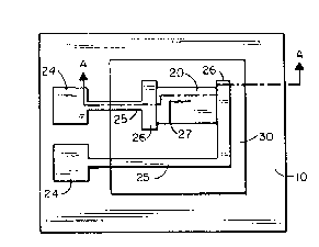
FIG. 1 is a top plan view of a thick film
resistor deposited on a substrate in accordance with
the present invention; and,
FIG.2 is a sectional view taken substantially
10 along line A-A of FIG. 1.
DESCRIPTION OF THE PREFERRED EMBODIMENT
Turning now to Fig~s 1 and 2 of the included
drawings the thick film material system of the present
15 invention will be explained. A pair of palladium-silver
(Pd-Ag) resistor terminations 12 are printed and dried
on a ceramic substrate 10. The terminations are then
fired in air at a temperature of 850 degrees C. A
Ruthenium based resi~tor material 20 such DUPONT R
20 1600, 1700 or 6300 series thick film resistor material
is printed over terminations 12. Portions of termina-
tions 12 are not covered by the resistor material 20 in
order to accept the conductor material of the next
step~ The printed resistor material is dried and fired
25 at 850 degrees C in air.
A layer of a base metal conductor, such as
copper, is printed on substrate 10 forming terminal
pads 24, and conductor runs 25. The copper conductor is
also applied over the resistor terminations 12 making a
30 conductive connection between the uncovered portions of
the resistor terminations 12 and the copper conductor
as shown at FIG. 2. The copper is then allowed to dry
and subsequently fired at 600 degrees C in nitrogen.
The now formed resistor is kerfed, shown as
35 27, using a laser to trim the resistor to tolerance.
A dielectric overglaze 30 is next printed
over the thick film resistor as shown. This overglaze

~3~7~
such as the MINICO M-70sO TM is polymer based and
curable using an infrared light source or conventional
oven at 200 degrees C in air. The polymer encapsulation
has advan~ageous over conventional glass encapsulation
in that moisture is not trapped within the encapsulant
during the curing process. The trapped moistUre leads
~o fluctuations in the ohmic value of the thick film
resistor. The infrared curable encapsulant allows for a
long term resistor stability of less than 0.25%, per
1000 hours, at 150 degree C to 85 degrees C.
Although the preferred embodiment of the
invention has been illustrated, and that form described
in detail, it will be readily apparent to those skilled
in the art that various modifications may be made
therein without departing from the spirit of the
invention or from the scope of the appended claims.

Representative Drawing
A single figure which represents the drawing illustrating the invention.
Administrative Status

2024-08-01:As part of the Next Generation Patents (NGP) transition, the Canadian Patents Database (CPD) now contains a more detailed Event History, which replicates the Event Log of our new back-office solution.

Please note that "Inactive:" events refers to events no longer in use in our new back-office solution.

For a clearer understanding of the status of the application/patent presented on this page, the site Disclaimer , as well as the definitions for Patent , Event History , Maintenance Fee  and Payment History  should be consulted.

Event History

Description Date
Inactive: IPC from MCD 2006-03-11
Time Limit for Reversal Expired 2001-11-05
Letter Sent 2000-11-03
Grant by Issuance 1992-11-03

Abandonment History

There is no abandonment history.

Fee History

Fee Type Anniversary Year Due Date Paid Date
MF (category 1, 5th anniv.) - standard 1997-11-03 1997-09-22
MF (category 1, 6th anniv.) - standard 1998-11-03 1998-09-14
MF (category 1, 7th anniv.) - standard 1999-11-03 1999-09-13
Owners on Record

Note: Records showing the ownership history in alphabetical order.

Current Owners on Record
GTE COMMUNICATION SYSTEMS CORPORATION
Past Owners on Record
THOMAS OZAKI
Past Owners that do not appear in the "Owners on Record" listing will appear in other documentation within the application.
Documents

To view selected files, please enter reCAPTCHA code :


To view images, click a link in the Document Description column. To download the documents, select one or more checkboxes in the first column and then click the "Download Selected in PDF format (Zip Archive)" or the "Download Selected as Single PDF" button.

List of published and non-published patent-specific documents on the CPD .

If you have any difficulty accessing content, you can call the Client Service Centre at 1-866-997-1936 or send them an e-mail at CIPO Client Service Centre.


Document
Description 
Date
(yyyy-mm-dd) 
Number of pages   Size of Image (KB) 
Abstract 1993-11-04 1 21
Claims 1993-11-04 3 85
Drawings 1993-11-04 1 17
Descriptions 1993-11-04 4 138
Representative drawing 2001-01-14 1 7
Maintenance Fee Notice 2000-12-03 1 178
Fees 1995-10-30 1 56
Fees 1996-10-27 1 55
Fees 1994-10-24 1 65