Une partie des informations de ce site Web a été fournie par des sources externes. Le gouvernement du Canada n'assume aucune responsabilité concernant la précision, l'actualité ou la fiabilité des informations fournies par les sources externes. Les utilisateurs qui désirent employer cette information devraient consulter directement la source des informations. Le contenu fourni par les sources externes n'est pas assujetti aux exigences sur les langues officielles, la protection des renseignements personnels et l'accessibilité.
L'apparition de différences dans le texte et l'image des Revendications et de l'Abrégé dépend du moment auquel le document est publié. Les textes des Revendications et de l'Abrégé sont affichés :
| (12) Brevet: | (11) CA 1309758 |
|---|---|
| (21) Numéro de la demande: | 1309758 |
| (54) Titre français: | SYSTEMES DE MATERIAU CONDUCTEUR EN FILM EPAIS |
| (54) Titre anglais: | COPPER THICK FILM MATERIAL SYSTEMS |
| Statut: | Périmé et au-delà du délai pour l’annulation |
| (51) Classification internationale des brevets (CIB): |
|
|---|---|
| (72) Inventeurs : |
|
| (73) Titulaires : |
|
| (71) Demandeurs : |
|
| (74) Agent: | R. WILLIAM WRAY & ASSOCIATES |
| (74) Co-agent: | |
| (45) Délivré: | 1992-11-03 |
| (22) Date de dépôt: | 1988-08-24 |
| Licence disponible: | S.O. |
| Cédé au domaine public: | S.O. |
| (25) Langue des documents déposés: | Anglais |
| Traité de coopération en matière de brevets (PCT): | Non |
|---|
| (30) Données de priorité de la demande: | ||||||
|---|---|---|---|---|---|---|
|
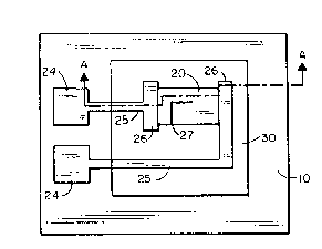
THICK FILM MATERIAL SYSTEM
ABSTRACT
A material system for manufacturing thick film
resistors on a ceramic dielectric substrate is dis-
closed. The system includes the application and fixing
of resistor terminations composed of a precious conduc-
tor material to a dielectric substrate. Resistor
material is deposited over portions of the resistor
terminations and to the dielectric substrate intermedi-
ate the resistor terminations. Terminal pads, conductor
traces and resistor interconnections are printed on the
dielectric substrate using a base conductor material.
The resistor interconnections are deposited and fixed
to the resistor terminations and to portions of the
resistor material. The resistor material is trimmed to
tolerance by kerfing the resistor material and a
dielectric encapsulant is applied substantially over
the resistor interconnections and resistor material.
Note : Les revendications sont présentées dans la langue officielle dans laquelle elles ont été soumises.
Note : Les descriptions sont présentées dans la langue officielle dans laquelle elles ont été soumises.
2024-08-01 : Dans le cadre de la transition vers les Brevets de nouvelle génération (BNG), la base de données sur les brevets canadiens (BDBC) contient désormais un Historique d'événement plus détaillé, qui reproduit le Journal des événements de notre nouvelle solution interne.
Veuillez noter que les événements débutant par « Inactive : » se réfèrent à des événements qui ne sont plus utilisés dans notre nouvelle solution interne.
Pour une meilleure compréhension de l'état de la demande ou brevet qui figure sur cette page, la rubrique Mise en garde , et les descriptions de Brevet , Historique d'événement , Taxes périodiques et Historique des paiements devraient être consultées.
| Description | Date |
|---|---|
| Inactive : CIB de MCD | 2006-03-11 |
| Inactive : CIB de MCD | 2006-03-11 |
| Inactive : CIB de MCD | 2006-03-11 |
| Inactive : CIB de MCD | 2006-03-11 |
| Le délai pour l'annulation est expiré | 2001-11-05 |
| Lettre envoyée | 2000-11-03 |
| Accordé par délivrance | 1992-11-03 |
Il n'y a pas d'historique d'abandonnement
| Type de taxes | Anniversaire | Échéance | Date payée |
|---|---|---|---|
| TM (catégorie 1, 5e anniv.) - générale | 1997-11-03 | 1997-09-22 | |
| TM (catégorie 1, 6e anniv.) - générale | 1998-11-03 | 1998-09-14 | |
| TM (catégorie 1, 7e anniv.) - générale | 1999-11-03 | 1999-09-13 |
Les titulaires actuels et antérieures au dossier sont affichés en ordre alphabétique.
| Titulaires actuels au dossier |
|---|
| GTE COMMUNICATION SYSTEMS CORPORATION |
| Titulaires antérieures au dossier |
|---|
| THOMAS OZAKI |

