Note: Descriptions are shown in the official language in which they were submitted.
~ ~(J97~1
. .
FR 9 87 014
IMPROVED REFERENCE VOLTAGE GENERATOR
FOR CMOS MEMORIES
The present invention relates to CMOS logic and memory
circuits, and is more particularly related to an improved
reference voltage generator for such circuits. As a matter
of fact, the generator of the present invention is
particularly suitable for the restore circuit of memories of
either the static type: Static Random Access Memories
(SR~1s) or dynamic type: Dynamic Random Access Memories
(DRAMs).
In SRAMs data is usually stored in cross coupled transistor
stages where one or more paths to ground can be selectively
switched on or off, while in DRAMs, data is stored in
capacitors by the operation of one or more transistors.
An access operation is performed in the same manner for both
types of memory, by discharging a path to ground.
A SRAM array comprises a matrix of static memory cells (MC),
interconnected with horizontal word lines t~L) and vertical
bit lines (BL). The memory cell is connected to the bit
lines through transfer gate transistors, the gate of which
is connected to the word line. Bit lines are common to all
oells located on one column, and constitute column busses
with a relatively high capacitance, due to the transmission
gate transistors connected in parallel. Read/write
operations are performed through these bit lines. Bits lines
are pre-charged high to a specific voltage level known as
the reference voltage, given by a reference voltage
generator thru a coupling circuit. In accessing the static
type cells, the cells selected through the word line decoder
transfer stored data to bit lines by partially discharging
the capacitance of one of the bit lines, thus developing a
differential voltage between the two bit lines connected to
a selected cell. This voltage difference is sensed by a
1 3~~q77 1
.. ..
~ r
FR 9 87 014
sense amplifier (SA) and amplified/latched in an appropriate
buffer, for subsequent outputting to input/output ~I/O) pads
of the SRP~ where desired.
, .
Thus, the next access to the array, can only occur after the
previously selected bit lines have been restored, to the
reference voltage. This operation i5 called "bit line
restore". The time required for this operation or "the
restore time", directly influences the cycle time, wh7ch is
the sum of the access time and the restore time. This
restore operation has therefore two disadvantages: first, it
increases the memory cycle time, because the restore and
access cannot overlap in time, and second it is necessary to
charge the bit lines which have a relatively high
capacitance.
In systems using dynamic memory cells which require
destructive read cycles, data is read from the memory cell
by detecting a voltage kick on the column bus as the
capacitor of the memory cell is either charged or discharged
when addressed.
Therefore there is a general problem in restoring highly
capacitive busses or lines in memory circuits. Same
reasoning also applies to logic circuits.
As far as SRA~Is are concerned, a typical solution is given
in the proceedings of the 1985 IEEE/SSCC Digest of Technical
papers pp 62-63 in an article entitled: "A 4.5 ns 256 K CMOS
SRAM with tri-level word line" by H. Shinohara et al , and
in particular in Fig. 2 which shows a circuit schematic of a
RAM including a standard restore circuit. Fig. 1 of the
present application is typical of such prior art schemes.
Fig. l is a schematic diagram of a circuit 10, which is a
portion of a conventional SRP~. Circuit 10 includes a
conventional static memory cell MCl which is part of an
1 30977 1
.. ..
~. r
FR 9 87 014
array of many such cells arranged in rows and columns in a
standard manner. Memory cell MCl is connected between two
bit lines: sL (true) and BL (inverted or complementary bit
line), which appear as column busses. Memory cell MCl is
addressed (i.e. enabled) by a row line or word line WL. The
latter therefore addresses all the memory cells in one row.
Transfer gate transistors mentioned above have not been
represented for sake of simplicity. Column busses or bit
lines BL and BL are respectively connected to the two arms
of a sense amplifier (not represented) as known in the art.
Bit lines BL and sL exhibit inherently high stray
capacitances referenced Cl and C2 resulting from paralleling
a great nu~ber of said transfer gate transistors which
increase with the number of cells in a column.
Circuit 10 also includes a restore circuit 11 for pulling up
the potential of bit lines BL and BL to the reference
voltage. Restore circuit 11 comprises two elementary
circuits: a coupling/equalizing circuit 12 and a reference
voltage generator 13. Circuit 12 comprises three P-channel
transistors P14, P15 and P16, connected between BL and BL,
and gated by bit line restore clock BLR. Transistors P14 and
P15 are used as coupling transistors. When turned on, they
apply the reference voltage available on the reference line
RL to the bit lines. On the other hand, the two bit lines sL
and BL are also coupled together through transistor P16, so
that the charge is equally shared between them. Thus,
capacitances Cl and C2 are both charged to the level of the
reference voltage. Transistor P16 therefore equalizes the
charge of capacitances Cl and C2 and therefore the potential
of the bit lines. Thus, transistors P14, P15 and P16
pre-charge the bit lines to the reference voltage, available
on reference line RL, during the restore time. In all
existing techniques known to the applicant, the reference
voltage qenerator 13 simply consists of a common N channel
transistor N17, the gate of which is connected to the drain
which, in turn, is connected to a first power supply VH.
1 309771
.. ..
., ,
FR 9 87 014
Transistor N17 operates as a standard static current source,
supplying the required current to high value capacitances C1
and C2, connected between the bit lines and a second power
supplyl in the present case, the ground GND. Transistor N17
is very large in size to avoid a considerable voltage drop
on the reference line during the restore time. The reference
potential is equal to VH-VT, VT being the threshold voltage
of transistor N17.
A conventional solution to the problem of restoring highly
capacitive bit lines to a defined reference voltage in a
SR~ involves the use of a very stable reference voltage
generator. This generator has to be very large to
accommodate the required current supply in the bit line
capacitances. Transistor Nl7 must then be designed large
enough to generate the adequate pre-charge level on the
memory bit lines. It is known to use a transistor with
several millimeters of channel width, e.g. 15 mm, and
therefore thls solution requires considerable space in the
design of modern silicon IC's.
If a smaller device were used, the designer would have to
reduce the speed of restoration, which would result in a
very long restore time. Generally, a compromise is made
between speed and space, which results in unsatisfactory
specifications.
The operation of the memory circuit shown in Fig. 1, with
transistor Nl7 making such a speed/size compromise will be
best understood with reference to the signal waveforms shown
ln Fig. 2, which illustrates the potential at various points
of circuit 10. Before memory cell MC1 is accessed, in the
initial state, reference line RL (curve 21, Fig. 2A), bit
line BL (curve 23, Fig. 2C) and complement bit line BL
(curve 24 for read operation, curve 25 for wrlte operation,
Fig. 2D) are all pre-charged to a level of one threshold
voltage below the power supply, say VH-VT. The bit line
1 30~771
FR 9 B7 014
restore clock BLR (curve 22, Fig. 2s)~ varies between VH and
GND (referenced 0). Following an access operation started
between times tl and t2, the potential of reference line RL
begins to drop at time t2, due to the current supply to the
bit lines.~At the same time t2, the bit line restore signal
BLR goes down to drive transistors P14 and P15, to provide
the current ~rom transistor N17 required to push up the
potential of the bit lines (BL and BL) to the reference
voltage VH-VT. The restore operation lasts from time t2 to
time t3. At time t3, the restore operation is considered
finished, all lines, and in particular the reference line,
are restored. Just after time t3, the BLR clock signal
rises.
In this solution, in which a trade off has been made, say
the size of transistor N17 is not large enough to be stable,
which means that a significant voltage drop in curve 21 is
tolerated, the standard restore time is about 12 ns.
In fact, the inherent "stability" of this classic voltage
source results in a speed disadvantage as it has to be made
excessively large. Because the current flow to charge the
bit line capacitances is always limited by design
constraints. Therefore, reference voltage generators of the
prior art are never perfectly stable, for that reason.
It is therefore a primary object of the present invention to
provide an improved reference voltage generator, with
reduced silicon area consumption and fast restoration of bit
line capacitances to a reference voltage.
In accordance with the broadest aspect of this invention,
there is provided an improved restore circuit for restoring
a highly capacitive bus to a reference voltage level less
than the nominal value of the power supply. It includes
coupling means connected between said bus and a reference
line where said reference voltage is available, said
1 3~977 1
FR 9 87 014
re~erence voltage being supplied by a reference voltage
generator. In the latter, according to the present
invention, the improvement consists of in that a dynamic
current source that is operated during the restore time is
added to the standard static current source.
The improved reference voltage generator is characterized by
two features : firstly the said static current source, which
still consists of a N MOS transistor operating as a resistor
load and connected between the reference line and a first
power supply, is significantly smaller. Secondly, the said
dynamic current source comprises a PMOS transistor, mounted
in parallel with the said N MOS transistor and gated so that
it conducts during the restore time.
In accordance with a more specific aspect of the present
invention limited to memory circuits, there is provided a
CMOS memory including a memory cell selected by an address
signal, at least one pair of bit lines for receiving/
transmitting a signal corresponding to information stored in
the said memory cell and a restore circuit for fastly
restoring of the bit lines to a reference voltage available
on a reference line, and including a reference voltage
generator consisting of a N channel transistor, the drain
and the gate of which are shorted and connected to a first
power supply. The improvement is characterized in that: the
said generator also includes a P channel transistor
connected between the reference line and the said first
power supply, and gated by a clock signal, which is timed by
the bit line restore clock, so that it will be activated
(turned ON) during the restore time.
According to that particular embodiment, the said reference
voltage is equal to one threshold voltage below the said
first power supply.
1 3~9771
~.
FR 9 87 014
The invention is therefore concerned with the combination of
the novel reference voltage generator with other circuitry
in memory systems using either static or dynamic type cells
and in loglc circuits as well.
The novel features believed to be characteristic of this
invention are set forth in the appended claims. The
invention itself, however, as well as other objects and
advantages thereof, may best be understood by reference to
the following detailed description of illustrated
embodiments, read in conjunction with the accompanying
drawings:
Fig.l is a schematic circuit diagram of a portion of a SRAM
having a conventional restore circuit including a standard
reference voltage generator.
.
Fig. 2 is a timing chart at dif~erent points of the circuit
shown in Fig. l.
Fig. 3A and 3B are schematic circuit diagram of the improved
reference voltage generator according to two preferred
embodiments of the present invention.
Fig. 4 is a timing chart at different points of the circuit
shown in Fig. 3, enabling the results obtained to be
compared with the conventional circuit shown in Fig. 1.
Fig. 5 is a schematic circuit diagram of a portion of a SRAM
having the improved reference voltage generator according to
another preferred embodiment.
Two versions of an improved voltage reference generator in
accordance with the present invention are shown in Figs. 3A
and 3B, and are respectively referenced by numerals 30 and
31. Comparing with voltage reference generator 13 in Fig. l,
the present invention mainly consists of the addition of a
1 30977 1
FR 9 87 014
very fast dynamic voltage source in addition to the standard
static current source device while significantly reducing
the size of the latter, for improved restore operation.
.
This very fast dynamic voltage source may be simply
implemented by an additional P channel transistor P33, the
size of which is 1/3 to 1/5 the size of N32. Transistor P33
is only activated during the restore time by a boost control
clock signal BCC, timed by the bit line restore BLR clock.
As the drain of this device is at a maximum of (VH-VT), it
operates in linear mode and quickly supplies additional
current I2 to the reference line RL. In addition,
transistor N32 is considerably smaller than transistor N17,
in Fig. 1, by a factor of about 10.
Voltage reference generator 30 could even be slightly
improved by connecting an additional transistor N34 between
the reference line RL and a second supply voltage GND as
shown in Fig. 3B. Transistor N34 is also a very small device
bleeding current to activate the reference voltage generator
31. It absorb~ any leak current generated by the circuit and
avoids any coupling of the reference line RL, the potential
of which might exceed VH-VT during the restore operation,
with the reference voltage generator.
Now turning to Fig. 4, the timing diagram shows the
potential at various points of the SRAM circuit of Fig. 1
when using the reference voltage generator shown in Fig.
3B. Operation is fairly similar to that of the circuit shown
in Fig. l. Before memory cell MC1 is accessed, in the
initial state, reference line RL (curve 41, Fig. 4A), the
bit line BL (curve 44, Fig. 4D) and the complement bit line
BL (curve 45 for read operation, Fig. 4D, curve 46 for write
operation, Fig. 4E) are pre-charged to the potential level
of the reference line (Fig. 4A) which is lower than power
supply voltage VH by the threshold voltage of transistor
N32, and therefore at VH-VT. The bit line restore clock
1 3~977 1
FR 9 87 014
(curve 42, Fig. 4s)~ and the sCc clock (curve 43, Fig. 4C)
vary between VH and GND.
Operation is quite similar to that described with reference
to Fig. 2. However, because transistor N32 is very small, at
time t'2, which is the beginning of the restore operation,
curve 41 shows a very sharp drop in the potential of the
reference line, caused by the discharge of the accumulated
charges in the bit line capacitances. At time t'3,
Transistor P33 operated by the BCC signal (curve 43),
provides a current I2, which in turn, compensates the drop
in current I1 supplied by transistor N32. Due to this
dynamic boost, the potential of reference line RL, see curve
41, fastly reaches VH at time t'4, and sets at the reference
voltage VH-VT shortly after time t'5. Time t'5 indicates the
end of the restore operation. With the improved reference
voltage generator of the present invention, restore times
down to 2-3 nsec have been obtained, which are considerably
less than when using previously known techniques, as
mentioned above.
In conclusion, the improved version of a restore circuit
according to the present invention, when applied to SRAMs,
pxovides significant performance improvements: the restore
time is reduced by a factor of three, and space required
consumed is reduced by a factor of ten.
The present reference voltage generator has been
successfully demonstrated with hardware. A prototype ran at
91MHz, for a 50 M~z design specification, and operated
perfectly on the machine.
Finally, the reference voltage generator of the present
invention is extremely versatile: various restore speeds and
various capacitive loads could easily be accommodated.
~ 3~977 ~
.:
FR g 87 014
As an example, depending on the desired restore speed, which
may differ according to Read or Write operations, or the
capacitive load to be driven (which in turn depends on the
size of the memory), transistor P33 may be adapted to be
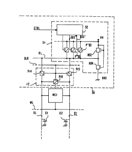
variable in size. The following design referenced 51 in Fig.
5 may be used. The circuit shown in Fig. 1 is the same
portion of a conventional SRAM, with a restore circuit 50
comprising a standard coupling/equalizing circuit 12 and the
improved reference voltage generator referenced 51,
according to further embodiment of the present invention.
Transistor P33, used in generators 30 and 31 (Fig. 3) is
replaced by a plurality of n P transistors: P'53,..., which
are all connected in parallel, and the gates of which, are
connected to the separate outputs of a programmable adder
52. Depending on the control signal CTRL, applied in input
to the adder, the desired number of P transistors in
parallel will be made active during the restore operation.
The static current source still comprises transistors N52
and N54.
Although the different embodiments of the invention
described above, concern to a P MOS transistor as an dynamic
current and a N MOS transistor as a static current source in
a C MOS memory device, the invention is also applicable to
MOS transistors with opposing conductivity.
In addition, the above concept, described with reference to
an application involving SRAMs, may be generalized to any
circuit design which requires restoration to a level less
than VH.