Note: Descriptions are shown in the official language in which they were submitted.
13~0~0
- ELEGTROSTATIC DISCHARGE PROTECTION NETWORK FOR
LARGE AREA TRANSDUCE~ ARRAYS
Field of the Invention
This invention relates generally to techniques and devices for protecting
large area transducer arrays, controlled by thin film transistor circuits, from
undesired high voltage effects resulting from electrostatic discharges and, in
10 particular, to equalizing the potential over all elements of the array during an electrostatic discharge event.
Background of the Invention
15 It is well known in the electronics industry that static electricity can cause
severe damage to IC devices. The generation of the electrostatic charge
results from the transfer of electrons within a body (polarization) or the
transfer of electrons from one body to another (conductive charging), and is
usually due to the interaction of bodies. The magnitude of the charge is
20 primarily dependent upon the size, shape, composition and electrical
properties of the substances which make up the bodies. The prime sources
of electrostatic charge encountered in a manufacturing facility are
essentially the interaction of personnel with insulators. Typically, walking
across a carpet, or over a vinyl floor, or the handling, rubbing or separating
25 various materials generates electrostatic charges which are transmitted to
the person and causes that person to be charged. When the charged person
handles or comes close to a susceptible electronic part, that part can be
damaged by direct discharge from the contact or by being subjected to the
electrostatic field surrounding the charged person. The generation of
5 15,000 volts between unprotected workers and electronic parts is not
unusual in a typical manufacturing facility.
In general, voltage sensitive parts fail due to dielectric breakdown of
insulating layers. In a transistor (MOSFET or TE`T) dielectric breakdown
10 usually occurs across the gate insulator. As feature sizes are reduced, in
order to increase the number of devices upon a single substrate, this scaling
makes the transistor more vulnerable to damage by smaller electrostatic
discharges. These discharges may cause catastrophic failure or may shift
the transistor operating characteristics out of specification. Failure results
15 when the dielectric strength is exceeded, causing insulator punchthrough
and leaving a low resistance short. The high potential difference across the
gate dielectric, caùsed by the presence of static charge, results in charges
being trapped in the dielectric and shielding the correct operational electric
field from the gate.
Numerous electrostatic discharge protection circuits have been developed to
protect the transistor gate dielectric against these high voltage effects.
These circuits usually are connected directly to the input contact pads and
serve to shunt away or reduce high voltage pulses to a value below the
25 critically disruptive valùe, while not interfering with device electrical
performance. Usually these protection networks include
diodes and other elements for which IC chip real estate
must be allocated.
It is an object of an aspect of the present invention to
provide a simple, low cost, electrostatic discharge
protection network for large area thin film transducer
arrays wherein each transducer has associated therewith
an addressing circuit including at least one thin film
transistor.
It is an object of an aspect of the present invention to
provide paths for potential equalization of all elements
on the array in response to spurious electrostatic
discharges.
SUN~aRY OF THE INVENTION
An aspect of the invention is as follows:
An electrostatic discharge protection network for a
large area transducer array, said array including a
substrate on which is formed a plurality of thin film
transducer elements and a thin film addressing circuit
associated with each transducer element for changing the
state of said transducer element, each of said
addressing circuits including at least one thin film
amorphous silicon transistor having a source terminal
electrode and a drain terminal electrode spaced from one
another and contiguous to a semiconductor layer, a gate
electrode spaced from said semiconductor layer by a gate
dielectric layer and located so as to control the
current flow from said source terminal electrode to said
drain terminal electrode, through said semiconductor
layer, and a plurality of input contact pads for
.~..~
131~
receiving external signals, connected to said
addressing circuit, for controlling the state of said
transducer elements said protection network including
a strip of n+ amorphous silicon resistive material
extending across all of said input contact pads, and
resistor means comprising inter contact pad portions of
said strip of resistive material for providing current
leakage paths to e~ualize the potential across all of
said gate dielectrics during an electrostatic discharge
and wherein said resistor means as connected to said
circuits and functioning to provide current leakage
paths does not affect the normal operation of said thin
film transistors.
By way of added explanation, the foregoing objects may
be achieved, in one form, by providing, upon an
insulating substrate, a large area thin film transducer
array in which each transducer has associated therewith
an addressing circuit for changing the state of the
transducer element, and wherein each addressing circuit
includes at least one thin film transistor having a
resistive path provided between the thin film transistor
gate electrode and one or both of the transistor's other
two terminal electrodes in order to provide current
leakage paths for equalizing the potential between the
gate electrode and the other two terminals during an
electrostatic discharge. The ohmic value of the
resistive path is selected to be large enough so that
current leakage between the gate electrode and
131 B~
,
the other two terminals does not affect the normal operation of the thin film
transis~or.
Brief Description of Drawings
The advantages of the present invention will be understood by those skilled
in the art through the following detailed description when taken in
conjunction with the accompanying drawingst in which:
10 Figure 1 shows a side elevation view of a thin fillm transistor,
Figure 2a schematically illustrates a thin film transistor wherein the gate
electrode is connected to both the source and drain terminal electrodes by
resistors,
Figure 2b schematically illustrates a thin film transistor wherein the gate
electrode is connected to the drain terminal electrode by a resistor,
Figure 2c schematically illustrates a thin film transistor wherein the gate
20 electrode is connected to the source terminal electrode by a resistor,
Figure 3 illustrates one embodiment of this invention on a large area one
dimensional transducer array,
. " .
~3~6~
Figure~ illustrates another embodiment of this invention on a large area
one dimensional transducer array,
5 Figure 5a illustrates this invention being practiced on a large area two
dimensional transducer array, and
Figure 5b illustrates the cross section of a liquid crystal display controlled by
the transducer array of Figure 5a.
Detailed Description of the Illustrated Embodiments
Turning now to the drawings there is illustrated the structure of a well
known amorphous silicon (a-Si:H~ thin film transistor (TET) 10, the so-called
15 inverted structure. It comprises a substrate 12 made of glass, ceramic, or any
other insulating material that remains adequately smooth and flat in the
common amorphous silicon TFT processing temperature range (<350C); a
gate electrode 14, typically 500 to 1000 angstroms thick formed by a thin
layer of Cr, NiCr or other suitable material, located on the substrate; a gate
20 dielectric 16, typically a silicon nitride layer several thousand angstroms
thick, overlying the gate electrode; an a-Si:H charge transport layer 18 a few
hundred to a few thousand angstroms thick; terminal electrodes formed of a
thin n~ a-Si:H layer 20 and an Al contact layer 22 about 1 micron thick
formed as the source 24 and the drain 26; and a second silicon nitride layer
1 3 ~
28 deposited over the a-Si:H layer in the channel region for passivation
purposes.
As between source 24 and drain 26, a current leakage path through the a-
5 Si:H semiconductor layer 18 exists when the gate of the transistor is not
connected to any voltage source, i.e., when the gate electrode is floating.
Therefore, during an electrostatic discharge to either the source electrode or
the drain electrode, the leakage path would allow the charge to move to the
other electrode, thus equalizing their potentials. Since virtually no current
10 can flow across the gate dielectric, electrostatic discharge to the gate
electrode could cause a large amount of charge to accumulate on the gate
electrode, thus generating an extremely large potential difference across the
gate dielectric between the gate electrode and either or both of the source
electrode and drain electrode. This is particularly true when the gate
16 electrode is floating and the accumulated electrostatic charges cannot be
drained away. Then the extremely large potential difference appearing
across the gate dielectric can cause the damage described.
To substantially minimize electrostatic discharge damage to the transistor
20 10, it is proposed to establish a high resistance current path connecting thegatel4 to the source 24 and/or the drain 26 by means of a resistor 30. The
alternative configurations are illustrated in Figures 2a, 2b and 2c. These
allow the potential to be equalized across the gate dielectric 16. In any of thethree cases care must be taken in selecting the proper value for the resistor.
25 By selecting a resistor whose value is too low the resistor pair (Figure 2a)
----6----
" ~
could thwart the proper operation of the TFI by bypassing the semiconductor
layer.-Alternatively, if the ohmic value is too high, the resistor will not
dissipate the electrostatic discharge fast enough to prevent damage to the
gate dielectric. As a general rule, the value of the resistor should be such
5 that the leakage current therethrough does not af~ect the proper operation of
the transducer element. The proper choice of the resistance value depends
upon the particular circuitry in each application.
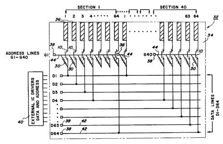
Turning to Figure 3 there is illustrated a one dimensional transducer array
10 32 in the form of a marking head of the type fully disclosed and described inUS 4,584,492. It includes a large area glass substrate 34 which has been
typically made eleven inches by three-quarters inch having thereon, along
one edge, marking electrodes 36, and along the opposite edge, input contact
pads 38 (more accurately illustrated in Figure 4, and only schematically
15 represented as bus lines in Figure 3). In use, the contact pads are connectedto receive marking information from external IC drivers 40. By means of a
multiplexed addressing arrangement, 104 input contact pads comprising 64
data lines 42 and 40 gate address lines 44 are sufficient for controlling 2560
marking electodes. Each of the gate address lines controls a section of 64
20 l~ rs 10, of the type described above. All of the elements, i.e. marking
elec'crodes, TFTsj address lines, data lines and input contact pads, are
integrally formed on the insulating substrate by thin film fabricating
techniques.
----7----
.
Whenthe array is not connected in a printing machine and is floating
electrically, as when it is being handled during testing, sorting, inspecting,
packaging and being installed in a printing machine, it is likely to make
5 contact with a body which carries an electrostatic charge. The electrostatic
charge which unsuspectedly has accumulated on an operator may be
released to the array and may destroy or damage one or more of the thin film
transistors, in the manner described above.
10 In order to protect each TFT, a resistor 30 is shown connected between each
gate electrode 14 and each source electrode 24. Depending upon the function
and arrangement of the transducer array it may be more desirable to connect
the gate electrode to either the drain electrode or to both the source electrodeand the drain electrode, as illustrated in Figure 2. By convention herein, the
16 terminal of the TFT which is connected directly to the transducer element is
identified as the drain electrode. In the transducer array of Figure 3 wherein
the transducers are marking electrodes 36 of the printer device described in
U.S. 4,584,592 and each marking electrode must hold the charge deposited
thereon for an entire line time, care must be taken to avoid establishing any
20 current leakage path between the drain electrode and the gate electrode.
Therefore, it would be undesirable to connect the drain electrode to the gate
electrode with resistor 30.
Although the Figure 3 embodiment will operate satisfactorily to protect the
25 TFTs from electrostatic discharge damage, it is not the optimum solution.
----8---
1310~0
This is because the resistors 30 take up valuable real estate which will be at
a premium when fabricating higher resolution marking head arrays. Also,
as the marking head arrays comprise more complex drive circuits, such as
those envisioned for multifunction operation, these drive circuits will include
5 several transistors associated with each marking electrode, and it would
become burdensome to provide a resistor for each transistor.
Therefore, rather than practicing this invention as shown in the Figure 3
embodiment, a much simpler approach is shown in the embodiment of Figure
10 4. The same result may be achieved by connecting all of the input contact
pads 38 extending along one edge of the marking head array 32 with a
resistive stripe 46 coextensive with the line of pads and in electrical contact
with them so as to form inter-contact pad resistors. This results in
connecting all the data lines 42 and all the gate address lines 44 so that
15 electrostatic charge accumulating on any one, or more, of these lines will
leak rapidly throughout the array and will equalize the potential on all
elements thereon.
The two major advantages of this configuration are: first, the resistive stripe
20 46 may be fabricated simultaneously with the deposition of the n+ a-Si:H
source and drain layers; and, second, that the resistive stripe is located on
the substrate at a location where it will not compete for real estate. It shouldbe understood that the resistive stripe may be fabricated of lightly doped or
undoped a-Si:H if desired, in order to be consistent with, and to be deposited
25 simultaneously with, other device layers. N+ a-Si:H is particularly
~ 3 ~
appealing because its resistivity is approximately 102
ohm-cm and in thin film form it is not uncommon to make
resistors in the range of 107 to 109 ohms.
Practical protective networks may be made with a
resistive strip whose inter-contact pad resistance is in
the range of 5 to 100 mega-ohms. The resistive value of
the inter-contact pad resistors must be selected to be
low enough to leak charge at a speed to prevent the
undesirable electrostatic discharge effects and high
enough so that during operation the voltage level on one
contact pad will not be significantly affected by
voltage levels on its neighboring contact pads. Since
the external IC chips used to drive the marking array
have a relatively low output impedance (on the order of
several kilo-ohms), there will be no significant cross-
talk between adjacent contact pads at different
voltages when adjacent contact pads are connected
together by these large inter-contact pad resistors (on
the order of several mega-ohms). Typically, the
resistance value should be greater than about ten times
the output impedance of the external drive circuit.
In U.S. Patent No. 4,719,481, issued January 12, 1988
~H.C. Tuan and M.J. Thompson) there is disclosed
transducer arrays in which each marking electrode
transducer element is controlled by an addressing
circuit comprising two thin film transistors. The
present invention, applied to that array, would protect
both TFTs from electrical discharges.
`~
~ 3 ~
The same approach to a protective network may also be used in the two
dimensional transducer array 48, shown in Figures 5a ant ~b. In this
embodiment, an orthogonal arrangement of display electrodes 50 is
5 deposited upon a large insulating substrate 52 so as to control the orientation
of liquid crystal material 64 in each pixel of a display panel 56. The state of
each display electrode is controlled by a TE~ 58. Each transistor receives a
data signal along a data line 60, connected to its source electrode 62, and an
address signal along gate line 64 connected to its gate electrode 66. When
10 the gate voltage turns the transistor ON current flows from the source
electrode 62 to the drain electrode 68 and then to the display electode 50. All
the source lines (Sl to SN) and all the gates lines (G1 to GN) are shown
connected together with suitable resistors, for example, n+ a-Si:H resistive
stripes 70. E~y following the principles of resistive value selection set forth
15 above, a protective network will be effected which will protect the gate
dielectrics of all the switching transistors from electrostatic discharge but
will have no effect on normal operation.
It should be understood that the present disclosure has been made only by
20 W8y of example and that numerous changes in details of construction and the
combination and arrangement of parts may be resorted to without departing
from the true spirit and the scope of the invention as hereinafter claimed.
2~
--11--