Note: Descriptions are shown in the official language in which they were submitted.
13101~
BACKGROUND OF THE INVENTION
Field of the Invention
The present invention relates generally to apparatus
for processing digital data and, more particularly, is
directed to an apparatus for processing digital data for use
with, for example, a so-called digital video tape recorder
to perform a reproducing operatic>n in a shuttle mode
(reproducing operation with a variable tape speed).
Description of the Prior Art
When a video signal is reproduced at variable tape
speed by a video tape recorder ~hereinater simply referred
to as a VTR) which reproduces data of one field by scanning
a plurality of tracks, a large timebase displacement or
timebase error occurs between a reference signal for the
reproduction and a reproduced signal. This timebase error
must be corrected.
Therefore, in the prior art, data and address are
extracted from reproduced data. Then, on the basis of the
thus extracted address, data is written in a memory, and-the
written data is read out therefrom on the basis of a read
address formed in response to a reference signal. The data
read out from the memory is subjected to a predetermined
signal processing such as an error detection, an error
correction and so on by an error detection/correction
circuit and then transmitted. An example of such a YT~
capable of playback at a variable tape speed is disclosed in
Japanese Patent Laid-Open Gazettes Nos. 56-144682 and
60-40573.
By the way, in the prior art digital data processing
apparatus mentioned above, data once written in the memory
-- 2
1 31~g
is held until new data will be written in the memory.
Accordingly, if there exists data of an address of the field
which is not reproduced during a long time of period because
of the reproducing operation with a variable tape speed
such as twice the normal tape speed, such data is held and
becomes data having no correlation with other portions of
the picture. Thus, such picture seems erroneous and the
motion of a real moving picture becomes poor so that a
residual image appears in the reproduced picture.
~O OBJECTS AND SUMMARY OF THE INVENTION
Accordingly, it is an object of this invention to
provide an improved apparatus for processing digital data
which can remove the above mentioned drawbacks.
It is another object of this invention to provide an
apparatus for processing digital data which can prevent
picture elements having no correlation from remaining even
upon playback at a variable tape speed.
It is a further object of this invention to provide an
apparatus for processing digital data which can improve a
follow-up property when a picture is moved or switched, so
that a residual image can be reduced.
~ ccording to one aspect of the present invention, there
is provided an apparatus for processing digital data
comprising:
a) an input circuit for receiving an input digital signal
including word data;
b) a write address generator for generating respective write
addresses associated with respective words of the word data
from the input circuit;
c) a first memory connected to the input circuit and for
-- 3
~31~ 8
storing the respective words of the word data from the input
circuit according to the respective write addresses;
d) a read address generator for generating respective read
addresses and for reading out the stored respective words
from respective addresses of the first memory according to
the respective read addresses;
e) an output circuit for deriving an output signal;
f) a word data generator for generating word data having a
predetermined pattern;
g) a switching member connected to the memory, to the output
circuit and to the word data generator and for selectively
providing the stored respective words from the first memory
or the word data having the predetermined pattern from the
word data generator; and
h) a controller connected to the write address generator and
the read address generator and supplied with the respective
write addresses and the read addresses so as to control the
switching member to provide the output circuit with the word
data having the predetermined pattern from the word data
generator instead of the stored respective words from the
first memory when same stored respective words are read out
predetermined multiple times.
These and other objects, features and advantages of the
present invention will become apparent from the following
detailed description of the preferred embodiment to be taken
in conjunction with the accompanying drawings, throughout
which like reference numerals identify like elements and
parts.
BRIEF DESCRIPTION OF THE DRAWINGS
Fig. 1 is a block diagram showing an embodiment of a
: - 4
': ~
1 3 ~ 8
recording system o~ a digital video tape recorder to which
the present invention is applied;
Fig. 2 is a schematic diagram showing an arrangement of
an outer code in an error correction code used in the
recording system shown in FigO l;
Fig. 3 is a schematic diagram showing an arrangement of
an inner code of the error correction code used in the
recording system shown in Fig. l;
Fig. 4 is a diagram showing a track pattern of recorded
tracks formed by the recording system shown in Fig. l;
Fig. 5 is a block diagram showing an embodiment of a
reproducing system of the digital video tape recorder to
which the present invention is applied; and
Fig. 6 is a block diagram showing a main portion of the
present invention.
DETAILED DESCRIPTION OF THE PREFERRED E~.BODIMENT
Now, an embodiment of an apparatus for processing
digital data according to the present invention will
hereinafter be described with reference to the attached -
drawings. In this embodiment, the present invention isapplied to a reproducing ~ystem of a so-called digital video
tape recorder (herinafter simply referred to as a digital
VTR), and processing circuits for processing an audio signal
and other signals are not described for simplicity because
they are not directly relating to the present invention.
Fig. 1 schematically illustrates a recording system 100
of a digital VTR to which the present invention is applied.
Referring to Fig. l, in the recording system 100, a
composite video signal of 255 llnes in one field is supplied
through a video signal input terminal 101 to an A/D
-- 5
~3~8~
(analog-to-digital~ converter 1~2, in which it ~s converted
into, for example, a sample of 8 ~its at a predetermined
sampling frequency. ~n this case, a television signal of,
for example, the NTSC system ~s sampled to form 768 samples
per line.
Sampled data o~ one field ~s sequentially divided into
3 segments in the vertical direction of the field, and
accordingly, one segment conta~ns data of 85 lines, or 65280
samples.
lQ In an inter sector shu~fling circuit 103, data of each
segment are scattered o~er two sectors so as to ~e arranged
in matrix ~or~ of 64 x 51Q samples in eac~ sector. The
data or 3264Q samples i~ tne sector tAus shu~fled are
supplied to an outer erro~ correction code encoder 1~4, in
which they are encoded ~nto data ~ith 4 parity words at
every outer cQde-bl~ck as shown in Fi~g. 2~
The thus arranged outer~coded data are shuffled ~y an
~ntra sector shuffling circui~ lQ5 and then supplied to a
mult~p~exer lQ7, in whic~ they~are added, in a time shaxing
2Q manner, with a sync~ Csynchro~izing~ signal and an ID
(ident~fy~ingl signal suppl~ed thereto from a sync. signal~ID
signal generat~ng ci~cuit lQ6 and thereafter encoded into an
inner er~or correctiQn code By an inner error correction
code en~oder lQ8 to form respecti~e sync. ~locks as shown in
Fig. 3~
As ~llustrated in ~ig~ 3~ one sync. block is formed of
2~yte synchxonizing dat~ SQI 51' a first inner code ~loc~
~xmed ~ 85-~yte data BQ tQ ~84 added with 2-~yte ID data
IDqr IDl and 8~yte inner parity check data K~ to K7, a
3Q second ~nner code ~loc~ of 85-by*e data Bo to B84 added with
0 8
8-byte inner parity check data Ko to K7. Then, 204 sync.
blocks constitute one video sector.
The thus arranged data is subjected to a code
modulation such as Modified Miller Code (M2 Code) by a
channel coding circuit 109, supplied through a recording
amplifier 110 and then recorded on a tape T by a plurality
of recording heads 111 mounted on a rotary head drum (not
shown) as shown in Fig. 4. In other words, one frame data
are recorded on 12 tracks and one video sector of 204 sync.
blocks is recorded on each track. Accordingly, the ID
signal shown in Fig. 3 contains the sync. block number and
the sector ID.
Fig. 5 illustrates a reproducing system 200 of the
digital VTR to which the present invention is applied.
Referring to Fig. 5, data reproduced from the tape T by a
reproducing head 201 is supplied through a playback
amplifier 202 to a channel decoding circuit 203, in which
the signal recorded according to, for example, the Modified
Miller Code is converted to a signal of an NRZ (Non Return
to Zero) modulation system and then ~ed to a sync. signal/ID
signal detecting circuit 20~. By the sync. signal/ID signal
detecting circuit 204, the sync. signal is detected to
thereby determine the sync. block and at the same time, the
ID signal is detected to thereby determine the signal
processing for each sampled data in the following signal
processing.
More particularly, since the ID signal contains the
sector ID and the sync. block number in the sector, if the
sequential order of respective samples within one sync.
block is judged, it is possible to determine absolute
-- 7
-` ~3~0108
addresses of the respective samples in the sync. block.
Therefore, from the sync. signal/ID signal detecting circuit
204, there are extracted the ~ideo data as well as the
addresses, each being corresponding to each of the video
data. ~ata supplied from the circuit 204 to an inner error
correction code decoding circuit 205 is subjected to the
error detection and correction processing by using the inner
code parity and the error of its ID signal is also detected.
If the error of such data can not be corrected, the address
of data of that sync. block is not reliable so that data of
such sync. block is not transferred to the next stage. If
the ID signal is correct and the error of video data is not
corrected, an error flag is added to the video data and then
transferred to the next stage.
The data subjected to the error correction process in
the inner error correction code decoding circuit 205 is
supplied together with the address to an intra sector
de-shuffling circuit 206, in which it is de-shuffled to data
arrangement of the outer code, which is then supplied to-an
outer error correction code decoding circuit 207. In the
outer error correction code decoding circuit 207, the error
correction processing is carried out with reference to the
error flag added by the inner error correction code decoding
circuit 205. Data, the error of which is not corrected
fully, is added with an error flag again and then supplied
to an inter sector de-shuffling circuit 208, in which it is
re-converted into the origianl data arrangement.
Thereafter, such error of the data added with the error flag
is concealed or interpolated by a known concealing or
interpolating technique in an error concealment circuit 209.
-- 8
-
~31~
The thus error-concealed or interpolated data is converted
into an analog video signal by a D/A (digital-to-analog)
converter 210 and then delivered through a video signal
output terminal 211.
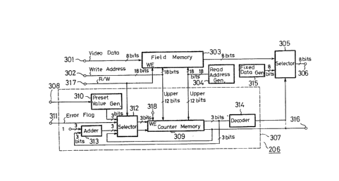
The intra sector de-shuffling circuit 206 shown in Fig.
5 will hereinafter be described ln greater detail with
reference to Fig. 6. Referring to Fig. 6, the video data of
8 bits delivered from the inner error correction code
decoding circuit 205 (Fig. 5) is supplied to a video data
input terminal 301 and written in a field memory 303 as a
first memory in response to a write address of 18 bits
applied thereto from an address data input terminal 302.
This write address is formed on the basis of the reproduced
ID signal in the preceding stage. The data written in the
field memory 303 is read out therefrom in response to a read
address of 18 bits generated from a read address generator
304 in such a manner that it is de-shuffled so as to return
to the intra sector shuffling. The data read out from the
field memory 303 is supplied through a selector 305, which
; 20 will be described later, to an output terminal 306 and then
transferred to the succeeding outer error correction code
decoding circuit 207 ~Fig. 5).
Further, the intra sector de-shuf~ling circuit 206 is
provided with a data hold timer circuit 307. In order that
the data hold timer circuit 307 operates only in a playback
mode with a variable tape speed, that is, a shuttle mode, a
variable speed playback signal is applied thereto through a
mQde signal input terminal 308. The data hold timer circuit
307 includes a counter memory 309 as a second memory and
upper 12 bits of the respective write and read addresses for
_ g
1 3 ~ 8
the field memory 303 are supplied to the counter memory 309.
Preset data of, for example, 3 bits generated from a
preset value generating circuit 310 and the error flag
applied to an error flag input terminal 311 from the inner
error correction code decoding circuit 205 (Fig. 5) are
supplied through a selector 312 to the counter memory 309 as
the inputs thereof. Alternatively, of the outputs derived
from the counter memory 309, timer count data of 3 bits is
incremented by one bit by an adder 313 and then supplied
through the selector 312 to the counter memory 309.
Of the outputs derived from the counter memory 30~, the
timer count data of 3 bits is also supplied to a decoder
314. When 3 bits of the timer count data all become "1", or
"7" in decimal notation, the decoder 314 generates a decoded
output to switch the selector 305 so that a predetermined
fixed data from a fixed video data generating circuit 315 is
delivered through the selector 305 to the video data output
terminal 306. On the other hand, the error flag derived
from the output of the counter memory 309 is ~ed back
through the selector 312 to the input of the counter memory
309 and is also supplied through an error flag output
terminal 316 to the succeeding outer error correction code
d~coding circuit 207 ~Fig. 5).
Subsequently, the operation of the data hold timer
circuit 307 will be described in association with the
operation of the intra sector de-shuffling circuit 206.
Upon playback mode with a variable tape speed ~or shuttle
mode), the magnetic head 201 traces the tape T across a
plurality of recorded tracks shown in Fig. 4 so that the
reproduced sync. blocks shown in Fig. 3 become skipped ones
.
-- 10
1 3 ~ 8
or discontinuous. Accordingly, data of one field is not
written in the field memory 303. ThereEore, the data
reproduced during one field period in view of time are
supplied to the inner error correction code decoding circuit
205 at the unit of the sync. block, in which they are
corrected for error and then written in the field memory 303
at the unit o~ inner code block during a period in which a
write enable signal is supplied to an input terminal 317.
The write address at this time is generated on the basis of
the ID signal added to each sync. block.
While, one of the addresses of the counter memory 309
is made to correspond to 85 addresses for 85 sampled data of
one inner code block in the field memory 303. To this end,
the upper 12 bits of the write address are supplied to the
counter memory 309 and the write enable signal applied to
the input terminal 317 is supplied to the selector 312 so
that the preset data of 3 bits indicative of, for example,
"0" from the preset value generating circuit 310 and the
error flag of the inner code block unit from the error flag
input terminal 311 are written in the counter memory 309 via
the selector 312. At that time, the write enable signal is
supplied through an input terminal 318 to the counter memory
309.
When the reproduced data of one field period is written
in the field memory 303, it is read out therefrom until
reproduced data of next field period is written therein.
The read address are derived from the read address
generating circuit 304 in such an order that not only the
addresses written in the preceding field period but also all
the field data are de-interlea~ed. At that time, the upper
1 3 ~ 8
12 bits of the read address are suppliecl to the counter
memory 309 and the read enable signal i5 supplied to the
input terminal 318 so that the timer count data and the
error flag are read out from the counter memory 309.
Accordingly, the video data read out from the field memory
303 is supplied through the selector 305 to the output
terminal 306 and the error flag associated with the video
data is transferred from the output terminal 316.
At the same time, the timer count data read out from
the counter memory 309 is supplied to the adder 313, in
which it is incremented by one bit and then supplied through
the selector 312 to the counter memory 309 thereby written
therein again. The error flag read out from the counter
memory 309 is fed back through the selector 312 to the
counter memory 309.
Accordingly, each time the video data of the same
address written once in the field memory 303 is read out
therefrom, the corresponding timer count data of the counter
memory 3~9 is incremented bit by bit. The timer count data
2~ read out from the counter memory 30g is supplied to the
decoder 314. When the timer count data becomes a value
indicating "7" in decimal notation, the switching signal i5
generated from the decoder 314 to switch the selector 3~5 in
such a manner that the selector 305 selects the i~ed video
data, for example, intermediate value data indicative of
"gray (grey) color" derived from the fixed data generating
circuit 315. This intermediate value data is transferred
through the output terminal 306. This output is supplied to
the succeeding outer error correction code decoding circuit
207 (Fig. 5). Alternatively, upon playback mode with a
- 12
~ 3 ~
variable tape speed, this output may not be subjected to the
outer code decoding but may be transferred directly.
Consequently, when ~he same data written once in the field
memory 303 is read out therefrom 7 times, such data i~
delivered in place of the fixed dataO In this case, if the
preset data i5 increased, it becomes possible to reduce the
number of the reading operations or the number of the
holding operations until the data is replaced with the fixed
data. In this case, also the preset value may be changed in
ganged relation with the reproducing mode. The incrementing
opera~ion for the timer count data i~ not carried out when
the data is read out from the field memory 303 but the
s incrementing operations may be carried out altogether during
the blanking period till the next field.
In the normal reproducing mode~ the above signal
! processing is not necessary because such a possibility isvery low that data, which is not reproduced during one
field, occurs. When a signal indicative of the normal
:t~
reproducing mode is supplied to the mode signal input
~~, 20 ~erminal 308, the pre~et value ~rom the prese~ value
generating circuit 310 is always set as -"6'l in the decimel
:. notation.
The data hold timer circuit 3~7 is not limited to the
above mentioned counter configuration but may take various
modifications such as a register configuration of multiple
stages. In this case, when the data are written in the
field memory tO3, corresponding addresses of the whole
stages of the registers are reset to "on. Then, each time
the same da' a is read out from the field memory 303, "1" is
sequentially written in the corresponding addresses of the
- 13
.,
131~1~8
respective stages of registers and it is detected that "1"
is written in the final stage of the register. Then, the
video data from the fie~d memory 303 is replaced by the
fixed data.
According to the present invention, as set forth above,
when the data are written in the first memory, the state
that the data are written therein in response to the
respective write addresses is stoxed in the second memory in
correspondence with the respective write addresses. Then,
when the data are read out from the first memory, the
corresponding read addresses of the second memory are made
to the state at the read-out and the data from the first
memory or the data from the other data source than the first
memory are delivered in response to the state of the second
; 15 memory. As a result, upon playback mode with the variable
tape speed, it is possible to prevent picture elements
having no correlation from remaining. Alsos when a picture
is moved or switched in the reproducing mode with a variable
tape speedj the follow-up property becomes excellent and a
residual image can be reduced very much so that a real
moving picture becomes excellent.
In the above-mentioned embodiment of Fig. 6, when the
output from the counter memory 309 reaches the predetermined
value, instead of the output data derived from the field
memory 303, the fixed data ~rom the ~ixed data generator 315
is transferred through the selector 305 by the output
derived from the decoder 314. However, instead of the above
arrangement, such a version is possible that, as indicated
by the broken line in Fig. 6, the output from the decoder
314 is transferred through the error flag output terminal 316
'
- 14 -
~ 3 ~
to the error concealment circuit 209 ~Fig. 5) as an error
flag. Then, this output can be concealed or interpolated
by the error concealmen~ circuit 209. In this case, it
becomes unnecessary to deliver th~e fixed data of the fixed
data generator 315 through the selector 305 to the output
terminal 3n6.
The above description is given on a single pre~erred
embodiment of the invention but it will be apparent that
many modifications and variations could be effected by one
skilled in the art without departing from the spirits or
scope of the novel concepts of the invention so that the
scope of the invention should be determined by the appended
claims only.
.
`:
~ 3Q