Note: Descriptions are shown in the official language in which they were submitted.
1310135
BUFFER MEMORY CONTROL APPARATUS
BACKGROUND OF THE INVENTION
The present invention relates to a buffer memory
control apparatus.
Such a circuit for controlling a buffer memory is
disclosed in U.S. Patent No. ~,332,010 and JP-B-57-57784 .
The latest large-sized and medium-sized electronic
computers generally employ a virtual storage system as well as
a buffer memory system. The virtual storage system is a
system in which a programmer can execute coding without being
conscious of the size of a real storage by working with a
logical address on a virtual storage not a real address on a
real storageO On the other hand, the buffer storage system is
a system in which a high-speed and small capacity buffer
storage is disposed in a main storage so as to stop a speed
gap in the main storage. A storage hierarchical structure is
thereby formed because the large capacity main storage is low
in processing speed in comparison with an operation speed of
the computer.
In a virtual storage system, it is necessary to
translate a logical address into a real addr~ss prior to
accessing the main storage. The translation of a logical
address into a real address is carried out by making reference
to an address translation table prepared in a program. If
such reference is made to the low speed main storage every
time translation is to be made, the reIative overhead time
necessary for the translation is great. In this regard, there
, . .
. .
2 131(~3~
is provided a translation lookaside buffer (hereinafter
abbreviated to "TLB"~ for storing pairs of logic address to
real address translations which have been obtained by making
reference to the main storage, so that when accessing the main
storage, a judgmsnt is made whether the logical address is in
question exists in the TLB or not prior to accessing. If the
logical address exists in the TLB (the probability of this
existence is very high because of locality of a program), the
real address corresponding to the logical address can be
obtained at a high speed from the TLB.
In the buffer storage system, on the other hand, the
buffer storage is a copy of a part of the main storage and
therefore a buffer address array (hereinafter abbreviated to
"BAA") is provided in the buffer storage in order to store the
correspondency between logical and real addresses. If a
central processing unit starts the main storage reference
with a logical address, a judgment is made as to whether a
real address corresponding to the logical address translated
by the TLB exists in the BAA or not so that when the real
address exists in the BAA (the probability of this existence
is very high because of locality of a program), necessary data
is read out from the buffer storage at a high speed and sent
to the central processing unit.
Although the above description has been made such
that the references to the TLB and BAA are made serially, it
is often necessary to make parallel reference to them in order
,
' '~ .
1 3 ~
to make the processing speed high. In this case, the BAA is
referred to with a logical address. There are however a
system in which BAA column identification is made with a real
address portion within a logical address or at an intra-page
address, and another system in which the identi~ication is
made with a logical address or an address including a part of
a page address to be subject to address translation. In the
latter system, there is an overlapping in bits of the
respective identification addresses to be given to the TLB and
BA~.
The present invention is applied to the latter
system.
It is an object of the preferred embodiment of the
present invention to provide a buf~er memory control apparatus
in which the above problems in the prior art are eli~inated to
thereby reduce the propagation delay as well as to reduce the
number of the input and output pins of the package.
It is another object of the preferred embodiment of
the present invention to provide a buffer memory control
apparatus in which it is made possible to read out and write
data corresponding to a given logical address from and into a
buffer memory at a high speed.
According to the preferred embodiment o~ the present
invention, each of TLBRA and BAA is divided into a plurality
of sections with respect to identification of logical
addresses in each column in such a manner that the logical
.
'` `~" "~` `
1310~L3S
addresses which are quite within the bounds of possibility of
simultaneous identification are stored in a region in which
transfer of information can be executed at a high speed, for
example, one and the same LSI.
According to the preferred embodiment of the present
invention, each pair of corresponding units of TLBRA and BAA
are incorporated in adjacent regions within one LSI, so that
it is possible to reduce the propagation delay as well as to
reduce the number of the input and output pins of the package.
Since each of the TLBRA and BAA is divided into a plurality of
sections with respect to identification logical addresses, it
is possible to attain the above reduction in the propagation
delay as well as in the pin number even if those TLBRA and BAA
are large in their capacity.
In accordance with one aspect of the invention there
is provided a buffer memory control apparatus comprising: an
address register for holding a logical address, the logical
address having a first group of bits, a second group of bits,
and a third group of bits, the groups being mutually exclusive
of each other; a buffer storage memory for storing a part of
information stored in a main storage, the buffer storage
memory being addressable by a combination of the first and
second groups of bits; a buffer address array for storing
first real addresses of data blocks stored in said buffer
memory; a translation lookaside buffer for translating the
logical address into a one of other first real addresses when
an access request is made by said logical address, the
translation lookaside buffer being addressable by a
.
13~35
s
combination of the second and third groups of bits; a
plurality of real address storage portions provided in said
translation lookaside buffer for storing second real addresses
in columns of said plurality of real address storage portions,
each real address storage portion :being addressable by a
combination of the first group of bits and a part of the
second group of bits; a plurality of buffer storage address
sub-arrays provided in said buffer address array in such a
manner that said plurality of buff~er address sub-arrays are
equal in number to said plurality of real address storage
portions, for storing the first real addresses in columns,
each of said plurality of buffer address sub-arrays bei.ng
addressed by a combination of the first group of bits and a
part of the second group of bits and being combined with said
real address storage portions correspondingly and respectively
to thereby form combinations of said real address storage
portions and said buffer address sub-arrays, each combination
being formed on a common LSI chip; a plurality of comparator
means, each disposed correspondingly and respectively to said
combinations of said real address storage portions and said
buffer address sub-arrays, each for detection of coincidence
between a second real address obtained by translating the
logical address for which the access request is made by using
said address translation lookaside buffer, and a first real
address stored in said buffer address array, each of the
~ 3 ~
comparator means being formed on said LSI chip common to the
combination; and selection means for selecting one of the
comparison results from a plurality of LSI chips based on the
remaining part of the second group of bits.
BRIEF DESCRIPTION OF THE DRAWINGS
Fig. 1 is a block diagram of a buffer memory control
apparatus;
Fig. 2 is a block diagram illustrating a structure
of a bipolar memory; and
Fig. 3 is a block diagram illustrating an embodiment
of the buffer memory control apparatus according to the
present invention.
Fig. l is a block diagram showing a part of a buffer
storage device of the system in which reference is made to the
above-mentioned TLB and BA~ parallelly. Upon generation of a
memory request from a central processing unit, a logical
address is stored in a register 91. The entry of the logical
address in a TLB 92 is identified by a lower bit b of an
upper-rank page address of the logical address. In this
example, the TLB 92 is composed of k columns x 2 rows, and the
reference numerals 92-1 and 92-2 represent first and second
rows respectively. That is, each of the first and second rows
has k entries. Each entry in each of the first and second
rows 92-1 and 92-2 of the TLB 92 is composed of a logical
address portion (L), a validity flag bit portion (V), and a
real address portion (R~. The logical address portion and
13~3~
real address portion of the TLB are called TLBLA and TLBRA
respectively. The contents of the portions L and V read out
from each row of the TLB 92 are compared with an upper bit a
of the page address in the register 91 by corresponding
logical address comparators 94-l and 94-2 respectively.
The BAA is identified with an upper bit c of a lower
rank intra-page address of a virtual address. In this
embodiment, the BAA 93 is composed of e columns x 2 rows and
the reference numerals 93-1 and 93-2 represent first and
second rows respectively. That is, each row has e entries.
Each entry of the BAA 93 is composed of a real address portion
(R) and a validity flag bit portion (V). Real address
comparators 96-1 and 96-2 compare a real address (intra-page
address or displacement) read out from the portion R of the
TLB 92-1 and entered through a selector 95 or a real address
(intra-page address or displacement) directly stored in the
register 91 by the central processing unit, with the contents
read out from the portion R of the corresponding row 93-l or
93-2 of the BAA 93. The selector g5 is arranged to select the
contents of the register 91 when the central processing unit
has stored a real address directly in the register 91, or
select the contents of the row 92-1 of the TLB 92 whe~ a
logical address has been stored in the register 91. Other
comparators 97-1 and 97 2 are arranged to compare the real
address read out from the portion R of the row 92-2 of the TLB
92 with the real address read out from the portion R of the
~ ' ,
.
, ' ' ~ ' ' .
~3~3~
corresponding rows 93-1 and 93 2 of the BAA 93. Upon
detection of incidence between the two inputs, the output of
each of the real address comparators 96-1, 96-2, 97-1 and 97-2
becomes "1".
The results of comparison by the real address
comparators 96-1, 96-2, 97-1 and 97-2 are entered into an
encoder 98, and after selected, an encoded output (one bit in
this example) of the encoder 98 is stored in a upper bit of a
register 99. An intra~page address of the register 91 is
stored in a lower bit of the register 99. Thus, a buffer
storage address corresponding to the logical address or real
address stored in the register 91 is obtained. A buffer
storage is identified with this address of the register 99 and
the data thus read out from the buffer storage is transferred
to the central processing unit.
Requiring a high speed property as well as a certain ?
capacity, the TLB 92 and BAA 93 are generally constituted by
bipolar memories. Fig. 2 shows a bipolar memory to be used
for such a purpose.
In Fig. 2, after decoded in an X-address decoder 110
and a Y-address decoder 114, address signals applied to input
pins Ao - A~ and A3 - A~ of ths X- and Y-address decoders 110
and 114 actuate a memory cell 112 through drivers 111 and 113
respectively. In this example, the memory cell 112 is
composed of 8 x 8 bits, that is, 64 bits. A selected one bit
of the memory cell 112 is led to an output cir¢uit 116 through
a sense amplifier 115. ~he mode becomes a write mode when an
input NE (write enable) is ~alid. In the write mode, an input
1~
.
- " ''.
. ., - ' :
- . :. :
~31~3~
DI (data-in) is passed through a gate 117 so as to be ANDed
with the WE in an AND 118 and another AND 119. Write "1" or
Write "O" is made valid by the outputs of the ANDs 118 and 119
so as to gi~e write instructions, through the driver 113, to
the bit of the memory cell 112 designated through the address
inputs Ao - As~
When used as the aforementioned TLB or BAA, the
bipolar memories of the kind as described above are arranged
in the form of a matrix to thereby reali~e a desired word
length as well as a desired bit length.
The recent development and improvement of extra high
density LSIs has begun to make it possible to realize making
electronic computers large in scale and high in processing
speed. This tendency will likely be promoted from now on.
Thus, logical devices such as operation devices have come to
be made of LSIs and to be made high in processing speed. on
the othar hand, however, the possibility exists that logical
portions including bipolar memories may become a critical path
which limits a machine cycls in an electronic computer because
most parts of the logical portions are occupied by gates which
are used to increase addressing to tha bipolar memories and to
decrease the number of dat~ readings from the bipolar
memories, so that it i5 difficult to constitute the logical
portions by LSIs and therefore impossible to make the best use
o~ such LSIs. Further, there is a tendency that a main
storage becomes large in its capacity and therefore it is
required to make the capacity of a buffer storage large. That
is, it is required to increase the BAA capacity. On the other
. ' ' ''' ~ .
,
'
1 3 ~ 3
hand, the technique to make bipolar memories highly integrated
has been promoted so that it has become possible to realize
high speed memories. However, it is not easy to realize a
structure of a large capacity BAA by using bipolar memories
having such a structure as described above with respect to
Fig. 2, because it is required to extremely increase the
number of package pins of the bipolar memories.
For example, in the case where a 4K-bit memory is
composed of 64 words, each word can accommodate 64 bits,
however, about 140 pins are required for address lines, data
lines, control lines, and power supply lines, so that the
package size of the bipolar memory is limited by the number o~
those input and output pins.
The above JP-B-57-57784 discloses a device in which
a TLB and a BAA are constituted by memories of the type in
which comparators are included in an LSI for the BAA. For
example, in the JP-B-57-57784, it is intended to solve the
above problems by making the portions encircled by broken
lines in Fig. 1 be incorporated in a memory chip.
In the above JP-B-57-57784, a real address read out
from the TLB is once led to the outside and then entered into
the memory chip constituting the ~AA so that the real address
is co~pared with a real address read out from the BAA. There
is therefore a problem that the nu~oer o~ pins required for
input and output of the TLB and BAA increases and propagation
delay also increases. There is a further problem that the
, ~ :
- -
- ~'' . ' ' ~ " '
.. , ~ '- .
~3~ ~3~3
11
communication path among the TLB, BAA, comparators provided in
a single LSI becomes so long that the signalling time among
those elements is prolonged.
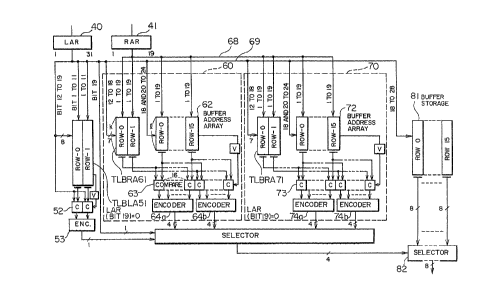
Referring to Fig. 3, an embodiment of the present
invention will be described in detail here~mder, In the
drawing, the numerals 1-31 attached to devices designate
address bit positions and the numerals attached to lines
designate the number of signal bits. Each region
rectangularly encircled by a broken line is a region in which
transfer of information can be made at a high speed. For
example, one LSI may be such a region, which is represented as
an LSI 60 and an LSI 70 in the following. The reference
numerals 40 and more are used to designate other constituent
parts.
In Fig. 3, a logical address for instruction fetch
or operand fetch is set in a logical address register ~AR 40.
The logical address is composed of 31 bits from bit 1 to bit
31. In an address translation buffer (TLB, 51, 61, 71), the
directory of the entries registered in the TLB is abbreviated
20 to TLBLA, and a data portion in which real addresses are
stored is abbreviaked to TLBRA. ~ buffer address array for
holding real addresses of the data held in a buffer memory is
i abbreviated to BAA and the buffer memory is abbreviated to BS.
The logical address set in the LAR 40 is used to
make an access to the TLB, the BAA, and the BS. The TLB has
two rows the columns of which are identi~ied with the bits
12 - 19 of the logical address, while the BAA has 16 rows
which are identified with the bits 18 ~ 24 of the logical
~3~.3~
12
address. Data of 16 rows are read out ~rom the BS 81 and one
of the data can be selected at a high speed if the TLBRA and
BAA can be stored in one and the same LSI (with no inter-IC
connection). If the TLBRA and BAA cannot be stored in one and
the same LSI, it is necessary to divide the TLBRA and BAA into
a plurality of sections so as to store the TLBRA and BAA in a
plurality of LSIs. The present invention is intended to show
a manner how to di~ide the T~BRA and BAA.
In this embodiment, since the column identification
addresses of the respective TLBRA and BAA which are common or
overlapped at the bits 18 and l9 and the columns of the
respective TLBRA and BAA which are different from each other
at these bits 18 and 19 are not identified at the same time,
the TLB~A and BAA can be divided so as to obtain four
combinations. In Fig. 3, each o~ the TLBRA and BAA is divided
into two sections. Depending on the state of the bit 19,
whether it is "1" or "0", the sections are identified for a
specific LSI~ In particular, when the bit l9 o~ each is
identi~ied with "0", tha address is stored in the LSI 60 and
sections 61 and 62 of the respective TLBRA and BAA are used,
when the bit 19 of each is identified with ~ , the address is
stored in the LSI 70 and section 71 and 72 o~ the TLBRA and
BAA are used. An address bit line 69 from the LAR 40 is
supplied to both the LSIs 60 and 70. The T1BRA sections 61
and 71 are identified with the logical address bits 12 - 18,
while the BAA sections 62 and 72 are identified with the
logical address bits 18, and 20 - 24. Read out real addresses
are compared by comparators 63 and 73, and upon coincidence
, . ,: .
' ~ , .
,
~ 3 ~
13
the respective row numbers are encoded in encoders 64a, 64b,
74a and 74b. One of the respective outputs of the encoders
64a, 64b, 74a and 74b is selected by a selector 80 in
accordance with the combination of the value of the bit l9 of
the logical address set in the LAR 40 and the value of the
output of an encoder 53. When the value of the bit l9 o~ the
logical address set in the LAR 40 is "0", the respective
outputs of the encoders 74a and 74b are made invalid while
when it is "l" the respective outputs of the encoders 64a and
64b are made invalid. When the TLBLA coincidence signal put
out from the encoder 53 indicates the row 0, the respective
outputs of the encoders 64b and 74b are made invalid, while
when the TLBLA coincidence signal indicates the row 1, the
respective outputs of the encoders 64a and 74a are made
invalid. In response to the BAA coincidence signal selected
by the selector 80, a selector 82 selects ona of the 16 rows
of outputs of the BS 81 and puts out the same as data o~ 8
bites.
Fig~ 3 shows a buffer memory control apparatus for
instruction fetch or operand fetch. Also in the case of
operand store, a circuit for iudging into which one of the 16
rows of the BS 81 an operand is to be written is constituted
on the basis of similar point of view to that described above.
Further, when the logical address set in the LAR 40 has not
been registered in the ~LB, a real address corresponding to
the logical address is obtained by well known means, the thus
obtained real address is set in a real address register 4l
(hereinafter abbreviated to 'IRAR"), and after determination of
,"., ~ , .
: '
3 ~
14
a row to be replaced by, for example, a least recently used
(LRU) algorithm or the like, the bits 1 - 11 o~ the logical
address are stored in that row of the column of the TLBLA 51
designated by the bits 12 - 19 of the logical address and the
bits 1 - 19 of the real address sel: in the RAR 41 are stored
in that row of the column of the TLBRA section 61 designated ?
by the bits 12 - 18 of the logical address when the bit 19 of
the logical address is "0" while stored in that row of the
column of the TLBRA section 71 des:ignated by the bits 12 - 18
of the logical address when the bit 19 of the logical address
is "1". An address bit line 68 from the RAR 41 is supplied to
both the LSIs corresponding to the bit line 69.
When a blocX designated by a logical address set in
the LAR 40 has not been registered in the BAA, the logical
address is translated into a corresponding real address by
using the TLB, the thus obtained real address is set in the
RAR 41, and after determination of a row to be replaced by,
for example, an LRU algorithm or the like, the bits 1 - 19 of
the real address set in the ~AR 41 are stored in that row o~
the column of the BAA section 62 designated by the bits 18 and
20 - 24 of the logical address when the bit 19 of tbe logical
address is "0". They are stored in that row of the column of
the BAA section 72 designated by the bits 18 and 20 - 24 of
the logical address when the bit 19 of the logical address is
"l". A block designated by the logical address set in the LAR
40 is transferred to and stored in the BS 81.
'~'
- ~
.