Note: Descriptions are shown in the official language in which they were submitted.
131~1~3~
SIJRFACE MOUNT TECHNOLOGY BREAKAWAY
SELF REFULATING TEMPERATURE HEATER
. _
The present invention relates to an improved method
and apparatus for soldering individual terminals of a
surface mount connector to respective contact pads
disposed on a surface of a printed circuit board.
Although the description set forth below specifies solder
as the joining material, it is to be understood that any
fusible electrically conductive material, such as doped
conductive plastic material, may be employed.
Connectors having terminals with solder tails
extending therefrom for reception in plated through holes
of a printed circuit board are well-known. Relatively
recently, in the interests of facilitating automated
contact placement and economy of circuit board
manufacture, surface mount connectors have been developed
with terminals having solder tails formed for disposition
against respective plated contact pads on the surface of
the board. The terminals are typically fixed in the
connector housing, and the tails are formed to su~ficient
length to assure compliance with the pads regardless of
any tendency of the board to warp. Typically, each solder
tail is individually manually soldered to a respective
contact pad by any of a variety of known techniques. The
repetitive soldering operations are both time consuming
and costly.
14323 CA
3 ~
There have been a number of prior art attempts to
automatically solder multiple conductors, such as solder
tails of a surface mount connector, to respective contact
pads on a printed circuit board. In this regard reference
is made to U.S. Patent No. 4,484,704 (Grassauer et al) and
the prior art described therein. In the Grassauer patent
and other prior art soldering procedures for forming
multiple solder joints simultaneously, a soldering tool is
employed to deliver the necessary thermal energy over a
large continuous area spanning all of the connection
sites. Upon energization, the soldering tool heats up
until it overshoots a control temperature before settling
down to that temperature. The control temperature is
typically chosen somewhat above the ideal soldaring
temperature in order to compensate for less than ideal
thermal energy transfer. This approach to thermal energy
delivery has a number of disadvantagesO One such
disadvantage is damage to components resulting from
overheating. For example, the thermal overshoot inherent
in the heating tool can damage components disposed between
the connection sites within the area heated by the tool.
In some cases the overshoot may cause damage to the
poiymeric materials, insulating materials and adhesives at
the connection site. It is tempting to suggest that the
operator of the soldering tool might avoid the thermal
overshoot by either removing the tool before the overshoot
14323 CA -2-
~ 3 11 ~
occurs or delaying application of the tool until after the
overshoot occurs. This is impractical for a number of
reasons. First, there is no evident indication as to when
the thermal overshoot occurs. Second, although the tool
warm-up time is relatively long, the time interval during
which the tool temperature is sufficient to melt solder,
but prior to overshoot, is too short to reliably complete
the soldering operation. Further, where the tool is also
employed to apply pressure to the connection site, the
power must be turned off after the solder melts while
pressure is maintained on the tool until the solder
solidifies. The tool must be re-energized to effect the
next soldering cycle. These repeated on-off cycles change
the starting temperature for the transient overshoot in
each cycle, thereby making it virtually impossible to
determine when the tool attains the final control
temperature.
Another problem associated with prior art techniques
for simultaneously ~oining multiple solder tails of a
surface mount connector to respective contact pads of a
printed circuit board relates to positional alignment of
the components during soldering. It is not only necessary
for the multiple solder tails to be simultaneously aligned
with respective multiple contact pads on the printed
circuit board surface; in addition, the solder tails and
contact pads must also be simultaneously aligned wit~
14323 CA -3-
1 3 ~
67789-274
multiple respective sections of th~ solder delivery unit. The
resulting alignment procedure is often unwieldy at best.
It is deqirable, therefore, to provide a method and
apparatus for simultaneously joining multiple solder ~ails of an
electrical surface mount connector to multiple respective contact
pads of a prin~ed circuit board surface without requiring a third
component to be aligned at each connection site. In addition, it
is desirable that the thermal energy required to melt the solder
be available virtually instantaneously after energization of khe
i 10 heater, and that the heater be arranged to provide no more thermal
energy than is required to melt the solder employed for ~he
various connection sites. Finally, it is desirable that the
apparatus have relatively low mass in order that it may cool down
quickly after a soldering operation.
The present invention makes use of a relatively new
automatic self-regulating heater technology disclosed in U.S.
Patent Nos. 4,256,945 (Carter at al), 4,623,401 (Derbyshire et
al), 4,659,912 (Derbyshire), 4,695,713 (Krumme), 4,7Q1,587 ~Carter
et al), 4,717,814 (Krumme) and 4,745,264 (Carter). A heater
constructed in accordance with this technology, herainafter
referred to
.
., .
'
.,
.
~ . "
~3~
as a self-regulating heater, employs a substrate of
copper, copper alloy, or other material of low electrical
resistivity, negligible magnetic permeability and high
thermal conductivity. A thin surface layer of
thermally-conductive magnetic material is deposited on all
or part of one surface of the substrate, the surface layer
material typically being an iron, nickel or nickel-iron
alloy, or the like, having a much higher electrical
resistance and magnetic permeability than the substrate
material. The thickness of the surface layer is
approximately one skin depth, based on the frequency of
the energizing current and the resistance and permeability
of the surface layer. A constant amplitude, high
frequency alternating energizing current is passed through
the heater and, as a result of the skin effect phenomenon,
is initially concentrated in one skin depth corresponding
to the thickness of the magnetic material. When the
temperature at any point along the heater reaches the
Curie temperature of the magnetic material, the magnetic
permeability of the magnetic material at that point
decreases dramatically, thereby significantly increasing
the skin depth so that the current density profile expands
into the non-magnetic substrate of low resistivity. The
overall result is a lower resistance and lesser heat
dissipation. If thermal sinks or loads are placed in
contact with the heater at different locations along the
14323 CA -5-
' '
'
3 ~
.
67789~274
heater length, thermal energy is ~ransferred to the loads at those
locations with the result that the temperature does not rise to
the alloy Curie temperature as quickly at those locations as it
does in the non-loaded locations. The constant amplitude current
remains concentrated in the higher resistance surface layer at the
loaded locations which dissipate considerably more resistive
heating energy than is dissipated in the non-load locations where
the current is distributed in the low resistance substrate.
In accordance with one aspect, the present invention
provides a method for providing electrically-conductive
connections between terminals disposed in respective passages of a
surface mount connector and respective contact pads on a surface,
said method comprising: positioning solder tails of the terminals
in adjacent abutting relation with respective contact pads to
define respective connection sites; conducting thermal energy from
a selectively actuable heater body to the contact pads via
projecting members, secured to said heater body and including
respective solder tails, to melt fusible electrically-conductive
material at said connection sites; deactuating said heater body to
permit the melted fusible material at each connection site to
solidify; and severing said solder tails ~rom said heater body.
According to another aspect, the invention provides
apparatus for joining plural individual terminals of a surface
mount connector to respective plural spaced contact pads on a
circuit board surface by providing sufficient thermal energy to
melt a fusible e:Lectrically conductive material at said contact
pads, said apparatus comprising: a selectively actuable heater
, ' ' '
'.
~ 3~ ~38
67789-274
body for supplying at least said sufficient thermal energy; a
plurality of mutually spaced thermally-conductive connecting
members secured to and in thermally-conductive contact with said
heater body, each of said connecting members having: a distal end
in the form of a respective terminal of the surface mount
connector, a proximal end secured to said heater body, an
intermediate portion configured as a solder tail, and a
structurally weakened portion configured as a solder tail heater
body and said solder tail to render the connecting members readily
severable from said heater body once the solder tails have been
joined to the contact pads, wherein each of said solder tails i5
adapted to be disposed in both electrical and thermal contact with
a respective contact pad on the circuit board to transfer said
sufficient thermal energy to said respective contact pad from said
: heater hody and thereafter remain permanently connected to said
respective contact pad.
According to a further aspect of the present invention,
there is provided an electrical connector for soldering to spaced
contact pads on a circuit board by providing sufficien~ thermal
energy to melt a fusible electrically conductive material at said
: contact pads, said electrical connector comprising: a selectively
actuable heater for supplying at least said sufficient thermal
energy; an insulative housing defininy a base for engaging the
circuit board, said housing having terminal receiving passages
therein, said h2ater having a plurality of spaced thermally
conductive members integral therewith, said thermally conductive
members includin~ terminals, said terminals having a portion
~ 3 ~
6778~-274
disposed in respective terminal receiving passages, wherein each
of said terminals is adapted to be disposed in both electrical and
thermal contact with a respeckive contact pad on the circuit board
to transfer said sufficient th~ermal energy to said respective
contact pad from said heater.
The invention will now ble described by way of example
with reference to the accompanying drawings, in which:
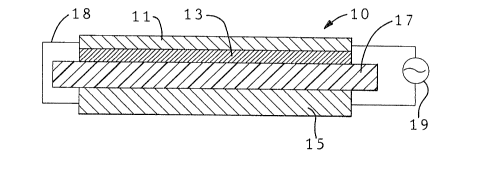
FIGURE 1 is a view in longitudinal section of a self-
regulating heater useful in various embodiments of the present
I 10 invention;
FIGURE 2 is a view in longitudinal section of another
self-regulating heater useful in various embodiments of the
present invention;
7a
`;`
~ 3 ~
FIGURE 3 is a view in perspective of a surface mount
connector and heater assemhly arranged in accordance with
the principles o~ the present invention;
FIGURE 4 is a view in transverse section of a surface
mount connector and heater assembly , such as illustrated
in Figure 3, disposed on a circuit board in accordance
with the principles of the present invention;
FIGURE 5 is a view in transverse section of an
alternative embodiment of the surface mount connector and
heater assembly of the present invention; and
FIGURE 6 is a view in transversP ssction of still
another surface mount connector and heater assembly of the
present invention.
Referring specifically to Figure 1 of the
accompanying drawings, there is illustrated a
self-regulating heater 10 for use in soldering terminals
of a surface mount connector to circuit board contact
pads, or the like. The heater includes an elongated
- rectangular substrate 11 of copper or other material
having a high electrical conductivity (i.e., low
resistivity) and negligible magnetic permeability (i.e., a
permeability of, or close to, one)O The substrate
material must also be a good thermal conductor. Substrate
11 typically, although not necessarily, has a length much
greater than its width which, in turn, i5 much greater
; than its thickness. As an example of these relative
14323 CA -8
3 3
dimensions, the substrate length may be threP inches, its
width may range from one-tenth to one-half inch, and its
thickness may range from 0.005 t~ 0.010 inch. It should
be noted that the rectangular substrate configuration
illustrated in Figure 1 is merely an exemplary
configuration and that substantially any configuration,
consistent with the principles described herein, may be
employed.
A thermally-conductive skin layer 13 of magnetic
material is deposited or otherwise disposed over one
surface of substrate 11. In the illustrated embodiment
surface layer 13 is disposed over the entirety of that
surface but may be disposed only on selected surface
portions. A typical material for layer 13 is nickel-iron
alloy, such as Alloy 42 (forty-two percent nickel,
fifty-eight percent iron), or Alloy 42-6 (forty-two
percent nickel, six percent chromium, fifty-two percent
iron~; however, layer 13 may be any metal or alloy having
the characteristics described herein. Depending upon the
particular material, magnetic permeabilities for layer 13
range from fifty to more than one thousand, as compared to
a permeability of one for copper; typical electrical
resistivities for layer 13 range from twenty to ninety
micro-ohms per centimeter as compared to 1.72 for copper.
The thickness of surface layer 13 is typically one skin
depth. In this regard, substrate 11 and layer 13, when
14323 CA -9-
~ 3 ~
energized by passing a constant amplitude alternating
current therethrough, function as a self-regulating
heater. Specifically, for temperatures below the Curie
temperature of the material of surface layer 13, slightly
more than sixty-three percent of the constant amplitude
current flowing through the heater is concentrated in one
skin depth from the heater surface. The skin depth is
proportional to the square root of the material
resistivity, and is inversely proportional to the square
root of the product of the magnetic permeability of
surface layer 13 and the frequency of the alternating
current passing through the heater. At temperatures equal
to or above the Curie temperature of the surface layer 13
material, the magnetic permeability of that material drops
to approximately that of the substrate material (i.e., a
permeability of one, for copper), thereby producing a
dramatic increase in the surface depth. Consequently,
much more of the constant amplitude current is distrib~ted
in the lower resistivity substrate 11 than in higher
resistivity surface layer 13, with the result that
considerably less heat is dissipated. Importantly, if
selected locations of ths heater body are in contact with
thermal energy absorptive loads (e.g., heat sinks), then
the temperature at those locations of the heater body does
not rise as readily as it does at the non-load locations.
It is possible, therefore, for the constant amplituds
14323 CA -10-
~3~ ~38
current to be concentrated in surface layer 13 to a
greater extent at the load locations (where the
temperature is below the Curie temperature for surface
layer 13) than at the non-load locations (where the
temperature is equal to the Curie temperature of surface
layer material 13). Curie temperatures for materials can
range from 50C to 1,000C; typical materials employed for
surface layer 13 have Curie temperatures in the range of
200C to 500C, depending on the solder or fusing material
employed.
In order to actuate the heater, a tooling assembly is
employed and comprises an electrically-conductive bus bar
layer 15 and a superposed layer 17 of electrically
insulative material. Bus bar layer 15 is typically copper
and has dimensions similar to those of substrate 11.
Insulative layer 17 is typically Kapton and is slightly
larger in length and width than the corresponding
; substrate dimensions; the thickness of layer 17 is of the
same order of magnitud as that of the substrate. The
tooling assembly may be secured flush against heater body
assembly 10, as illustrated in Figure 1, with the exposed
surface of the insulative layer 17 abutting surface layer
13. Under such circumstances the heater body and tooling
assembly may be held together permanently by adhesive
disposed between layers, or any other technique that joins
the tooling to the heater body in flush abutting relation.
14323 CA
~ 3 ~
Alternatively, the tooling assembly may be selectively
movable into and out of flush contact with the heater
body.
A source 19 of constant amplitude alternating current
is connected across the heater body assembly (at substrate
11) and the tooling assembly (at bus bar layer 15) at one
end of the heater assembly. Source 19 may be any suitable
const~nt amplitude alternatir~g current supply such as, for
example, the source disclosed in U.S. Patent No. 4,626,767
(Clappier et al) and provides a constant amplitude
alternating signal, typically in the radio fre~uency
range. Most commonly, the frequency of the actuating
signal is 13.56 MHz. The constant amplitude of the signal
is selected to provide the desired heating level. An
impedance matching circuit is typically provided to match
the impedance of the heater-tooling combination to the
source impedance~ At the end of the heater body located
longitudinally remote from the connection to source 19
there is a wire 18 or other short circuit interconnecting
substrate 11 and bus bar 15. Current flow through the
combination, there~ore, at any instant o~ time, is in
longitudinally opposite directions in heater 10 (i.e., in
substrate 11 and layer 13), and bus bar 15. A resulting
electric field is established between heater 10 and bus
bar 15 across insulation layer 17, thereby concentrating
the current flowing through the heater assembly in the
14323 CA -12-
13~ ~ 3~
high resistance surface layer 13 rather than in khe low
resistance outer surface of substrate 11. The current
flowing through bus bar layer 15 is concentrated at the
surface facing the heater assembly 10. Since the current
amplitude is maintained constant, it is desirable, for
optimal heating, to concentrate the current in the high
resistance surface layer 13 of heater assembly 10 rather
than in the low resistance substrate 11. That is, the
resistive heating, with the current maintained constant,
is greater when the current path has greater resistance.
The electric field developed by the oppositely-directed
current flowing in the heater assembly and bus bar 15
assures that the current in the heater assembly is
concentra~ed in the high resistance surface region of the
heater assembly facing the bus bar.
As described below, a plurality of spaced terminals
(not visible in Figure 1) extend from heater body 10. The
terminals are preferably formed integrally with the heater
body and are thermally conductive so as to transfer
thermal energy from the heater 10~ In the embodiment
illustrated in Figure 1 the terminals extend into the
plane of the drawing and are spaced along the horizontal
dimension of the drawing. The thermal energy resulting
from the resistive heating at heater 10 is conducted by
the various terminals to connection sites in order to melt
solder that is deposited in pre-determined amounts at
14323 CA -13-
1 3 ~
those sites, typically on the contact pads of a circuit
board. A typical solder is 63 percent tin with the
balance being lead, having a melting point of 183 C.
The nature of heater assembly 10 is such that the
resistive heating is produced only where it is needed to
effect the soldering operations. More specifically,
current through heater assembly 10 flows longitudinally
and thereby alternately encounters regions from which the
terminals pxoject and regions corresponding to spaces
between the terminals. Thermal energy developed in
regions proximate the terminals is conducted to respective
connection sites by the terminals, thereby preventing the
temperature at those regions ~rom building up quickly. On
the other hand, in the regions corresponding to spaces
between terminals, the temperature increases rapidly until
it reaches the Curie temperature of the material of the
surface layer 13, whereupon the effective skin depth is
increased dramatically in those regions. This results in
more current flowing through the low resistance substrate
material in these regions and, as a consequence, less
thermal energy is produced therein. The regions proximate
the terminals continue to develop high amounts of thermal
energy that is conducted to respectiva connection sites.
Overheating of the connection sites is prevented by the
same mechanism; that is, once the temperature at the
connection site reaches a certain level, thermal
14323 CA -14-
13~38
conduction from the heater to the site ceases, thereby
remo~ing the heat sink effect of the connection site. The
thermal energy developed by the current flowing in high
resistance layer 13 then guickly increases the temperature
proximate the terminals until the Curie temperature of the
material is reached. At this point the effective skin
depth along the entira length of the heater assembly is
increased so that more of the constant amplitude current
flows through the low resistance substrate 11 and
significantly less energy is produced by resistive
heating. After current is removed from the heater
assembly, the assembly begins to cool and the solder is
permitted to solidify. The cooling proceeds quickly
because the relatively low mass of the heater does not
retain its heat for long periods of time.
An alternative self-regulating heater 20 is
illustrated in Figure 2 of the accompanying drawings and
develops its heater current by means o~ electromagnetic
induction rather than by direct conduction. The heater 20
takes the form of an elongated (i.e., in the horizontal
dimension of the drawing) substrate 21 o~ copper, or the
like, the opposite surfaces of which are coated with
respective surface layers 23, 25 o~ magnetic alloy or
similar metal. Heater 20 also has at least one row of
terminals secured thereto ~not visible in Figure 2 but
extending into the plane of the drawing) in the manner
14323 CA -15-
.
.:
~ 3 ~
described above in relation to heater 10. The terminals
are in thermally-conductive relation with the heater. A
tooling member for applying current to heater 20 comprises
a primary conductor 27 formecl as an elongated strip of
copper, or the like, bent in a U-shaped configuration.
The inside surface of conductor 27 has a strip 29 of
electrically-insulative material disposed thereon and
extending over most of the length of the conductor. In
use, heater 20 is disposed between the legs of the
U-shaped primary conductor 27 and may either be spaced (as
shown) by an air gap from the insulative strip 29, or may
contact the insulative strip in flush abutting relation at
each surface layer 23, 25. In either case, the heater 20
is typically held in place within primary conductor 27 by
appropriate tooling attachments (not shown). For example,
any suitable Plectrically-insulative bracket secured to
~trip 27 may be adapted to support heater 20 within the
primary conductor confin~s.
In operation a source 19 of constant amplitude
alternating current is connected across the distal ends of
the U-shaped primary conductor 27. That conductor
functions as a primary winding of a transformer to induce
eddy currents in the heater strip 20 which serves as the
secondary winding. The induced eddy currents, as is
well-known, tend to flow in planes perpendicular to the
magnetic flux developed by the primary current. The flux
14323 CA -16-
~ 3~38
produced by the alternating primary current in conductor
27 is directed perpendicularly to the surfaces of heater
20; therefore, the induced eddy currents flow in planes
parallel to the heater surface. The eddy currents are
subject to the skin effect phLenomenon and, therefore,
concentrate in the high-resistance surface layers 23, 25
for temperatures below the Curie temperature of the skin
layer material. The amplitucle of the primary current is
selected such that the resistive heating resulting from
the eddy currents in the surface layers is sufficient to
heat the terminals projecting from the heater 20 to the
temperature required to melt solder deposited at the
connection sites. After a soldering operation the
terminals may be severed from ~he heater assembly in the
manner described below.
Currents may also be electromagnetically induced in
heater assembly 20 by means of a primary circuit
comprising a number of turns of wire wrapped about the
heater with insulation or an air gap interposed between
the heater and the turns of wire. Electromagnetic
induction of the heating current may also be effected by
the transformer configuration de~cribed in U.S. Patent No.
4,745,264 (Carter).
It is to be understood that the self-regulating
heater embodiments 10, 20 described above are only
14323 CA -17-
~3~3~
examples of heaters that may be employed in connection
with the present invention.
Referring to Figures 3 and 4 of the accompanying
drawings, a surface mount connector 30 includes a housing
in which a plurality of terminal-receiving passages 31 are
defined. Each passage 31 is adapted to receive a
respective terminal 33 through the underside of the
housing in the manner described, for example, in U.S.
Patent No. 4,693,528 (Asick et al) or 4,645,287 (Olsson),
the terminals 33 being of either the pin or socket type.
In accordance with the present invention the terminals
are located at the distal ends of respective projections
from one or more self-regulating heaters 35 of the type
described above. The projections are typically copper and
formed integrally with heaters 35. The proximal ends of
the projections are joined to the heaters at transverse
score lines 37 of reduced thickness to facilitate severing
of the projections from the heaters after a soldering
operation. Located intermediate terminals 33 and score
lines 37 on each projection there is a solder tail portion
39 adapted to be placed in abutting relation against a
respective contact pad 41 on a circuit board 40. The
spacing between the terminal projections along the length
of heaters 35 is chosen to assure that the solder tails 39
do, in fact, overlie respective contact pads 41.
14323 CA -18-
An assembly comprising surface mount connector 30 and
heater 35 with its projecting terminals may be assembled
and stored until the connector is to be soldered to a
circuit board 40. At that time the assembly is positioned
on the circuit board with solder tails 39 resting on
respective contact pads 41 to define respective connection
sites. Solder or other fusible electrically-conductive
material is typically pre-deposited in measured amounts on
each contact pad 41, but may be pre-deposited on the
solder tails or delivered to the connection site during
the soldering procedure. Tooling 43, which may be
permanently secured to the heater 35 or selectively
brought into contact therewith, is utilized as described
above to permit actuation of the heater via a source 19.
The heater operates in the manner described above to
conduct thermal energy to each solder tail 39 and contact
pad 41 simultaneously to melt the solder. Once the solder
has melted, the current is removed from the heater to
permit the solder to harden, after which the heaters are
removed from the terminals 33 along score lines 37.
For some applications the terminals are only
partially inserted into respective passages 31 in tha
connector housing prior to soldering; once the solder
connections have been made the terminals may be fully
inserted into the passages, usually in a snap-fit
engagement. ~lternatively, the terminals may be fully
14323 CA -19-
:~3~3~
67789~274
inserted into the passa~es prior to the soldering operation.
As noted above r terminals 33 may be either pins or
sockets. For certain types of socket terminals it is desirable to
utili~e two juxtaposed heater elements with their prOJecting
terminals interdigitated. More particularly, and referriny to
Figure 5 of the accompanying drawillgs, a terminal carrier strip is
formed from two self-regulating heater se~tions 50, 51 positioned
on opposite sides of a strip 56 of insulation material sueh as
Kapton. Heater section 50 includes an elongated generally
rectangular substrate 52 of copper or other material having a high
electrical conductivity and negligible magnetic permeability. A
layer 53 of ~agnetic material is deposited or otherwise disposed
over one surface of substrate 52. A plurality of electrical
terminals 33 extend from one longitudinal edge of substrate 52 in
spaced relation. As in the previously discussed embodiments, the
terminals 33 are adapted to be received in appropriate terminal-
receiving passages in a connector housing. The second heater
section 51 is substantially identical to heater section 50 and
includes substrate 54 with magnetic layer 55 disposed on one
surfa~e facing magnetic layer 53 o~ heater section 50. The
insulation
2Q
`'``` ' `i
.,~,
3 ~
layer 56 is disposed between the two magnetic layers 53
and 55. A plurality of electrical terminals 33 also
extend from substrate 54 in spaced relation. The edge of
substrate 52 from which terminals 33 extend is aligned
with the edge of substrate 54 from which its terminals
extend, thereby positioning the two sets of terminals
along the same edge of the overall carrier strip. The
spacing between the terminals extending from substrate 52
is substantially the same as the spacing between the
terminals extending from substrate 54 and is such the two
sets of terminals are interdigitated. When performing a
solder operation, a source of constant amplitude
alternating current is typically connected between heater
sections 50 and 51 at one longitudinal end of the
assembly; a short circuit is typically connected between
the two heater sections at the opposite end of the
assembly. An electric field developed between the two
heater sections across the insulation layer 56
concentrates the current flow in the two mutually-facing
surfaces of the heater sections where the magnetic layers
are disposed.
The embodiment illustrated in Figure 6 includes an
edge-type surface mount connector 60 adapted to be
connected to arrays of contact pads 61, 63 disposed on
opposite surfaces of a circuit board 65. One set of
terminals 67 for connector 60 is secured to
14323 CA -21-
- !
131~3~
self-regulating heater 68 and is arranged to have the
solder tails for those te~ninal contact respective contact
pads 61; a second set of terminals 69 is secured to
self-regulating heater 70 ancl is arranged to have the
solder tails for those terminals simultaneously contact
respective contact pads 63. ~y means of appropriate
tooling the heaters 68 and 70 may be actuated with
constant amplitude alternating current to effect the
solder connections at the various connection sites in the
manner described above.
As described above, the connection sites are most
efficiently heated to the soldering temperature by
automatic self-regulating heaters. It is to be
understood, however, that the readily severable terminals
may also be used in conjunction with other typ~s of
heaters, including nichrome wire and hot bar heaters.
For the embodiments illustrated in Figures 3, 4 and
5, two separate heater assemblies are described as being
positioned on opposite sides of a surfac~ mount connector
being joined to a board. It will be appreciated by those
skilled in the art that a single heater assembly
configured lengthwise in the shape of a U can be similarly
employed such that the two legs of the U correspond to the
individual heaters described above.
Although solder is the preferred fusible electrically
conductive material for most applications of the present
14323 CA -22-
~31~38
invention, other such materials may be employed. For
example, several conductive adhesives and pastes are
commercially available and are fabricated as suspensions
of metal powder in a thermosetting plastic. The metal
powders employed are typically gold, silv~r, copper,
aluminum etc., while the adhesive plastic is generally
epoxy-type resin.
From the foregoing description it will be appreciated
that the present invention makes available a novel method
and apparatus for simultaneously joining plural terminals
of a surface mount connector to respective contact pads on
a printed circuit board, or the like, wherein only the two
components to be joined at each connection site require
alignment and wherein thermal energy is delivered only to
the connection sites and not over a large area
encompassing all of those sites.
Having described preferred embodiments of a new and
improved method and apparatus for connecting a surface
mount connector to a circuit board, or the like, it is
believed that other modifications, variations and changes
will be suggested to thosa skilled in the art in view of
the teachings set forth herein. It is therefore to be
understood that all such variations, modifications and
; changes are believed to fall within the scope of the
present invention as defined by the appended claims.
14323 CA -23-