Note: Descriptions are shown in the official language in which they were submitted.
1310376
-1- RCA 83, 957A
CURRENT GAIN COMPE~7~;ATION A~PLIFIE~
The invention relates to an amplifier arrangement
that combines an input siynal with a reference signal to
produce an output signal that is level shifted relative to
that of the input signal. In particular, the invention
relates to a level shifter used in an input stage of a power
supply regulator of a television apparatus.
In a power supply arrangement o~, ~or example, a
television receiver, a voltage representative of a DC,
regulated supply voltage B+ is coupled to, for example, an
inverting input terminal of a B+ voltage regulator. A
reference voltage is coupled to, for example, a noninverting
input terminal of the regulator. The feed-back voltage that
is representative, for example, of regulated supply voltage
B+ is compared, in the input stagP, with the reference
voltage to generate an output voltage that is coupled to a
controllable arrangement. The controllable arrangement
regulates voltage B+ at a level that is determined by the
reference voltage. Voltage B+ may be used, for example, to
energize a deflection circuit output stage for a cathode ray
tube (CRT).
In one prior art circuit, a voltage representative
of, for example, a level of the beam current in the CRT is
summed with the reference voltage, such that the sum of
both, instead of the reference voltage alone, is applied to
the noninverting input terminal of the input stage, a
variation of the beam current representative voltage varies
voltage B~ so as to maintain constant the raster width in
the C~T when the beam current changes.
The summation of the constant reference voltage and
the variable beam current representative voltage is done,
in such prior art circuit, by coupling the beam current
representative voltage via a zener diode to the
noninverting input terminal. The zener diode develops
between its anode and cathode electrodes the referenc~
voltage. Thus, the reference voltage that level shifts the
A :~-
-2- 1 3 1 0 37 ~CA ~3,9~7
beam current representative voltage is series coupled with
the beam current representative voltage.
A disadvantage of such zener diode level shifting
is that a change in the zener voltage due to temperature,
aging or an inherent noise in the zener diode, causes the
level to change.
It may be desirable to sum the beam current
repres~ntative voltage with a reference voltage to generate
a sum voltage that ls applied to the noninverting input
terminal of the input stage without using such zener diode.
In an embodiment of the invention, the reference
voltage is produced by a voltage source of, for example,
the well known bandgap type. The beam current
representative voltage is summed with, or level shifted by,
the reference voltage that is produced by the bandgap type
source. Advantageously, the bandgap type source is less
susceptible than the zener diode to temperature changes,
component aging or noise.
In a circuit embodying an aspect of the
invention, an input signal, such as a beam current
representative voltage, is coupled in series with an
emitter electrode of a first transistor that operates as a
common base amplifier. A second transistor, operating as a
current source, and having its collector coupled to the
collector of the first transistor, supplies the collector
current of the first transistor. A current mirror
arrangement, that includes the first transistor, causes the
collector current in the first transistox to be equal to
that supplied by the collector current of the second
transistor, when the input signal is at a predetermined
magnitude such as zero. A first voltage, such as produced
by a bandgap type source, is coupled via a resistor to a
junction terminal between the collectors of the first and
second transistors. The collector currents of the first
and second transistors produce a difference current that
develops a voltage across the resistor that is summed with
the first voltage to produce a second signal that is
-3~ t310376
RCA 83,9~7
developed at the junction terminal. The second signal is
at a magnitude that is determined by the first voltage and
not by the collector currents in any of the first and
second transistors, ~hen the magnitude of the input signal
is predetermined such as zero. When the magnitude of the
input signal is different from the predetermined magnitude,
the second signal is different from the first voltage by an
amount that is proportional to the magnitude of the input
signal.
In accordance with an aspect of the invention, a
pQWer supply includes a level shifter level that shifts an
input voltage used for controlling an output supply voltage
of the power supply. A controllable conductive element is
coupled to the input supply voltage for generating, from
the input supply voltage, the output supply voltage. The
power supply includes a comparator, coupled to the
conductive element, for varying, in accordance with an
output signal of the comparator, the conduction of the
conductive element to control the output supply voltage. A
current mirror arrangement that in~ludes a ~ransistor i~
responsive to a current in a first circuit branch for
generating in a first main current conducting electrode of
the transistor a current that is the current mirror cf the
current in the first circuit branch. The first main curren~
conducting electrode is coupled at a junction terminal to a
second circuit branch for conducting at least a portion of
a current in the second circuit branch. A source of the
input voltage is coupled to the transistor for varying the
current in the first main current conducting electrode to
produce a difference related current that varies in
accordance with the input voltage. The difference current
is related to a difference between the current in the first
main current conducting electrode and the current in the
second circuit branch. A first resistance is coupled to
the junction terminal for conducting the difference related
current to develop a voltage across the resistance that
varies in accordance with the input voltage. A source o~
temperature compensated first voltage is coupled via the
~4~ 1 31 037~
RCA ~3,9~7
resistance to the junction terminal such that the voltage
across the resistance is combined with the first voltage
for developing a temperature compensated second voltage at
the junction terminal. The second voltage varies in
accordance with the input voltage. The second voltage is
level shifted in accordance with the first voltage. The
temperature compensated, level shifted, second voltage is
coupled to an input of the comparator for varying the
output signal of the comparator to control the output
supply voltage~
In the Drawing:
FIGURE 1 illustrates a simplified schematic
diagram of a power supply regulator circuit that includes a
level shifter, embodying an aspect of the invention;
FIGURE 2 illustrates a detailed schematic diagram
of the level shifter of FIGURE 1; and
FIGURES 3, 4, 5 and 6 illustrate level shifters
embodying different aspects of the invention, respectively.
FIGURE 1 illustrates a simplified schematic
diagram of a power supply of a television receiver, not
shown in the FI~URES, that includes a regulator 100 that is
an integrated circuit that regulates a supply voltage B+.
Voltage B+ may be used, for example, to energize a
horizontal deflection circuit or output stage 99 of the
television receiver.
A voltage V-~, representative of voltage B+, is
obtained from output stage 99. Voltage V+ is coupled to a
voltage divider 605 that includes series coupled resistors
601, 604 and 602. Resistor 604 includes a wiper k for
developing at wiper k a voltage that is representative of,
for example, voltage B+. The voltage at wiper k, that is
adjustable by varying the position of wiper k, is coupled
to an inverting input terminal 608 of an error amplifier
610 via a resistor 607.
A small voltage that is proportional to the beam
current in the CRT of the receiver is coupled from a
1 3 1 0376 RCA ~3,957
-tertiary wlnding of transformer T to a terminal 611 to form
a voltage VNINI that is indicative of the beam current.
Voltage VNINI that varies when a variation of
the beam current occurs, is coupled via a level shifter
600, embodying an aspect of the invention, to a
noninverting input terminal 609 of error amplifier 610 to
produce an input voltage VNIN. Level shifter 600
establishes a fixed offset voltage between terminals 611
and 609 that is determined by a voltage VBG. Voltage VBG
is generated in a bandgap type voltage source 699. Bandgap
type voltage source 699 advantageously maintains voltage
VBG constant such that voltage VBG is affected
significantly less by component aging or tolerance than
would have occurred had a zener diode been used. As
explained later on the feed back arrangement of regulator
100 causes voltage B~ to be such that voltage VIN becomes
equal to voltage VNIN.
An integrating filter 612 is coupled between
inverting input terminal 608 and an output terminal 618 of
amplifier 610 to pr~vide the loop filter of reaulator 100.
A filtered error voltage V0, developed at terminal 618 is
coupled to a first input terminal of an adder 613. A
horizontal rate sawtooth generator 98 develops a horiæontal
rate signal, having an upramping portion, which is added to
error voltage V0 in adder 613. The sum signal that is also
upramping, is applied to an inverting input terminal ~614~
of a comparator 615 functioning as a pulse width modulator.
When, during its upramping portion, the output of
adder 613 becomes more positive than a constant DC voltage
VREF, that is coupled to a noninverting input terminal of
comparator 615, a negative going transition at an output
terminal 615a of comparator 615 is coupled via a buffer
amplifier 616 to a control terminal 617a of a switch 617b
of a switch mode power supply output stage 617 to turn on
switch 617b of output stage 617.
An input terminal 617c of output stage 617 is
coupled to unregulated voltage VuR. Regulated voltage B+
-6-t 3 1 ~37 ~
RCA ~3,9~7
is developed at an output terminal 617d of output stage
617.
The duration, during each horizontal period, H,
in which switch 617b conducts is determined by the level of
error voltage V0 of error amplifier 610. Thus, regulatèd
voltage B+ is determined by voltage VNI~. As indicated
before, voltage VNIN is produced by level shifter 600,
embodying an aspect of the invention, that is described now
in detail.
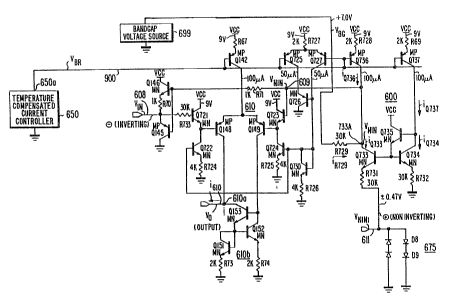
FIGURE 2 illustrates a schematic diagram of level
shifter 600 of FIGUP~ 1 and of error amplifier 610.
Similar numbers in FIGURES 1 and 2 represent similar items
or functions. Level shifter 600 of FIGURE 2 is temperature
compensated over a wide range of ambient operating
temperatures, such as between 0C and 70C, to produce
voltage VNIN that is suhstantially unaffected by a change
in the temperature within such range.
A temperature compensated current control
arrangement 650 generates a control voltage VBR on a rail
signal line 900. Rail signal line 900 is coupled to the
base electrode of each of transistors Q142, Q725, Q727,
Q736 and Q737. The emitter electrodes of the
above-mentioned transistors are coupled through
corresponding resistors to a fixed DC voltage Vcc. Current
control arrangement 650 controls voltage VBR in such a way
that the collector current in each of the above-mentioned
transistor stays substantially constant when the
temperature changes. An example of an arrangement that is
similar to current control arrangement 650 is described in
detail in U.S. Patent No. 3,886,435, in the name of S. A.
Steckler, entitled VBE VOLTAGE SOURCE TEMPERATURE
COMPENSATION NETWORK.
Level shifter 600 includes transistors Q736 and
Q737. The emitter currents in transistors Q736 and Q737
are controlled by resistors R728 and R69, respectively,
having the same value, so as to cause the respective
collector currents of transistors Q736 and Q737, that are
temperature compensated, to be equal. The collector of
--7--
1 31 0376 ~CA z3,957
transistor Q737 is coupled to a current mirror arrangement
that includes transistors Q733, Q734 and Q735. The
collector of transistor Q737 is coupled to the collector of
transistor Q734. The emitter of transistor Q735 is coupled
to each of the bases of transistors Q733 and Q734.
Transistor Q735 provides the base current drive to each of
transistors Q733 and Q734. The emitter of transistor Q734
is coupled to ground via a resistor R732. The P-N junctiun
of transistor Q734 be~ween the base and emitter electrodes
of transistor Q734, provides temperature compensation that
compensates for a temperature related variation of the
base-emitter voltage of transistor Q733. The emitter of
transistor Q733 is coupled through resistor R731 to
terminal 611, where voltage VNINI of FIGURE 1 is developed~.
The value of resistor R731 is equal to that of resistor
R732- Voltage VNINI is prevented from exceeding
predetermined limits in either polarity by a diode network
675. The collector of transistor Q733 is coupled to the
collector of transistor Q736 at a junction terminal 733A.
Assume th2t volta~e VNINI is zero. In this cas~,
the current mirror arrangement of transistors Q733, Q734-
and Q735, produces a collector current iQ733 in transistor
Q733 that is equal to the collectox current iQ734 in
transistor Q734 because the base current of transistor Q735
is negligible. As explained before, when voltage VNINI is
zero, collector current iQ736 in transistor Q736 is equal
to collector current iQ737 in transistor Q737 over a wide.
temperature range. Also, when voltage VNINI is zero, each
of collector current iQ733 that is the current mirror of.
curren~ iQ734 is equal to current iQ737 over such wide
temperature range. It follows that current iQ733 is also
e~ual to current iQ736~
Bandgap type voltage source 699 supplies
temperature compensated reference voltage VBG that is
coupled via a resistor R729 to terminal 733A. Because, as
described before, when voltage VNINI is zero, current i
is supplied entirely by current iQ736~ and because the
impedance at terminal 733A, that is contributed by the
1 3 1 Q376 RCA 83,957
collectors of tr~nsistors Q733 and Q736 is high, a current
iR729 in resistor R729 is zero; therefore, voltage VNIN at
tenminal 733A is equal to voltage vB&. Thus, in accordance
with an aspect of the inventio~, when voltage VNINI is
zero, voltage VNIN is level shifted by an amount that is
equal to voltage VBG~
When voltage VNINI at terminal 611 is different
from zero, currents iQ736 and iQ737 will not be equal. The
difference current between currents iQ733 and iQ736 will
cause a voltage to develop across resistor R729 that, i~
turn, will cause a corresponding change in voltage VNIN at
terminal 733A. Because transistor Q733 is coupled,
relative to voltage ~ INI~ as a common base amplifier, and
because resistors R731 and R72g are, illustratively,
equal, the gain, or the ratio between voltage VNIN and
voltage VNINI, is one, resulting in an amplifier having a
unity gain.
In carrying out another aspect of the invention,
voltage VNIN, that is level shifted relative to voltage
VNI~I by an amount that is equal to voltage VBG, follows
v~riations of voltage VNINI that occur in a range betwee~
positive and negative values.
Voltage VB& i5 temperature compensated and has a
tolerance range that is narrow relative to, for example, a
zener diode. Furthermore, component aging affects voltage
VBG substantially less than it affects, for example, the
breakdown voltage of a zener diode. Moreover, the level
shifting caused by level shifter 600 is, advantageously,
less susceptible to temperature, aging and noise when
compared with that produced by a corresponding level
shifter in the prior art that utilizes a zener diode
interposed between a beam current input terminal and a
noninverting input terminal of a differential amplifier to
perform such level shifting.
Should a temperature change cause a corresponding
change in current iQ736~ for example, that, as ind~cated
before, would be relatively small, transistors Q737, Q733,
Q734 and Q735 will cause a proportional change in current
1 31 0376 RCA 83,957
iQ733 to occur that will prevent even such small change in
temperature from affecting the difference current between
currents iQ736 and iQ733. Therefore, when voltage VNINI is
zero, voltage VNIN is, advantageously, not affected by
collector currents iQ736 and iQ737~
detenmined by voltage VBG that is temperature compensated.
It should be understood that temperature
compensation may be adequate even when voltage VNINI is
significantly different from zero. If temperature
compensation, in this case, is inadeguate, a further
improvement in temperature compensation may be obtained by
coupling the terminal of, for example, resistor R732, that,
in FIGURE 2 is grounded, to a voltage that is different
from zero and that is related to, for example, voltage
VNINI
Advantageously, voltage VBG, as explained before,
is maintained at tight tolerances, is temperature
compensated and is substantially unaffected by components
aging. Therefore, advantageously, no factory temperature
burn-in process is required prior-to the installment of
regulator 100 of FIGURE 1 in the television receiver.
Furthermore, voltage divider 605 that includes resistors
601, 604 and 602 is required to compensate, advantageously,
only for a narrower tolerance range than in prior art
circuits in which a zener diode is used for performing the
level shifting function of level shifter 600 of FI~URE 2.
Voltage VIN is coupled to the base of a
transistor Q721 The clamping operation of a pair of
trans~stors Q145 and Q146 prevents voltage VIN from being
above voltage VBG or from being below voltage VB~ by more
than a predetermined magnitude. Voltage VIN is coupled to
inverting input terminal 60~ and voltage VNIN is coupled to
noninverting input terminal 609 of error amplifier 610.
Amplifier 610 includes a current source formed by a
transistor Q142 that provides the combined emitter currents
of a transistor Q148 and of a transistor Q149, coupled as a
differential amplifier. The bases of transistors Q148 and
Q149 are coupled to the emitters of transistors Q721 and
1310376
-10- RC~ 83,957A
Q723 respectively. Transistors Q721 and Q723 operate as
emitter followers to couple voltages VIN and VNIN to the
base of transistors Q148 and Q149, respectively.
A transistor Q722 has a collector electrode that
is coupled between the base and emitter electrodes of
transistors Q148 and Q721, respectively. A collector
current ic of transistor Q722 is equal to a sum of a base
current ibQ148 of transistor Q148 and of an emitter current
ie f transistor Q721 for supplying both the base current
and the emitter current, respectively. The base electrode
of transistor Q722 is coupled to the collector of
transistor Q730 for varying collector current ic in a
manner that compensates for current gain changes in
transistor Q148, as described later on. The collector
electrode of transistor Q730 is coupled as a diode, that
forms with transistor Q722 a current mirror arrangement.
Transistor Q727, having a base electrode that is coupled to
voltage VBR generates a temperature compensated collector
current that is unaffected hy current gain variation of
transistor Q727, as indicated before. A current iQ727 is
coupled also to the collector terminal of transistor Q730
such that collector current iQ727 in transistor ~727
provides a first portion of the collector current of
transistor Q730.
In accordance with a feature of the invention, the
first portion is independent of current gain variations or
deviations of transistor Q727. A second portion of the
collector current of transistor Q730 is provided by a base
current ibQ726 f a transistor Q726 that is summed with
current iQ727 to form a sum current iSum that is coupled to
the collector terminal of transistor Q730. The second
portion that provides current gain compensation is
dependent on the current gain of transistor Q726.
The current gain of transistor Q726 follows or
tracks in the same sense changes or variations of the
A
1 31 0376
- lOA- RCA 83,957A
current gain of transistor Q148, occurring due to, for
example, temperature or tolerances. This is accomplished,
for example, by constructing the two P-N-P transistors r~Jith
the same geometry using a similar process and by
5 maintaining the operating temperature of the two
transistors the same.
In steady state operation of the differential
am~lifier, the emitter current in each of transistors Q148
and Q726 is substantially the same. The nominal emitter
currents in transistors Q148 and Q726 are, each, for
example, 50 microamperes, as controlled via transistors
Q142 and Q725, respectively. As explained before, the
collector currents in transistors Q142 and Q725 that are
controlled by voltage VBR are temperature compensated. A
deviation in base current ibQ148 will be accompanied with
the same sense deviation in the base current ibQ726 of
transistor Q726 and, therefore, also in the collector
current of transistor Q730. Because of current mirror
operation formed by the arrangement that includes
transistors Q722 and Q730, a change in base current ibQ726
of transistor Q726 will cause substantially the same sense
change in the collector current of each of transistors Q730
and Q722.
Therefore, in accordance with another feature of
the invention, the change in base current ibQ148 of
transistor Q148 will be, advantageously, compensated by the
corresponding equal change of the collector current of
transistor Q722. The change in the collector current of
transistor Q722 is in the same sense so as to prevent the
emitter current of transistor Q721 from changing or
deviating from its nominal value when base current ibQ148
of transistor Q148 changes. The emitter current of
transistor Q721 will be determined by collector current
iQ727. Current iQ727 is independent of current gain
variations, as explained before.
t 3 1 0376
-lOB- RCA 83,957A
In accordance with an aspect of the invention,
transistor Q722 that is included in the current mirror
arrangement generates both a first current portion and a
second current portion. The first current portion
maintains the emitter current of transistor Q721,
advantageously, independent of the current gain of
transistor Q148 and the second current portion supplies the
base current of transistor Q148. It should be understood
that since transistors Q722, Q724 and Q730 are of the N-P-N
type, having a high current gain, their base currents may
be ignored in this analysis.
Similarly, a change in the base current of
transistor Q149 will be compensated by a corresponding
change in a collector current of a transistor Q724. The
collector current of transistor Q724 is controlled in the
same manner as that of transistor Q722.
The emitter currents of each of transistors Q721
and Q723 are, each, for example, not significantly larger
than each of the base currents of transistors Q148 and
Q149, respectively. The emitter currents in transistors
Q721 and Q723 are, advantageously, maintained substantially
unaffected by variation or change of the current gain of
transistors Q148 and Q149. As explained before, such
changes and variations may occur due to temperature or
tolerances. Therefore, advantageously, the offset voltage
of amplifier 610 is less affected by current gain changes
of transistors Q148 and Q149. It follows that voltage
regulation tolerances in the power supply are improved.
Additionally, the current gain compensation will,
advantageously, prevent even an excessive current ibQ148,
for example, from cutting off transistor Q721.
In accordance with another aspect of the
invention, deviations of the current gain characteristic of
transistors Q148 and Q149 are sensed in transistor Q726
that is coupled outside the signal path in the differential
1 31 0376
-lOC- RCA 83,957
amplifier. Transistor Q726 is also coupled outside the
current paths in each of transistGrs Q148 and Q149 that
form the differential amplifier.
A current mirror arrangement 610 that is coupled
to the collectors of transistors Q14~ and Q149 that forms
the differential amplifier causes a current i610/ coupled
to integrating filter 612 of FIGURE 1, to be equal to the
difference between the collector currents in transistors
Q148 and Q153. Consequently, current i6lo that is coupled
to filter 612 of FIGURE 1, is proportional to the
difference between voltages VIN and VNIN- The
proportionality factor is determined by the gain of error
amplifier 610 that is determined by transistors Q14~ and
Q149.
A current mirror arrangement 610b that is coupled
to the collectors of transistors Q148 and Q149 causes a
current i610/ coupled to integrating filter 612 of FIGURE
1, to be equal to the difference between the collector
currents in transistors Q143 and Q153. Consequently,
current i610 that is coupled to filter 612 of FIGURE 1, is
proportional to the difference between voltages VIN and
VNIN. The proportionality factor is determined by the gain
of error amplifier 61~.
FIGURES 3, 4, 5 and 6 illustrate level shifters
60Oa, 6~Ob, 600c and 60Od, respectively, embodying other
aspects of the invention, respectively. In FIGURES 2-6,
numbers and symbols of similar items or functions are
similar except that they include the letters a, b, c and d,
in FIGURES 3, 4, 5 and 6, respectively.
In FIGURES 3, resistors R731 and R732, that are
used in the circuit of FIGURE 2, were eliminated. Without
resistors R731 and R732, the gain of amplifier 600a of
FIGIJRE 3 is, advantageously, higher than unity.
In FIGURE 3, a diode DCma and a temperature
compensated current source Ila cause the collector
A
1310376
~ RCA 83,957A
currents in transistors Q737a and Q736a to be, for example,
e~ual. Similarly, transistor Q734a causes the collector
current in transistor Q733a to be, for example~ equal to
that in each of transistors Q737a and Q736a when voltage
VNINI is zero.
In FIGURE 4, voltage VNINIb is applied
differentially between the Pmitters of transistors Q733b
and Q734b. Such arrangement provides, advantageously, an
improved common mode rejection.
In FIGURE 5 the type, N-P-N or P-N-P, of the
corresponding transistors is opposite than that in FIGURE 2
so that voltage VNINIC may, if desired, be reference to
voltage Vccl instead of to ground.
In FIGURE 6, the input impedance to voltage VNINId
is, advantageously, higher than to voltage VNINI of FIGURE
2 because of the usage of a transistor Q750 that is coupled
as an emitter follower.