Note: Descriptions are shown in the official language in which they were submitted.
1 3 1 03~0
SURFACE MOUNT ELECTRICAL CONNECTOR
This invention relates to an electrical connector for
mounting on a surface o~ a circuit board having conductors
thereon. The connector is of the kind in which the
terminals thereof have solder tails for soldering to the
pads of the circuit board. The invention also relates to
an electrical t~rminal ~or such a connector.
There is described in US-A-4,693,528, an el~ctrical
connector for mounting on a surface of a circuit board
having pads thereon. This connector comprises an
insulating housing having terminal receiving passages
extending therethrough and being provided with terminal
retaining means. An electrical terminal in each passage
comprises on one end of the terminal, a mating portion in
the form of a receptacle for a mating male contact member
and a solder tail at the other end of the terminal, for
soldering to a pad of the circuit board. Each terminal is
arranged to float in its passage, that is to say it can
move axially in the passage and is spring loaded in order
to ensure that ~he solder tail ramains in electrically
conductive contact with the pad to which it is to be
soldered, throughout a vapor phase or similar soldering
operat~on which bonds each solder tail to a respective pad
of the circuit board. Since, however, each solder tail
lies between the housing and the circuit board, the solder
joints between the solder tails and the pads can not be
14412 CA
~ 31 0~8~
visually inspected. Furthermore, the terminals are
provided with separate latching and return spring means.
An additional advantage of the spring loading of the
terminals, is that circuit board warpage and/or
malformation is compensated for.
The invention provides an electrical connector for
mounting on a surface of a circuit ~oard having pads
thereon, in which connector high terminal density is
achievable, there is improved tolerance between solder
tail and pad, the solder joints are visually inspectable,
and each terminal has latching and return spring means in
the form of a single member.
The invention proceeds from the realizations, that
for maximum terminal density, and greater tolerance
between solder tail and pad,the pads should be engaged by
sheared edges of the terminals, and that in order to allow
positioning the solder tails outside the connector
housing, so that the solder joints can be visually
inspected without the solder tails being easily damaged
when the connector is being handled, for shipment, or in
customer plants, the solder tails should be resiliently
connected to the pad engaging fPet on the terminals.
According to one aspect of the invention, each
terminal in a connector has a solder tail extending from a
lower portion of the terminal. The solder tail has a
sheared edge which engages a pad on a printed circuit
14412 CA -2-
t ~t ~38Q
board upon mounting the connector thereon. The solder
tail extends laterally of the longitudinal axis of the
terminal and passageway in which the terminal is received.
The solder tail extends beyond the connector housing for
soldering to a pad. Each terminal may have an
antioverstress foot also sxtending from the lower portion
of the terminal. Each terminal has a latching member that
cooperates with the housing to allow limited movement of
the terminal along the passageway in which it is received.
The latching member acts as a return spring means to urge
the solder tail of the terminal against a pad of the
circuit board upon mounting the connector to the board and
during soldering operations.
Preferably, each foot and the solder tail are
coplanar, as are the sheare~ adges ~orming the distal ends
thereof. The foot restrains rotational movement of the
terminal in its passage upon the terminal being subjected
to a mating force. In an alternate embodiment, the
sheared edge of the solder tail extends, relative to the
longitudinal axis of the terminal, beyond the free end of
the foot.
The terminals may, before being assembled to the
housing, be supplied in strip form, the foot and the
solder tail of each terminal being connected by a metal
plug to a carrier strip extending at right angles to the
length of the terminals. Conveniently, a stitching
14412 CA -3-
13~U3~
machine for severing the terminals from the strip before
inserting them into the passages in the housing, may be
provided with slugging out tooling arranged to shear a
V-shaped notch in said foot and tail of each terminal to
define a neck resiliently connecting the solder tail to
said foot.
The latching member may be constructed by a resilient
lance projecting from an intermediate portion of the
terminal, connecting the solder foot to a mating portion
of the terminal, the lance extending transversely of the
passage in which the terminal is received, and having a
free end pivotally engaged in a recess in a side wall of
the passage.
The intermediate portion of each terminal is
preferably provided with stop means for engaging a wall of
the housing positively to prevent the terminal from being
driven into its passage to an undesirable extent when the
connector is being handled prior to the soldering
operations.
According to another aspect of the invention, a
stamped and formed one-piece electrical terminal for
engaging a pad on a circuit board, comprises a portion for
mating with a mating electrical conta~t member; an
elongate intermediate portion connected at one end to said
mating portion and having a resilient lance projecting
obliquely thereacross, the lance having a fr~e end
14412 CA -4-
1 3 t 038Q
projecting beyond one side of the intermediate portion; a
foot connected to the other end of said intermediate
portion and having a sheared edge directed away from said
intermediate portion; and a resilient solder tail
projecting transversely from said intermediate portion to
a position beyond the free end of said lance end, having
beyond said free end a xoldering portion having a sheared
edge for soldering to the pad.
The invention will now be described by way of example
with reference to the accompanying drawings, in which:
Figure 1 is an enlarged isometric view of an
electrical terminal for an electrical connector for
mounting on a surface of a circuit board having pads
thereon, the terminal being shown before being sheared
from a carrier strip slug formed integrally therewith;
Figure 2 is an isometric view of said connector when
assembled to the circuit board;
Figure 3 is an enlarged cross sectional view through
the connector before its assembly to the circuit board;
and
Figure 4 is a similar view to that of Figure 3 but
showing the connector after it has been mountad to the
circuit baard.
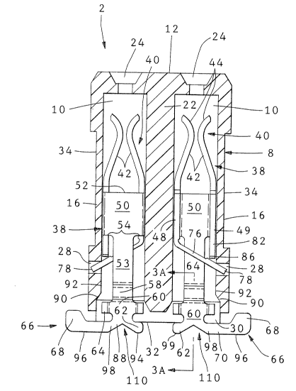
An electrical connector 2 for mounting on a surface
of a circuit board 4 having pads 6 contiguous with traces
7 thereon, comprises an insulating housing 8 defining two
14412 CA -5-
- 1 3 1 0380
~ 7789-275
rows of parallel, terminal receiving, through passages 10 extend-
ing from an upper mating face 12 of the housing 8 to a lower face
14 thereof. The housing 8 has opposed side walls 16 and opposed
end walls 18, the passages 10 of each row being separated from one
another by transverse partitions 20 and the passages of the two
rows being separated from one another by a barrier wall 22. Each
passage 10 opens into the mating face 12 by way of a mouth 24 for
guiding a male electrical contact element 26, one of which is
shown .in Figure 4, into the passage 10. Each passage 10 is of a
rectangular cross section and is elongate perpendicularly to the
faces 12 and 14. There is formed in each side wall 16 in the
vicinity of the lower face 14, a through recess 28 and there
project from the face 14 standoff ribs 30 which extend trans-
versely of the length of the housing 8, there being a rib 30 on
each side of each passage 10. The ribs 30 extend below the face
14 and have a circuit board engaging bottom edges 32. There is
formed in each side wall 16, a longitudinal groove 34 for tool
engagement to contain actuating forces of a hold down. There
projects from each end wall 18, proximate to the face 14, a cradle
36 (Figure 2~ for receiving a hold down or clip (not shown) for
securing the connector to the circuit board 4, for example,
according to the teaching of US-A-4,693,528.
Y`'~
..~ , ~}.
13~0380
An electrical terminal 38 will now be described with
reference to Figure 1. The terminal 38 comprises a mating
portion in the form of a receptacle 40 consisting of
cantilever spring beam contacts 42 having opposed, bowed
5 contact surfaces 44 for gripping between them, a male
contact element 26. The beams 42 extend from a channel
shaped support part 46 of an intermediate portion 47 of
the terminal 38. The part 46 comprises a pair of opposed
side walls 48 and 49 projecting from opposite edges of a
10 connecting web 5S), normally thereof, each beam 42
projecting from an upper edge 52 of a respective one of
the side walls 48 and 49. Edge 52 engages sto~? shoulder
53 in the housing to position terminals 38 upon insertion
into passage 10. The intermediate portion 47 also
15 comprises an elongate, rectangular cross section stem 53
which extends from the lower edge 54 of the web 50 and
which has a rectilinear length 56 connected to the edge 54
and being coplanar with the web 50 and which is connected
by way of a offset 58 bowed in the inward direction of the
20 channel shaped part 46, to a further rectilinear length
60, the end of which remote from the offset 58 is
connected to a planar solder tail 66. Foot 62 also
extends from length 60 and is coplanar with solder tail
66. The foot 62 does not extend to engage pad 6, but
25 ter~ninates a short distance therefrom~ During mating or
board warpage, tail 66 may rotate such that foot 62
14412 CA -7-
1 3 1 0380
engages the printed circuit board or pad 6 to prevent
overstressing a solder joint. Thus, there is a limited
rotation permitted with foot 62 providing an
antioverstress feature. The length 60 has a pair of
opposed bent out lugs 64 extending normally of the plane
of the portion 60 in the same direction as that in which
the offset 58 is bowed. Projecting from the length 60 is
a planar solder tail 66 which is coplanar with the portion
60 and the foot 62 and which extends at right angles to
the longitudinal axi of the terminal 38. The solder tail
66 has an enlarged soldering portion 68 which is connected
to the length 60 by way of a rectilinear arm 70 of said
tail 66. The foot 62 and the tail 66 are formed
integrally with a slug 72 as shown in Figure 1, which is
in turn formed integrally with a carrier strip (not shown)
connecting the terminal 38 to multiplicity of identical
terminals 38 in side by side, parallel, relationship to
provide strip of terminals 38 for application to the
housing 8 by means of an automatic stitching machine (not
shown).
There projects from the lower edge 74 of the side
wall 48, a resilient lance 76 canted obliquely away from
the chànnel shaped part 48 and having a free end 78
located beyond the side wall 49. A length 80 of the lance
76 extending from the edge 74 is of reduced cross section,
having been coined to reduce its thickness by, for
14412 CA -8-
1 31 0380
example, one quarter, for the purpose of improving its
spring properties and its compliance. An elongate StGp
member 82 for the lance 76 extends from the lower edge 84
of the side wall 49 towards the lance 76 and terminates in
a stop face 86 directed towards lance 76.
The terminal 38 and the other terminals of the said
strip can be produced from a single piece of pre-plated
rolled sheet metal stock, for example brass stock of 8
mils in thickness, by means of a progressive die forming
operation in which blanks for the individual terminals,
the blanks remaining connected to the carrier strip
mentioned above, by means of the slugs 72, were stamped
from the stock and formed to the configuration just
described. Thus, the terminal 38 has broad rolled
surfaces and sheared edges. For loading the housing 8
with terminals 38, a stitching machine (not shown) is
employed to shear the slug 72 from each terminal 38 along
a V shaped shear edge 88 forming notch 110 and then to
insert each terminal 38 into a respective passage 10 of
the housing 8 by way of the lower face 14 thereof,
chamfered inner surfaces 90 of the side walls i6 serving
to depress the resilient lances 76 to slide along adjacent
surfacès 92 of the side walls 16 so that upon full
insertion of a terminal 38 the free end portion of the
lance 76 of ths terminal snaps into the respective recess
28. The receptacle 40 of the terminal extends towards the
14412 CA -9-
3 ~ ~)
mating face 12 in alignment with the respective mouth 24,
its foot 62 and soldering tail 66 lying beyond the lower
face 14 and the standoff ribs 30, as shown in Figure 3,
with the soldering portion 68 of the tail 66 lying beyond
the adjacent side wall 16 and thus outside the housing.
The lugs 64 are slidable within passage 10 as seen in
Figures 3 and 4.
The foot 62 ha~ a sheared edge 94, the tail 66 having
a sheared pad engaging edge 96. In the preferred
embodiment, sheared edges 94 and 96 are coplanar. In an
alternate embodiment, sheared edge 96 extends
substantially normal to the longitudinal axis of the
terminal a greater distance from length 60 than sheared
edge 94. By virtue of the slugging out operation, notch
110 is formed and the arm 70 of the tail 66 is conn~cted
to the foot 62 by a reduced cross section neck 98 whereby
the tail 66 can be flexed resiliently, in its own plane
and transversely thereof with respect to the foot 62 and
the sheared edge 99.
In order to mount the connector 2 on the circuit
board 4, the connector 2 is applied to the board 4 with
the feet 62 and tails 66 leading, so that edge 96 of the
tail 66 of each terminal 38 is positiQned against a
respective pad 6. Although the pads 6 are narrow, they
provide sufficient width to solder to the faces of the
tails. Since a sheared edge of the terminal is employed
14412 CA -10-
1 ~ I ()38Q
to maXe electrical contact with the pads 6, the center to
center spacing of terminals 38 may be for example as small
as 0.050. The connector 2 is pressed down on the board 4
until the stand-off ribs 30 engage its surface so that
each terminal 38 is urged against the action of its
resilient lance 76, inwardly of its passage 10, as shown
in F'igure 4, the lances 76 pivoting about their free end
portions in the recesses 28, whereby the sheared edges 96
are resiliently urged against the pad 6 and if arm 70
flexes, sheared edges 94 may engage the printed circuit
board.
The clips having been inserted into the cradles 36,
and the connector installed on the printed circuit board
the sheared edges 96 of the soldering portions 68 of the
tails 66 and the faces thereof are soldered to the
respective pads to provide solder fillets 100 electrically
connecting the portions 68 of the tails 66 to the pads 6
as shown in Figure 4. In order to enable the soldering
operations to be carried out, solder paste is screened on
to the board 4 so as to cover the pads 6 prior to the
application of the connector 2 to the board 4. The solder
paste is reflowed to provide the fillets 100, after the
connector 2 has been fastened to board 4 with clips.
During the soldering operation the solder tails 66 are
caused to maintain con~inuous contact with the pads ~ by
virtue of ths resilient action of the lances 76 in
14412 CA
1 3 1 ~380
combination with the clips, which act not only to this
end, but also to la~ch the terminal 38 in their passages
10. Said resilient action of the lances 76 and the fact
that the solder tail 66 can be resiliently flexed about
their necks 98 ~erve to compensate for the board
malformation or warping. The flexibility of the tails 66
about their necks 98 providss a compliant terminal and
protects the solder tails from damage should the solder
connections between the tails 66 and the pads 6 be
stressed, for example as a result of subsequent warping of
the board ~. The fact that the edges 96 are not plated
surfaces is not critical to the soldering operations. The
feet 62 serve to prevent substantial rotary movement o~
the terminals 38 under mating forces.
Prior to assembly to the board 4, the connector 2 may
be packed in a tube, a tray, or a magazine, together with
other connectors 2, for supply to a customer. The grooves
34 in the side walls 16 of the housing 8 may be used for
rail mounting the connectors 2 in such containers or for a
robotic gripper to self contain ~orces of a top actuated
hold down. The resilient flexibility of the tails 66 also
serves to protect them when the connector is being
handle~, before its assembly to the board 4. The lugs 64
of the terminals 38 prevent excessive rotation of arm 70
thereby providing maximum registration on pads 6. Forward
stop edge 52 engaging shoulder 53 prPvents the terminals
14412 CA -12-
1 3 1 0380
from being pushed into their passages 10 during handling
of the connector 2, to an extent to damage the lances 76.
Stop faces 86 are engageable with the lances 76 to prevent
the terminals 38 from being pulled out of their passages
10 during such handling.
14412 C~ -13-