Note: Descriptions are shown in the official language in which they were submitted.
1 31 03q 1
6~-57,844 comb.
SUPERCONDUCTIVE OPTOELECTRONIC DEVICES
ThiS invention relates to a number of super-
conductive optoelectronic device and a superconductive
optoelectronic apparatus. The superconductive opto-
electronic devices and apparatuses of the invention are
05 novel and vastly different from those of prior art in
that the invention uses a combination of superconductive
material and special superconductive photoconductive-
material which reveals photoconductivity below the
critical temperature of the relevant superconductive
material.
With recent development of superconductive
materials, various new superconductive substances have
been found; for instance, superconductive oxide
materials such as those of Y-Ba-Cu-O system and Ca-Sr-
Bi-Cu-O systems. However t most of current research
effort are focussed on the raising of transition
temperature or critical current, and not much studies
except those on the reflection or scattering have been
made on either optical properties of superconductive
substance or industrial applications of such optical
properties. The reason for it is in that, generally
speaking, researchers have considered that superconduc-
tivity is incompatible with such physical properties as
~jb
- 2-
1 3 1 039 1
optical absorption and photoconductivity and they have
assumed that optical irradiation in the region of an
excess amount of energy with the relevant wave number
beyond the energy gap of the BCS theory will merely
05 destroy the stability of superconductivity. Further,
most o~ the superconductive materials which have been
developed so far are metals or alloys, and no
superconductive materials with useful optical properties
have been found. No concept has existed on a new field
to be called "Superconductive Opto-Electronics"
On the other hand, if high-temperature super-
conductive oxide material are combined with recently
developed superconductive photoconductive-materials
which reveal their proper photoconductivity at temper-
atures below the transition temperatures of the relevantsuperconductive oxide materials, a number of new
electronic devices and optoelectronic apparatuses may be
~eveloped, for instance, a switching device with no
power loss, an optically operating device with no power
2~ loss, an optically operating logical device, a space
parallel type optically operating apparatus, a camera or
an image forming device possibly with superconducting
wiring, a high-speed optically operating apparatus to be
driven at an extremely low power, and the like.
Although most researchers currently aim at the
raising o~ transition temperatures of superconduc~ive
1 31 03~1
materials, the inventor has performed a number of
experiments and analyses on optical properties of super-
conductive oxide materials, such as those of the Y-Ba-
Cu-O and La-Cu-O system, Ca-Sr-Bi-Cu-O system and Ba-Pb-
~ Bi-O system. Consequently, the inventor has discovered
an entirely new and remarkable phenomenon in that some
of the above oxide materials, i.e., superconductive
photoconductive-materials to be defined later, reveal
onsets of photoconductivity at temperatures below the
critical temperature for superconductivity (transition
point) of that superconductive substance which i5
related to the superconductive photoconductive-material.
The superconductive photoconductive-oxide materials are
so far electric insulators at room temperature, but when
they are cooled down to the temperatures below the
transition points of superconductive materials related
to them, they reveal photoconductivity, i.e., they
produce photo-carriers and their conductivity varies
depending on the intensity of the excitation liqht which
is incident thereto.
A power-loss-free useful superconductive opto-
electronic device can be formed by combining a super-
conductive photoconductive-material of for instance the
Ca-Sr-Bi-Cu-O system with its related superconductive
material of for instànce the Ca-Sr-Bi-Cu-O system. What
is meant by "superconductive optoelectronic device" is
1 31 03~1
an optoelectronic device made of a combination of a
superconductive material of one oxide system and that
superconductive photoconductive-material of the same
oxide system which reveals photoconductivity at temper-
~ atures below the critical temperatures of the super-
conductive material.
An object of the invention is to provide a novel
superconductive optoelectronic device by using effec-
tively the optical properties of that superconductive
12 photoconductive-material ~hich is discovered by the
inventor. Thus, the invention is neither a mere
improvement of the prior art nor a simple solution of
problems existing in the prior art, but an entirely new
achievement.
~ superconductive optoelectronic device accord-
ing to the present invention, for instance, comprises a
substrate, a photoconductive gate region formed on the
substrate, and a source region and a drain region formed
on the substrate at opposite sides of the gate region
respectively so as to face toward each other across the
gate region. The source and drain regions are made of a
superconductive material, while the gate region is made
of a superconductive photoconductive-material which
reveals photoconductivity at temperatures below the
critical temperature for superconductivity of the
supercondu~tive material, and the superconductive
1 31 03~ 1
photoconductive-material and the superconductive
material are of the same general chemical formula but
with different contents of constituent elements.
Bias source may be connected across the source
05 region and the drain region o the optoelectronic
devices of the invention, so as to drive an electric
current through its photoconductive gate region depend-
ing on the intensity of light which is incident to the
photoconductive gate region.
Once such a type of superconductive opto-
electronic device is formed, it must be naturally
straight forward to develop the new field from such a
device to other devices, and eventually to superconduc-
tive optoelectronic apparatus, for instance a switching
1~ device with no power loss, an optically operating device
with no power loss, an optically operating logical
device, a space parallel type optically operating
device, a camera or an image forming device possibly
with superconducting wiring, a high-speed optically
operating apparatus to be driven at an extremely low
power, and the like.
For a better understanding of the invention,
reference is made to the accompanying drawings, in which:
Figure 1 illustrates typical graphs showing of
2~ the temperature dependences of photoconductivity Q(T, ~)
and superconductivity in resistivity p~T) of the Ca-Sr-
1 31 0391
Bi-Cu-0 system oxides ceramics at ~~580 mm and with the
data of photoconductivity of the reference substance
Bi203 ceramics at ~~660 mm;
Figure 2 is a graph showing the wavelength
S dependence of the photoconductive response Q(T, ~) of
the Ca-Sr-Bi-Cu~0 system oxides at T~4.2K and with that
of the reference substance Bi203 ceramics at T~77K;
Figure 3 illustrates typical graphs of the
temperature dependences of photoconductivity Q(T, ~) of
io the Cal_x-Yx-Sr2-Bi~-Cu2-Oz system (X=l~ oxide ceramics
at ~ 660nm with the data of the photoconductivity of
Q(T, ~ of the reference substance Bi203 single crystal
at ~~515 nm;
Figures 4 are graphs showing the temperature
1~ dependences of resistivity in the dark of the Cal_x-Yx-
Sr2-Bi2-Cu2-0z system (x=l~0) to display an insulator to
superconductor transition at x~0.6;
Figure 5 ls a graph showing the wavelength
dependences of the photoconductivity Q(T, ~) of the
reference substance Bi203 single crystal at ~~~.2K;
Figure 6 is a graph showing the photoconduc-
tivity Q(T, ~) and superconductivity in resistivity p(T)
of the Y3_x-Bax-Cu3-Oz system oxides including the
photoconductivity of Y3Cu30z (x=0) at ~~480 nm and (b)
26 Y2BalCu30~ (x-l) at ~~570 nm;
Figure 7 is a graph showing the wavelength
- 7-
1 31 03~ 1
dependence of the photoconductive response Q(T, ~) of
the Y3_x-Bax-Cu~-Oz system oxides including that of
Y3Cu30z (x=0) with the data of optical absorption of the
reference substance Cu20 at ~~4.2K;
~ Figure 8 is a graph to show at example of the
relationship between the intensity of excitation light
and photoconductive response of the Y-Ba-Cu-0 system
oxides Y2Cu30z (x=0) at ~~ 470 nm;
Figure 9 is a graph showing the temperature
dependence of photoconductivity Q(T, ~) of the Ba-Pb-Bi-
0 system oxides and at A~580 nm the photoconductivity
of the reference substance Bi203 ceramics at ~~660 nm;
Figure 10 is a graph showing the wavelength
dependence of the photoconductive response Q(T, ~) of
lB the Ba-Pb-Bi-0 system oxides T~4.2K and that of the
reference substance Bi2o3 ceramics at T~77K;
Figure 11 is a graph showing the temperature
dependence of photoconductivity Q(T, ~) and
superconductivity in resistivity p~T) of the La-Cu-0
system oxides;
Figure 12 is a graph showing the wavelength
dependence of the photoconductive response Q(T, ~) of
the semiconductive and superconductive La-Cu-0 system
oxides at T~4.2K with the data of the optical
2~ abosrption of the reference substance Cu20 at T~4.2K;
Figure 13 is a graph to show an example of the
1 31 0391
relationship between the intensity of excitation light
and photoconductive response of La-Cu-O system oxides at
~570 nm;
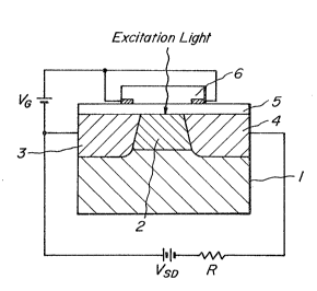
Figure 14 is a schematic sectional view of a
05 superconductive optoelectronic device according to the
invention;
Figure 15 is a schematic partial sectional view
of a superconductive optoelectronic alley device
according to the invention;
Figure 16 is a diagrammatic illustration of a
space parallel optically operating superconductive
optoelectronic apparatus which uses alleys of the
superconductive optoelectronic devices of the invention;
Figures 17 illustrate the concepts of (a) a
"polaron", i.e., a conduction electron or a positive
hole associated with LO-phonons or deformation of host
crystal lattice together in free motion; (b) a
"bipolaron" mediated via a coherent ensemble of phonons
or lattice deformations;
Figures 18 illustrate a schematic form of (a) an
exciton with a wavevector K and transistion moment P,
which sometimes couples with (b) photons with a
wavevector " and the direction of polarization ~;
Figures 19 are schematic diagrams to show the
26 relationship between energy E and density of state N(E~
of (a~ the Ca2_x-S~x-Bi3_y-Cuy-Oz system~ for the cases
~ 1310391
of x=0 (insulator) and x=l (superconductor) and both for
y=2; and (b) Bal-Pb1_x-Bix-Oz for the cases of x>0.35,
x~0.3, 0.2 and x<0.15; and
Figures 20 are schematic diagrams to show the
05 relationship between energy E and density of state N (E) of
(~) the Y3_x-Bax-Cu3-O~, and (b) the La2-Cu1-Oz systems.
Throughout dif~erent views of the drawing in
Figs. 14~16, l is a substrate, 2 a gate region, 3 a
source region, 4 a drain region, 5 an insulating layer,
6 a conductive glass layer, 10 an alley-like light
source, ll a coding image-mask pattern, 12 a correlative
image screen, and 13 is a decoding mask optical element
alley.
The inventor's experiments and analyses on the
1~ photoconductivity and superconductivity of various
~uperconductive materials showed that a certain portions
of superconductive materials in their phase diagram
reveal photoconductivity complementary to or as well as
superconductivity at temperature below their regions of
transition temperatures from normal conductivity to
superconductivity. For instance, in the case of
superconductive oxides of the Ca-Sr-Bi-Cu-O system, the
inventors discovered that with changing Sr content their
superconductivity can be converted into photoconduc-
2~ tivity at temperatures below their cxitical temper-
atures.
- 10 -
1 3 1 03q 1
Figure 1 illustrates typical results of
experiments on the superconductivity and photoconduc-
tivity of the Ca-Sr-Bi-Cu-O system oxides. The curve
(a) in Fig. 1 shows the temperature dependence of
05 photoconductivity of Bi2O3 ceramics which is a reference
substance clarified by the inventor. The curve (b) in
FigO 1 illustrates the temperature dependence of
superconductive photoresponse of Ca2-x-srx-Bil-cu2-oz
(x=0). The curve (c) in Fig. 1 illustrates the
temperature dependence of electric resistance of
Ca2_x-Srx-Bil-Cu2-O~ (x=l) in the dark. After a number
of experiments and analyses on the Ca-Sr-Bi-Cu-O system
oxides with a general chemical ormula of
Cam_x-Srx-Bin y~Cuy~Ozr the inventors found that, under
the conditions of
2~m~4, 35n55, OsxS2, 15yS3, 4~zSll,
if the content x of Sr is between 1 and 2, i.e., 1Sx~2,
the oxides reveals superconductivity, while if the
content x of Sr is not more than l,i.e., Osx<l, the
oxides reveals photoconductivity.
More particularly, with m=2, n=3, y=2 under the
above-mentioned conditions, the Ca-Sr-Bi-Cu-O system
reveals superconductivity if, e.g., its content x of Sr
is in the range of 0.7~1~x~2, and if its content x of Sr
is smaller than 0.7~1 such superconductivity disappears
and it reveals complementary photoconductivity at
131~391
temperature regions below their transition temperatures.
Those ma~erials whose superconductivity is converted
into complementary photoconductivity and vise versa
depending on the concentration of a part of their
~ ingredient atoms at temperature regions below their
transition point temperatures will be referred to as
"superconductive photoconductive-materials" and their
property will be referred to as "superconductive
photoconductivity" herein.
Curves (a) and (b) in Fig. 2 display wavelength
dependence of photoresponse of the reference substance
and the oxide specimen Bi2O~ ceramics at T~77R and
Ca2_x-Srx-Bil-Cu2-Oz (x-0) at 4.2 K, respectively.
The reference substance Bi2O3 ceramics and the oxide
Ca2_~-Srx-Bil-Cu2-O~ (x=0) have similar wavelength
dependence~; more specifically, as the wavelength
decreases from 650 nm, their photoresponse Q (T, ~)
gradually increases, whereas their photoresponses remain
substantially at low levels for wavelengths longer than
650 nm. The inventors noted that if a material revealing
photoconductivity at a temperature below its transition
temperature is combined with another material revealing
superconductivity at a temperature below its transition
temperature, then such a combination will provide a
2~ useful superconductive optoelectronic device which
xeveals both superconductivity and photoconductivity at
1 31 03ql
a temperature below the transition temperature thereof.
More specifically, if an optoelectronic element
of FET-like shape is formed by making a gate region with
a superconductive photoconductive-material while making
0~ a source region and a drain region with a relevant
superconductive material, an output current whose
magnitude varies depending on the wavelength and
intensity of light incident to the gate region can be
produced so as to flow across the source and drain
regions. If such an optoelectronic device is sustained
at a temperature below the transition temperature of its
superconductive material, it must work as a
superconductive optoelectronic device which can be used
in numerous ways; for instance, as a power-loss-free
16 optical switching device with high-speed response, an
optical detector, an optical signals amplifying device,
or the like.
In order to obtain more systematic knowledge on
the characters of material systems in a series of
compositions, e.g., the effect of the composition on the
variations of lattice constants in a crystal structure,
the inventor has studied also the ~Ca1 xYx)Sr2Bi2Cu2Oz
system to obtain data especially from the view point of
photoconductivity complementary to superconductivity
26 together with new data of the reference substance Bi2O3
single crystals. [Characteristic features of this
- 13-
1 31 03ql
series of system such as the variations of lattice
constants, electrical resistivity in the dark and a
magnetic susceptibility with varying x have been studied
in details by T. Tamegai et al. Jpn. J. Appln. Rhys. 27
06 L1074 (1988) and T. Tamegai, Parity Vol.3, No. 11, 43
(1988) (in Japanese).] The single crystals of Bi2O3
have been grown for the first time in the inventor's
laboratory.
Figure 3(a) and (b) illustrate typical traces of
the temperature dependences of photoconductivity signals
Q (T, A) of the reference substance Bi2O3 single ~xystal
and of the Cal-xYxSr2Bi2Cu2Oz (x=l) specimen of oxide
ceramics, whereas Fig. 4(a) and (b) show the temperature
dependences of resistivity in the dark of the
1~ Cal_xYxSr2Bi2Cu2Oz system (x=l~0) to display an insulator
to superconductor transition between x~0.55 and x~0.6.
With these data, one can definitely recognize
even another more systematic series of material
Cal_xYxSr2Bi2Cu2Oz also exhibits an emergence of
superconductive photoconductivity at x-l, but rather
low temperature T~ 20K . In Fig. 5, the graph displays
the wavelength dependences of the photoconductivity
Q (T~ ~) of the reference substance Bi2O3 single
crystal. This is not necessarily inconsistent with the
data in Fig. 2(a)~ since thickness of specimens and
proportion of the surface to volume ratio are different
- 14-
1 31 03~1
from each other.
Oxide material of the Y-Ba-Cu-O system will be
described now by referring to Fig. 6 which shows test
results on its superconductivity and photoconductivity.
05 The curve (a) in Fig. 6 shows the temperature dependence
of photoresponse ~ (T, ~) of Y3_x-Bax-cu3-oz (x=0), the
curve (b) shows the temperature dependence of photo-
response Q (T, ~) Of Y3_x-Bax-cu3-oz (x=l), and curves
~c) in Fig. 3 show the temperature dependence of dark
resistivity of two specimens oE Y3-X Bax-Cu3-Oz (x=l,
x=2). In the case of Y-Ba-Cu-O system oxides with a
~eneral chemical formula Of Y3~x-Bax-cuy-ozt their
superconductivity is converted into photoconductivity
depending on both the content x o~ Ba and the content z
16 of oxygen. Under the conditions of
lSx~2 and 6.5~z~7,
the oxides reveal superconductivity, while under the
conditions of
05x~1 and 7.05z~7.5, or x-2 and 6.0~z<6.5,
the oxides reveal photoconductivity at temperatures
below their transition temperatures. Here, z< 6.5 is a
merely rough indication of the boundary not clearly and
should not be taken exactly, since the superconductive
defined photoconductive-area are continuously close to
2~ the superconductive-areas in thier phase dia~ram.
Similar situations are the cases also for the other
1 31 03~1
systems as far as the oxygen content z concerns.
As can be seen from the curves ~a) and (b) in
Fig. 6, the two specimens Of Y3_x-Bax-cu3-oz (x=0, x=l)
clearly reveal superconductive photoconductivity at
06 temperatures below their transition temperatures.
Fig. 7 shows the dependence of photoconductivity
Q(T, A) of the above Y-Ba-Cu-O system oxides on the
wavelength ~ of excitation light at a temperature
T=79 K. As can be seen from Fig. 7, the oxides reveal
intrinsic photoconductivity at a temperature below their
transition temperatures in response to excitation light
with wavelength at ~-420-640 nm. Fig. 8 shows the
dependence of the photoconductivity of the similar oxide
(x=0) system on the intensity of excitation light at a
wavelength ~=470 nm. It may be concluded from Fig. 8
that photoresponse signals Q (T, ~) of the oxide
material of Y3_x-Bax-cu3-oz system increases with the
intensity of the excitation light. The inventors found
that the Y3 x-Bax-Cu3-Oz system oxide becomes a super-
conductive photoconductive-material when its Ba concen-
tration x is in a range 0~x~l, while it becomes a
superconductive material for l~x~2.
Oxide material of Ba-Pb-Bi-O system will be
described now by referring to Fig. 9 and Fig. l0.
Curves (a) and (b) in Fig. 9 show the temperature
dependences of photoresponse Q (T, ~) of a reference
-16-
1 31 03ql
substance Bi2O3 ceramics and oxide specimens with a
general chemical formula of Bal-Pbl_x-Bix-Oz, respec-
tively. Curves (a) and (b) in Fig. 10 show the
wavelength dependences of such photoresponse Q (T, ~) of
OS the reference substance Bi2O3 ceramics and the above
specimens Bal-Pbl_x-Bix=Oz (x-0.5), respectively. In the
case of the oxides with a general chemical formula of
Bal-Pbl~x-Bi~-Oz, the inventor found that they reveal
superconductivity under the conditions of
0.2osxsoo35 and 2.81~z~3,
while they reveal photoconductivity under the conditions
of
x20.35 and 2.7~z~2.81.
Referring to Fig. 11 through Fig. 13, oxide
material of the La2-Cul-Oz system will be described now.
Curves (a) and (b) in Fig. 11 show the temperature
dependence of photoresponse Q (T, ~) of the oxide for
cases of ~=3.88 and z=3.92, respectively. Curve (c) in
Fig. 11 shows the temperature dependence of resistance
of the oxide in the dark for both z=3.88 and z=3.92.
It has been known that La2-Cul-Oz system oxide with
z23.9~ reveals superconductivity at a temperature below
about 30 K. The inventors found that if the oxygen
concentration of such oxide is reduced, its super-
2~ conductivity is converted into photoconductivity asshown in Fig. 11. It was also found that the oxide
1 31 03ql
reveals photoconductivity over a wavelength range of
~450-650 nm as shown by curve (b) (for z=3.88) and
curve (c) for (z~3.92) in Fig. 9. Fig. 13 shows the
relationship between the photoconductivity and the
05 quantity of incident light (iOe~, excitation light
intensity) for the above oxide with z~3.88. It can be
seen from Fig. 13 that the photoresponse current clearly
increases with the intensity of incident light~
r Examples ]
1~ Fig. 14 is a schematic diagram showing the
structure of an embodiment of the superconductive
optoelectronic device according to the invention.
The embodiment is a superconductive phototransistor in
which a positive gate voltage VG is used (VG20).
1~ A substrate 1 is made of SrTiO3, and a photoconductlve
gate region 2 is formed on the substrate 1 with super-
conductive photoconductive-material Ca2-Bil-Cu2-Oz.
The photoconductive gate region 2 has a width of 0.2 ~m
to 1.0 mm and a thickness of 1-10 ~m. The above super-
conductive photoconductive-material Ca2-Bil-Cu2~Oz
reveals p~otoconductivity in response to excitation by
incident light of wavelength at least ~~540-740 nm at a
temperature below the transition temperature of a
superconductive substance Cal-Srl-Bil-Cu2-Oz.
At opposite portions over the gate region 2, a source
region 3 and a drain region 4 are formed with
- 18-
1 :~ I (J3~ 1
Cal-Srl-Bil-Cu2-Oz oxide which reveals superconductivity
below its critical temperature of ~OK or 105-115 K.
An electrically insulating layer 5 which is optically
transparent is formed so as to cover top surfaces of the
~ gate resion 2, the source region 3, and the drain
region 4. The insulating layer 5 of the illustrated
example was a 1 ~m thick SiO2 film or mylar sheet.
Further, a conductive surface of glass layer 6, for
instance made of a NESA (Trademark of Pittsburgh Plate
Glass Company) glass layer, is placed on the insulating
la~er 5, and electrodes are deposited on the conducti~e
surface of glass layer 6.
A source for bias voltage VG is connected across
the source region 3 and electrodes of the conductive
surface of glass layer and a source for source-drain
voltage VSD is connected between the source region 3 and
the drain region 4 across the gate region 2.
In preparation of the source region 3 and the
drain region 4, it is also possible even to form a
comparatively broad region of Ca2_x-Srx~Bil-cu2-oz (x=O)
at first and then change continuously the concentrations
of Ca and Sr so as to produce a gradual concentration
change from x=O to x=l in the broad region only at both
sides.
In operation, the superconducting optoelectronic
element of Fig. 14 is cooled to a temperature below the
- lg -
1 3 1 03q 1
critical temperatures, i.e., about 80K or 105-115K, of
the superconducting zones of Ca2_x-Srx-Bil-Cu2-Oz and
excitation light signals in a wavelength range is
irradiated to the gate region 2. A pulaed dye ~aser of
~ 3 nsec width can be used for an excitation light source.
This fact basically indicates a high speed response of
the device itself. Thereby, photocarriers are generated
in the gate region 2 depending on the photon number or
intensity of light incident thereto. The generated
carriers are accelerated by the source-drain voltage VSD
so as to produce an induced output current which is
delivered to an output resistor R. Accordingly, an
output voltage due to incident photosignals appears
across the resistor R.
1~ The amount and density of optically excited
carriers in the gate region 2 can be variable depending
not only on the photon number or intensity of incident
light thereto but also the bias voltage VG~ and the bias
voltage VG can ~e harmoniously adjusted so as to meet
specific requirements from users . By selecting an
appreciate wavelength ~ for excitation light,
photocarrier density of the order, e~g., of 10l2/cm3 can
be obtainable in a surface layer of the gate region 2.
With the above output current characteristics depending
on the intensity of incident light, the superconducting
optoelectronic device of Fig. 14 can be used as a
- 20-
13103ql
superconductive switching device. The source region 3
and the drain region ~ made of ~uperconductive material
are free from heat genexa~ion during operation, so that
the optoelectronic device of Fig. 14 possesses those
OG advantages which are inherent to superconductivity.
Fig. 15 is a partial schematic diagram of an
embodiment of the superconductive optoelectronic device
of the invention, in which device a number of th~ -
superconductive optoelectronic devices of Fig. l~ are
integrated at a high density in the form of one- or two-
dimensional alleys. If wiring among different devices
in the device of Fig. 15 is made by using supercond~ct-
ing material, heat generation in the alley or apparatus
can be suppre~sed to an extremely low level.
1~ The superconducting optoelectronic device and apparatus
of the invention can be used in various fields; for
instance, as a loss-free picls up (or camera) devices,
loss-free detectors o optical signals in an optical
computer which executes parallel operations in a
spatially arranged manner, and the like. The device of
the invention can be also used in a multiple channel
system which selectively utilizes a number of different
wavelengths in the incident light.
Fig. 16 schematically illustrates an optical
calculation procedure in a projection-correlative
optical system of a space parallel optical computer in
- 21 -
131~3ql
~hich system ~lle superconductive optoelectronic devices
of the illven~ioll are used. As alley-like light source lO
projects ~ number of optic~l operation signals in parallel
onto an encoded rnask pattern ll. ~ne mask pa-t-tern 11 car~-ies
o~ encoded image signals in a mask fashion, which signals
respond to the ~ype of operation to be carried by io
the light beams. A~er passing through the mask pattern
ll, th~ light beams pass a correla~ive image screen 12
and then enter in parallPl iIltO the corresponding
10 devices in a decoding maslc optical device alley 13.
Each optical device receives a coded signal which is
modulated by the screen mask, and operated results can
be obtained from the optoelectroIlic output signal~ ~rom
each o~ the optical devices. If each op~ical deviee of
1~ the decoding mask optical device alley 13 is the
superconductive optoelectronic device of the invention,
parallel optical operations can be ef~ectecl while
minimizing heat generation during the operation.
Although the invention has been described so far
by re~erring to an embodiment in the ~orm o~ three-
terminal clevice, the superconductive optoelectronic
device oE the invention can be also made in the form of
a two-terminal device. More particularly, carriers
generated under the condition of VG=O in a broad gate
2~ region are influenced by the superconductive proximity
effect due to superconductive photoconductivity
-2~-
'~3
1 3 1 03~ 1
irrespective of a small coherence length, and one can
expect that the superconductive optoelectronic device of
the invention may be used as a superconductive Josephson
~unction device based on light irradiation. Thus, such
06 two-terminal device may be treated as a "superconductive
photoconductivity or optically controlled Josephson
junction device". In this case, the gate width and the
intensity of the incident light must be properly
selected.
The illustrated embodiment of the invention is
made by using the Ca-Sr-Bi-Cu-O system oxides~ but other
superconductive photoconductive-materials such as those
of the Ba-Pb-Bi-O system, La-Cu-O system, or Y-Ba-Cu-O
system can be also used to form the superconducting
optoelectronic device and apparatus of the invention.
For instance, a superconducting optoelectronic device
which is similar to the embodiment of Fig. l4 can be
made by forming the gate region with Ba1-Pbo.s-Bio s-O3,
while forming the source region and the drain region
with Bal-pbo.7s-Bio. 25-3 -
[Discussion]
The detailed mechanism of the above photo-
conductive phenomenan of the superconductive photo-
conductive materials have not been fully clarified yet,
but the inventor assumes it on the basis of the concepts
of "polarons and excitions as ~ollows. A polaron is a
- 23 -
1310391
freely moving conduction electron or a positive hole
associated with LO-phonons or latice deformations or
even more generally with electronic polarization as
schematically illustrated in Fig. 17(a). There is also
~ even a concept of "bipolaron" due to coherent electron-
phonon intraction or electron-electron correlation
effects as illustrated in Fig. 17(b).
An exciton is an entity of elementary excitation
as depicted in Fig. 18(a~ which consists of a conduction
electron and a positive hole bound together in an atomic
hydrogen-like manner, sometimes, hybridized with (b)
phonons to compose a "polariton".
The spectral response or photoresponse signal
Q(T, ~) of the curves (a) and (b) of Fig. 2 implies that
there exist such parts in the specimen of
Ca2_x-Sr~-Bi3_y-Cuy-Oz system oxide which are similar to
Bi2O3 in an atomic sense, e.g., the (Bi2O2)2~ layer.
The phenomena oE optical absorption and photoconduc-
tivity of Bi2O3 have been clarified even only in part
neither by experiments nor by the exciton theory.
However, it is probably a typical example of Frenkel
type exciton that is related to and associated with
mobile charge in cation shell. The positions of the
fine structures in the Q(~, T) in Fig. 2 basically
a~ coincide with those of the fundamental absorption edge
in Bi2O3 itself. We can recognize a few prominent fine
- 24-
13~0391
structures probably due to the excitons, e.g.,
structures around A~623 nm in the photoconductivity
spectra of Ca2-Bil-~u2-O3 similar to those of Bi2O3
ceramics structure of which appear to correspond to the
05 n~2 state in a certain series of excitons of Bi2O3.
Thus, we may reasonably conceive that there exists at
least a finite fraction of the Bi2O3-like part or phase
which cannot be ignored in the Ca-Sr-Bi Cu-O system
substance, where the photoexcited electrons and holes
10 are definitely mobile, irrespective of a certain
difference of the crystal structures and the density of
states. (See Fig. 19 (a))
A conduction electron or a positive hole in
standard types of Bi2O3 or Cu2O crystals has been
1~ reported to form a rather small or large polaron,
respectively. However, an onset of "photoconductivity"
Q(Ar T3 even in the insulating specimens is clearly
associated with an onset of "superconductivity" as if
the superconductivity potentially underlies the
photoconductivity phenomenon or vice versa. Thus, as to
the effects of a polaronr whether it is a large polaron
due to interaction with the LO-phonons, a small one due
to the Jahn-Teller effect or possibly an intermediate
one due to both effects, the effects of a polaron must
2~ be at least potentially important as indicated in Fig. 1
through Fig. 13, as well as "the electronically
1 ~ 1 03q 1
polarized polaron effect". They are probably effective
in a coherently hybridized form of elementary excita-
tions. Here, we must pay special attention to the
electronically polarized polarons, which one may call an
05 "excitonic polaron". No one can fail to recognize close
association among polarons and excitons with the
experimental data here.
As shown in Fig. l9 (a), these polarons and
excitons in the Ca-Sr~Bi-Cu-O system had yielded out of
the optical interband transition from the hybridized
oxygen-(2p) and 8i-(6s) valence bands mainly to the Bi-
(6p) conduction band together with the LO-phonon
interaction, while leaving 0(2p)6Bi(6s)l "holes"
(represented by a white circle) and creating a Bi(6p)
conduction electron. ~owever, a polaron in the
Ca-5r--Bi-Cu-O syste~ substance can be created either by
the optical excitation or substitution of Ca with Sr
perhaps via a chemical pressure. (See Fig. l9 (a) x=O
and (b) x=l). In this case, the substance becomes
supercohductive at x=l.) Since the positive holes in
the hybrid Bi(6s) and 0(2p) bands can be created from
the many-body ground state by either an intra- or inter-
band transition, the electron correlation effects
naturally important. One must pay more attention to the
dynamical valence fluctuation between Bi3+ and Bi5~ and
especially between Cul+and Cu~, as well as between Bi3
- 26-
1 3 1 03q 1
and Bi4~ and between Cu2~ and CU3+. Therefore, for the
mechanism of high~temperature superconductivity, we may
reasonably conceive potential roles of an ensemble of
polarons, whether large or small, and especially closely
06 associated excitons~ The ensemble of united polarons
and excitons here are probably a set of bipolarons,
polaronic excitons and/or, most probably, "exciton-
mediated bipolarons" due to the dynamical electron-
phonon and electron correlation effects.
The photoresponse signals Q(T, ~) of Ca-Sr-~i-
Cu-O system substance as depicted by the curve (b) in
Fig~ 2 are very similar to those of Bi2O3 ceramics of
the curve (a) in Fig. 2. Consequen~ly, we beliPve that
these studies of elementary excitations here must reveal
1~ the nature of superconducting ground state, irrespective
of an enormous difference in carrier density. In both,
the an excited state via elementary excitation
(insulator) in FigO 19 (a) and the ground state
(superconductor) in Fig. 19 (b), one can expect
occurrence of similar phenomena to those of the
Josephson effect. Similar situations must be the cases
also for the Ba-Pb-Bi-O, Y-Cu-O, Y-Ba-Cu-O, La-Cu-O
systems but with other reasoning as suggested in
Fig. l9(b) and Figs. 20(a) and (b)o
2~ To the best of our knowledge, this is the first
clear experimental indication of the polaron and exciton
- 27-
1310391
mechanisms displayed in the high-temperature super-
conductivity of Ca-Sr-Bi-Cu-O, Ca(Y)-Sr-Bi-Cu-O, Y-Cu-O,
Y-Ba-Cu-O, Ba-Pb-Bi-O, and La-Cu-O system substances.
[Effect of the Invention]
05 As described in detail in the foregoing, a
superconductive optoelectronic device according to the
invention comprises a source region, a drain region, the
two regions being made of superconductive material, and
a gate region made of 'Isuperconductive photoconductive-
10 material" revealing photoconductivity at a temperature
below the transition temperature of the above
superconductive material. Thus, the invention provides
an optoelectronic device with intrinsic "superconductive
properties", i~e., extremely low generation rate of heat
such as Joule heat during operation, and it facilitates
development of various novel superconducting devices
such as "an optically controllable superconductive
Josephson junction devices" and "superconductive
phototransistors".
Further~ a two-dimensional alley-like device
with a high density integration of the superconductive
optoelectronic devices of the invention has such
electrodes and lead wire terminals which are of perfect
diamagnetism, so that it is free from noises and
2~ interferences due to mutual electromagentic induction
~etween adjacent devices or due to outside magnetic
- 28-
1 3 1 ~3~ 1
fields. Therefore, the invention enables production of
an ideal "superconductive optoelectronic device or
apparatus" which operates under optimal thermal and
electromagentic conditions, such as a space parallel
05 optical computer with a very high operating speed.
In short, the present invention is a pioneer in
novel scientific field of "Superconductive Opto-
Electronics".
Although the invention has been described with a
10 certain degree of particularity, it must be understood
that the present disclosure has been made only by way of
example and that numerous variations in details may be
resorted to without departiny from the scope of the
invention as hereinafter claimed.
2B
- 29-