Note: Descriptions are shown in the official language in which they were submitted.
~3~
36~8
--1--
BACKGROUND OF T~E INVENTION
1. Field of the inventlon:
This invention relates to an optical memory
device by which at least one of the information
recording, reproducing, and erasing operations is
carried out by the use of a laser beam.
2. Description of the prior art:
In recent years, various research and
development efforts have been made in many fields to
meet the increasing demand for optical memory devices
of high density and large capacity~ Particularly, an
add-on memory with which the user can add information
and an add-on and erasable memory with which the user
can add in~ormation and erase the recorded information
have a wide range of applications, and accordingly a
variety of materials and systems have been proposed for
these types of optical memory devices. TeOx, TeSe,
TeC, etc., can be used as a material of the former
memory, while a thin film made of a rare earth
transition metal alloy such as GdTbFe, GdTbDyFe,
TbFeCo, etc., can be used as a material for the latter
memory. However, these materials for a recording
medium that is an essential component of the add-on or
the add-on and erasable memory lack in corrosion
resistance and are easily oxidized. The oxidization of
the recording medium results in diminished recording
sensitivity. To overcome this problem, an optical
memory device with add-on memory performance shown in
Figure 8 has been proposed in which on a transparent
substrate 1, a recording medium layer 2 and a
protective layer 3 for protecting the recording medium
3648
-2-
layer 2 agains~ corrosion based on oxidization or the
like are disposed in that order. The recordin~ medium
layer 2 is formed by the vacuum evaporation method, t~e
sputtering method or the like. An optical memory
device with add on and erasable memory performance
shown in Figure 9 has been proposed in which a
transparent substrate 1, a protective layer 3, a rare
earth transition metal alloy thin layer 2, and a
protective layer 4 are disposed in that order. ~nother
optical memory device with add-on and erasable memory
performance that is shown in Figure 10 has been also
proposed in which a reflective layer 5 is further
disposed on the protective layer 4 of the memory device
shown in Figure 9. However, the protective layers 3
and 4 cannot prevent corrosion due to oxidization.
Oxidization of a magneto~optic memory device
(i.e., an optical memory device with add-on and
erasable memory performance) is described below:
Figure 11 shows a conventional magneto-optic memory
device investigated by the inventors of the present
invention, in which on a glass substrate 6, a first
transparent dielectric protective layer 7 with a
thickness of 120 nm of SiO, a rare earth transi-tion
metal alloy thin layer 8 with a thickness of 15 nm of
GdTbFe, a second transparent dielectric protective
layer 9 with a thickness of 50 nm of SiO2, and a
reflective layer 10 with a thickness of 50 nm of Cu are
disposed in that order. This magneto-optic memory
device was subjected to a high-temperature and high-
moisture treatment, resulting in oxidization of the
GdTbFe alloy layer 8. The inventors of the present
invention have recognized that the oxidization is
13~ 3648
caused by oxygen contained in the SiO layers 7 and 9;
oxygen sep2rates from the SiO2 layers 7 and 9 while or
after the said SiO2 layers are formed, and the oxygen
released oxidizes the GdTbFe alloy thin layer 8. Since
oxidi7ation or the rare ear~h transition metal alloy
tnin layer 8 seriously impairs the performance of the
magneti~ed recording medium, oxidization is a serious
problem for optical memory devices. In a case ~here
the thic~ness of the rare earth transition metal alloy
thin layer 8 is small, even though negligible
oxidization arises, the oxidization gives a large
influence, and thus must be avoided with the greatest
care. Accordingly, tAe applicant cr this patent
application has proposed to use aluminum nitride or the
like with no oxygen content as a protective film for
protecting the rare earth transition metal alloy thin
layer 8. An optical memory device with such con-
struction i5 disclosed in European Patent Publication
No. 0 111 988, entitled
"MAG~ETO-OPTIC MEMORY DEVICE" by Xenji OHTA et al.
However,
aluminum nitride mismatches with rare earth transition
metal alloy layers, and the production conditions of
the aluminum nitride layer must be closely controlled
in order to obtain a superior recording medium.
Moreover, the aluminum nitride layer has a high thermal
conductance, and is in~erior in the sensitivity for
recording on the recording medium. The aluminum
nitride layer has a low C/N ratio, and bits cannot be
recorded at a low power level. To overcome these
~ ~ 3~0~ 3648
--4--
problems, C~nadian Patent No. 1,264,852
proposes a protective layer made o~ aluminum nitride
and silicon, which cannot provide a sufficient protec-
tive laver pe ff ormance.
SUMMARY OF THE INVENTlON
The optical memorv device o~ this invention,
which overcomes the above-discussed and numerous other
disadvantages and deficiencies of the prior art,
comprises a substrate, a recording medium layer, and
one or more protective layers for protecting said
recording medium layer, wherein at least one of said
protective layers is made of aluminum tan~alum nitride.
In a preferred embodiment, the recording
medium layer and the aluminum tantalum nitride layer
are disposed on said substrate in such a manner that
the sensitivity of the magneto-optic recording can be
enhanced and the change in the recorded bit length at
the time of changes of the recording laser power can be
reduced.
In a preferred embodiment, the aluminum
tantalum nitride layer is represented by the formula:
(Al1_xTax)~l_y wherein O<x~O.1 and y=0.5.
Thus, the invention described herein makes
possible ~he objectives of (1) providing an optical
memory device that has a recording medium reliable in
resistance against oxidization by oxygen; and
(2) providing an optical memory device that has
.
3648
--5--
excellent information-recording and reproducing charac-
teristics.
BRIEF DES~RIPTION OF THE D~AWINGS
This invention may be better understood and
its numerous objects and advantages will become appar-
ent to those skilled in the art by reference to the
accompanying drawings as follows:
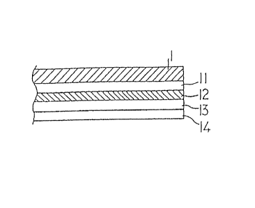
Figure l is a sectional view showing an
optical memory device of this invention.
Figures 2a and 2b are of magnetic character-
istic curves showing the relationship between the
external magnetic field and the Kerr rotational angle
with regard to a reference optical memory device and
the optical memory device of Figure 1.
Figure 3 is a sectional view showing another
optical memory device of this invention.
Figure 4 is a sectional view showing another
~5 optical memory device of this invention.
Figure 5 is a sectional view showing another
optical memory device of this invention.
Figure 6 is a sectional view showing another
optical memory device of this invention.
36~8
~6-
Figure 7 is a sectional view showing another
optical memory device of this invention.
Figure 8 is a sectional view showing a
conventional optical memory device.
Figure 9 is a sectional view showing another
conventional optical memory device.
Figure 10 is a sectional view showing another
conventional optical memory device.
Figure 11 i~ a sectional view showing another
conventional optical memory device.
Figure 12a is of characteristic curves
showing a relationship between the laser power and the
C/N ratio with regard to the optical memory device
shown in Figure 1.
Figure 12b is of characteristic curves
showing a relationship between the laser power and the
bit length with regard to the optical memory device
shown in Figure 1.
Figure 12c is of characteristic curves
showing a relationship between the laser power and the
bit length distribution with regard to the optical
memory device shown in Figure 1.
Figure 12d is of characteristic curves
showing a relationship between the external magnetic
field and the C/N ratio with regard to the optical
~ 3 .~ 3 l~3
364
--7~
memory device shown in Figure 1.
Figure 12e is of characteristic curves
showing a relationship between the external magnetic
field and the bit length with regard to the optical
memory device shown in Figure ~.
Figure 12f is of characteristic curves
showing a relationship between the external magnetic
field and the bit length distribution with regard to
the optical memory device shown in Figure 1.
DESCRIPTION OF THE PREFERRED EMBODI~ENTS
Figure 1 shows an optical memory device of
this invention, which comprises a transparent
substrate 1 made of glass, polycarbonate resins,
acrylic resins or the like, a first transparent
dielectric layer 11 of aluminum tantalum nitride,
(Alo 95TaO 05)0 5No 5, a rare earth transition metal
alloy thin layer 12 of GdTbFe, GdTbDyFe, TbFeCo or the
like, a second transparent dielectric layer 13 of
aluminum tantalum nitride, and a reflective layer 14 of
AlNi in that order. The composition of the aluminum
tantalum nitride layer 11 can be represented by the
formula, (Al1_~Tax)yNy wherein O<x~O.1 and y=0.5.
Table 1 shows the refractive index of the aluminum
tantalum nitride layer 11 when the value x is changed
in the range of O to 0.05. The aluminum tantalum
nitride layer 11 was formed by the RF (radio frequency)
magnetronsputtering method using an aluminum/tantalum
alloy target that was prepared by the melting method,
~ 3 :~ v ~ ~ ~
3648
--8--
wherein a substrate was placed within a RF reactive
sputtering apparatus, the inside of which was then
maintained under a pressure of 1 x 10⁻⁶ torr, and a
sputtering gas containing Ar and N2 ~the gas pressure
ratio of Ar to N2 being 1) was supplied to the
apparatus at a flow rake of 30 standard cubic
cm/minutes undPr a sputterlng gas pressure of 2 m torr.
An RF voltage of 500 W was applied to the target.
Table 1
Values of x Refractive index of the
(All-xTax)0.5N0.5 layer
0.00 2.03
0.01 2.05
_
0.02 2.07
0.03 2.07
0.04 2.07
0.05 2.07
It can be seen from Table 1 that the
incorporation of Ta into the dielectric layer increases
the refractive index of the dielectric layer, which
results in an increase in the magneto-optical effect
(i.e., the Kerr rotational angle).
~ 3 ~ 3648
_g _
A disc of the above-mentioned optical memory
device with a rare earth transition metal alloy thin
Y of (GdO.58Tb0.42)o.27Feo 73 was used to
determine ths C/N ratio, the bit length and the bit
length distribution by changing the write laser power
and the external magnetic field under the conditions
where the laser wavelength is 780 nm, the numerical
aperture of an object lens is 0.6, the linear velocity
of the disc is 5.6 m/sec., and the read laser power is
1 mW. The results are shown .in Figures 12a to 12f.
Figure 12a shows the change in the C/N ratio
at -the time when the write laser power is changed,
which indicates that the transparent dielectric layer
of AlNTa exhibits a higher C/N ratio than that of AlN
even at a low write laser power level. Figure 12b
shows the change in the bit length at the time when the
write laser power is changed, which indicates that the
transparent dielectric layer of AlNTa exhibits a
smaller change of the bit length than that of AlN at
the time of changes of the write laser power. This
means that bits can be recorded with a stabilized bit
length. Figure 12c shows the bit length distribution
at the time when the write laser power is changed,
which indicates that the transparent dielectric layer
of AlNTa exhibits a smaller bit length distribution
than that of AlN; that is, with an AlNTa layer, the
scatter of bit length is so slight that bits can be
stably written even at a low laser power level.
Figure 12d shows the change in the C/N ratio at the
time when the external magnetic field is changed, which
indicates that the transparent dielectric layer of
~ 3 ~
36~8
-10-
AlNTa exhibits a higher C/N ratio than that of AlN.
Figure l~e shows the change in the bit length at the
time when the external magnetic field is changed, which
indicates that the transparent dielectric layer of
AlNTa exhibits a smaller change of the bit length than
that of AlN at the time of changes of the external
magnetic field. This means that bits can be recorded
with a stabilized bit lenyth. Figure 12f shows the bit
length distribution at the time when the external
magnetic field is changed, which indicates that the
transparent dielectric layer of AlNTa exhibits a
smaller bit length distribution than that of AlN at the
time of changes of the external magnetic field.
The above-mentioned optical memory device has
the following advantages: (1) Aluminum tantalum nitride
is extremely stable and can be made into a finer layer
than oxides; (2) Aluminum tantalum nitride that
contains no oxygen as a component can remarkably reduce
the possibility of oxidization of the recording medium
layer; and (3) Aluminum tantalum nitride matches with
rare earth transition metal alloy layers, resulting in
excellent magnetic characteristics as shown in
Figures 2a and 2b wherein the axis of ordinate
indicates the Kerr rotational angle (0.1 /cm) and the
axis of abscissa indicates the external magnetic field
(l kOe/cm). Figure 2a shows the change in the magnetic
characteristic with regard to a reference optical
memory device in which aluminum nitride is used instead
of aluminum tantalum nitride as the first and second
dielectric layers ll and 13 in the optical memory
device shown in Figure 1 and the thin layer 12 is a
transition metal-rich layer. Figure 2b shows the
36~8
--11--
change in the magnetic characteristic with regard to
the optical memory device shown in Figure 1 in which
aluminum tantalum nitride is used as the first and
second dielectric layers 11 and 13 and the thin
layer 12 is a rare earth transition metal-rich layer.
It can be seen from Figures 2a and 2b that the optical
memory device with the dielectric layers o~ aluminum
tantalum nitride exhibits a larger Kerr rotational
angle and a more improved hysteresis loop than the
optical memory device with the dielectric layers of
aluminum nitride.
As mentioned above, according to this
invention, an aluminum tantalum nitride layer is used
as a protective layer for protecting the recording
medium. Whatever material can be used for the
recording medium, the optical memory device of this
invention can be of any construction as long as
aluminum tantalum nitride is used for at least one of
the layers of the construction. Figures 3 to 7 show
possible constructions of the optical memory device of
this invention. The construction shown in Figure 3
comprises a transparent substrate 1, a recording medium
layer 2, and an aluminum tantalum nitride layer 15 in
this order. The construction shown in Figure 4
comprises a transparent substrate 1, a recording medium
layer 2, an aluminum tantalum nitride layer 15, and a
reflective layer 14 in this order. The construction
shown in Figure 5 comprises a transparent substrate l,
an aluminum tantalum nitride layer 15, a recording
medium layer 2, and a reflective layer 14 in this
order. The construction of Figure 6 comprises a
transparent substrate 1, a first dielectric layer 16, a
~ 3
- 3648
-12-
recording medium layer 2, and a second dielectric
layer 17 in this order, ~herein at least one of the
first and second dielectric layers is made of aluminum
tantalum nitride. The construction of Figure 7
comprises a transparent substrate 1, a first dielectric
layer 16, a recording medium 2, a second dielectric
layer 17, and a reflective layer 14 in this order,
wherein at least one of the first and second dielectric
layers is made of aluminum tantalum nitride. I~oreover,
the reflective layer 1~ can be made of a material such
as Cu t Ag or Al other than AlNi.
The aluminum tantalum nitride layer of this
invention can be, of course, formed by the sputtering
method in which a Ta chip is placed on an aluminum
target.
It is understood that various other modifica-
tions will be apparent to and can be readily made by
those skilled in the art without departing from the
scope and spirit of this invention. Accordingly, it is
not intended that the scope of the claims appended
hereto be limited to the description as set forth
herein, but rather ~hat the claims be construed as
encompassing all the features of patentable novelty
that reside in the present invention, including all
features that would be treated as equivalents thereof
by those skilled in the art to which this invention
pertains.