Note: Descriptions are shown in the official language in which they were submitted.
~310~21
69gO4-157
BACKGROUND OF THE INVENTION
I. FIELD OF THE INVENTION
This lnventlon relates to uslng VLSI architecture for
high bandwidth, low latency executlon of ~he Reed-Solomon encode,
decode, and error correction functlons, capable of correctlng a
large number of symbol errors ln blnary dlgltal data.
II DESCRIPTION OF THE RELATED ART
Electronic communlcatlons and data processlng systems
transmlt, recelve and store electromagnetlc slgnals representatlve
of binary "zeros" and "ones." During data transfer along data
channels, or durlng the process of storlng data on and retrleving
data from various magnetlc, optlcal or other storage medla, erro-
neous data values may occur. These errors may be the result of
electromagnetlc nolse on the data channel or defects in the stor-
age medla. Isolated slngle blt random errors and contlguos multl-
bit "bursts" of errors must be recognlzed and corrected using a
system that is hlghly reliable, that ls, one that does not produce
many errors in the corrected data. At a minlmum, the erroneous
data must be recognized and flagged as erroneous rather than belng
~0 acted upon.
:, ;
~L 3 ~
69gO4-157
Unllke data communicatlons systems that have the luxury
of retransmitting data untll an error free transml~sion occurs,
erroneous data stored on magnetlc, optical or other storage media
are permanently los~ unless they can be corrected. By encodlng
data prior to storage or transmission, and decodlng followlng re-
ceptlon or retriev~l, errors may be detected and corrected prior
to the data being released for subsequent use. Reed-Solomon codes
are effective for the types of independent and bursty errors ex-
perienced on magnetic storage media. Information on encodlng,
decodlng, and Reed-Solomon codes ln partlcular may be found ln
"Error Correctlng Codes" by Peterson and Weldon, The MIT Press,
second edition (1972) and several other texts.
For binary data storage and retrieval systems, error
correction begins prior to storlng data on the applicable medium,
here consldered to be a magnetic dlsk. First the data are encoded
using an (N,K) Reed-Solomon code word of N m-bit symbols, consist-
ing of K data symbols and N-K Error Correction Code (ECC) symbols.
The ~CC symbols are redundant and provlde the lnformatlon neces-
sary to recognlze erroneous data symbols and to reconstruct a
~0 maximum of T = (N-K)/2 data symbols.
A symbol ls a serles of m blts; for e~ample, 6 or 10.
The data stream of binary dl~lts de tlned for storage on a disk
sector usually conslsts of a serles of 8, 16 or 32 blt words and
must be converted to a serles of data symbols. The N symbols of
the code word are representatlve of the coefflcients of a
polynomlal ln x of degree N-l, represented by a(x) where
131042~
6ggO4-157
deg(a)=N-l. ~CC symbols are generated such that each code wor~ ls
evenly dlvislble by a generator polynomlal, g(x), havlng N-K con-
secutlve roots ln the Galols Fleld, GF (2m), an~ where each ECC
symbol ls an element al of GF(2m). The generator polynomlal, g~x)
ls chosen based on the extent and complexlty o~ the error cor~
rectlon scheme, that ls, how many symbols of detection and cor-
rectlon are deslred. In an (N,K) code, deg(g~-N-K. If d(x) is a
polynomlal ln x of degree K-l with K data symbol dl as coef~ic-
lents, then the code word a(x) is
a(x) = d(x) x(N~K) + e(x)
where
e(x) = Remainder of [d(x) x(N~K) / g(x)]
The coefflclents of e(x) are the ECC symbols el. Thls process of
dlvldlng the data symbol polynomlal d(x) by the generator poly-
nomlal g(x) ensures that each stored code word a(x~ ls evenly
dlvlslble by g(x). If a retrleved code word y(x) ls error free,
y(x) ls equal to a(x) and is evenly divisible by g(x). If y(x) ls
not evenly dlvlsible by g(x) then that code word ls assumed to
contain an error vector p(x) that must be located and corrected,
0 where y(x) = a(x) + p(x).
The factors of an error locator polynomial, NU(x), and
an error evaluator polynomlal, W(x), locate the erroneous data
symbols wlthln the code word and lndicate the values which, when
added modulo 2 to the recelved symbols, provlde the correct
symbols. The terms of NU(x) are calculated uslng the Berlekamp-
Massey algorlthm from the error syndromes, Sl, which are obtalned
. c
,
~ 3 ~
69904-157
by dlvlding y~x) by the factors o~ g(x). If a syndrome 15 non-
zero, then part of the code word is ln error. The error location
is found hy computing the roots of the error locator polynomlal,
NU(x) and then the correct data symbol may be determlned by flnd-
ing the value o~ W(x) using the syndromes and NU(x). Root finding
in a dlgltal envlronment typically uses Chlen's search algorlthm.
A Reed-Solomon encodlng-decodlng system that uses the technique of
a generator polynomial, syndrome computatlon, and evaluatlon of
error locator and error evaluator polynomials is described in U.S.
Patent No. 4,413,339 to Riggle et al.
Because of the many computations belng performed ln
software or lteratlvely ln hardware, and the need to calculate the
NU(x) and W(x) polynomials and all the roots of NU(x), and to
evaluate W(x) prior to correctlny erroneous data symbols, prlor
art decoders suffer from one or more of the drawbacks of hlgh
latency, low bandwldth and hlgh cost, especlally when many data
errors are encountered. Soft error rates for dlsks are there~ore
llmited to about 1 x10⁻⁶ because of the low processing speed or
cost of the decoders. Faster Reed-Solomon systems which are also
:~nexpensive have the drawback of belng llmited to correcting a
maxlmum of only about 4 symbols per sector, whlch llmlts the
tolerable soft error rates for data storage devlces. Cross-
lnterleaved Reed-Solomon decoders have a moderate bandwldth and
CAn correct large numbers of symbol errors, but they lntroduce
excesslve storage overhead for dlsk systems wlth short dlsk
2 1
69904-157
blocks, thereby reduclng the net data denslty permltted on the
di~k drlve. Thls defeats one of the primary purposes for lmple-
mentlng the ~CC system, which ls to allow hlgh denslty data
ætorage on dlsk drlves along wlth the lnherently high data error
rates resultlng from lncreased denslty data storage.
An ob~ect of thls lnventlon is to correct hlgher soft
blt error rates on sectorlzed ~ata storage devlces whlle provlding
acceptably low hard blt error rates.
Another ob~ect of thls lnventlon ls to provlde a hlgh
bandwidth, low latency implementation of the Reed-Solomon error
correction fllnction where a large number of symbol errors are
corrected wlth a mlnlmum of data storage overhead withln a stan-
dard dlsk block.
A further ob~ect of thls lnvention ls to lmplement plpe-
llning and flow ~ontrol processes for executing the Berlekamp-
Massey, Weng and modifled Chlen algorlthms, and to provlde novel
algorlthms for computlng the degree of the error location poly-
nomlal and lts control over the Berlekamp-Massey algorlthm, so
that the Reed-Solomon error correctlon functlon can be lmplemented
ln hardware ln real tlme.
Addltlonal ob~ects and advantages of the lnventlon wlll
be set forth ln the description which follows, and ln part wlll be
obvious from the description, or may be learned by practlce of the
lnventlon. The ob~ects and advantages of the lnventlon may be
realized and obtalned by means of the instrumentalltles and combl-
natlons partlcularly polnted out ln the appended clalms.
~3~2~
69gO~-157
SUMMARY OF THE INV NTIOM
To achieve the foregoing objects, and in acco.rdance with
the purposes of the invention as embodied and broadly described
herein, a circuit is provided for detecting and correcting errors
in binary data symbols di that have passed through an error
inducing medium, comprising encoder means for encodlng the data
symbols into a plurality of Reed~Solomon first code words a(x) and
sending the first code words to the error inducing medium; buffer
means for receiving from the error inducing medium a plurality of
retrieved code words y(x) equal to the first code words in which
errors have been induced and for holding each of the retrieved
code words for no longer than the time needed to compute error
locations and values; decoder means for computing from the
retrieved code words a plurality of error locations and correction
vectors in real time as each symbol of the retrieved code word
~ 3 ~
69gO4-157
exits from the buffer means; and corre~ting means respon5ive to
the error locations and correction vectors for correcting
erroneous da~a symbols as they exit the buffer means.
According to one aspect, the invention provides a
circuit for detecting and correctinq arrors in binary data symbols
which have been encoded using a Reed-Solomon error correction code
to produce Reed-Solo~on code words, wherein each code word
includes in it a selected number of data symbols, said circuit
comprising: A. buffer means for receiving at least one code word
having the selected number of data symbols and releasing each of
the received data symbols after a preselected time period;
B. decoder means for computing for each received code word exror
locations and error values by (i) determining an error loca~or
equation and finding roots of said error locator equation~ the
roots corresponding to error locations, and (ii) determining
associated error values, the decoder means includiny a plurality
of Galois Field ~GF) multiplier means for repetitively GF
multiplying signals associated with said received code words by
a , each of said GF multiplier means comprising: 1. a multiplexer
for passing a first input signal during a first predetermined time
interval and a second input signal during a second predetermined
time interval to obtain a first output signal; 2. a first Galois
Field (GF) multiplier for multiplying the first output signal by a
first predetermined value to produce a second output signal; 3. a
first register coupled to provide the first input signal to the
multiplexer and to store the resulting second output signal during
the first predetermined time interval; 4. a second GF multiplier
C
~31~2.~
69904-157
for multiplying the second output slgnal by a second predetermined
value to produce a ~hird output signal; and 5. a second register
coupled to provide the second input signal to ~he multiPlexer and
store the resulting third output signal during the second
predetermined time interval; wherein said decoder means combines
at predetermined times the contents of selected one of said first
and second registers and uses the combinations in determining the
error locations and associated error values; and C. correcting
means, responsive to the computed error locations and error
values, for correcting each of the received data symbols having an
error upon release of the symbol from the buffer means.
The accompanying drawings, which are incorporated in and
constitute a part of the specification, illustrate a preferred
embodiment of the invention and, together with the general
description given above and the detailed description of the
prsferred embodiment given below, serve to explain the principles
of the invention.
BRI~F DESCRIPTION OF TH~ DRAWINGS
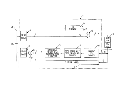
Fig. 1 is a schematic block diagram showing the overall
structure of an integrated circuit which constitutes a preferred
embodiment of the present invention;
Fig. 2 is an electrical schematic diagram showing the
major steps performed ~y the ECC Generator of the circuit of Fig.
l;
Fig. 3 is a flow chart of the decoding process performed
by the syndrome computer, the error locator NU(X) and error
evaluator (W(x) computer, and the factor NU(x), evaluate W(x), and
8a
C
~ 3 ~ 2 ~
69904-157
correction vector YI computer circuits of Fig. 1;
Fig. 4 is an electrical schematic diagram of the
Syndrome Compute circuit, part of the Syndrome Computer block 16
of the circuit of Fig. 1 and part of step 102 of the flowchart of
Fig. 3;
Fig. 5 is an elec~rical schematic diagram of par~ of the
Amend Syndrome Compute circuit, another part of the Syndrome
Computer block 16 of the circui~ of Fig. 1 and par~ of step 102 of
the flowchart of Fig. 3;
8b
.
~1 3 ~
6g904-157
Flg. 6 ls a flowchart of 'che computation of the error
locator polynomial NU(x), step 104 of Flg. 3 and part of the
Compute Error Locator Nu(x), Error ~valuator W(x) clrcult 18 of
Flg. l;
Flg. 7 is an electrlcal schematlc dlagram of the execu-
tlon of ~erlekamp~s algorithm as shown ln ~he flowchart o~ Flg. 6;
Flg. 8 ls an electrlcal schematlc dlagram of the remaln-
lng part of the executlon of Berlekamp~s algorlthm as shown in the
flowchart of Flg. 6;
Flg. 9 ls an electrical schematic dlagram of a Galois
Field comblnatlonal inverse calculator, which is clrcult 364 of
Fl~. 7~
Flg. 10 ls an electrlcal schematlc diagram of the cir-
cuit that computes the error evaluator polynomial W(x), namely
step 106 of Fig. 3;
Fig. 11 is an electrical schematic diagram of the clr-
cult that computes the value of the error locator polynomlal NUtX)
ln real tlme for each symbol of the code word, namely steps 108,
110, and 112 of Flg. 3;
~0 Fig. 12 is an electrical schematic diagram of the clr-
cult that computes the value of the error evaluator polynomial
W(x) ln real tlme for each symbol of the code word, namely step
114 of Flg. 3;
Flg. 13 is an electrlcal schematic diagram of the clr-
cult that computes the error locatlons and correctlon vectors of
code word symbols ln real tlme, comprlslng the circuits of Figs.
11 and 12, and also includlng steps 116, 118, and 120 of Fig. 3.
~X
: ~3~2~
69904-157
Fig. 14 ls an electrlcal schematic dlagram of the Galols
Field dlvide calculator, whlch is clrcult 524 of Flg. 13;
Flg. 15 ls a timing diagram showlng the tlme allocat lons
for calculatlons and data transfers ln the clrcult of the present
lnvention;
Flg. 16 ls an electrlcal schematlc dlagram of an .XOR.
network that functlons as a GF a~33 multlplier;
Fig. 17 ls an electrical schematlc diagram of an .XOR.
network that functlons as a GF a~32 multlpller;
Flg. 18 ls an electrlcal schematlc dlagram of an .XOR.
network known as a Shlft-l clrcult that performs the functlon of a
GF al multiplier;
Flg. l9 ls an electrlcal schematlc dlagram of an .XOR.
network known as a Shift-2 clrcult that performs the functlon of a
GF a multlpller~
Flg. 20A ls an electrlcal schematlc dlagram of a circult
to compute [SYMBOL A] x a~33 and lSYMBOL A] x a~32 uslng the a~33
multiplier of Fig. 16 and the al multipller of Fig. 18;
Flg. 20B ls an electrlcal schematic dia~ram of a circuit
to compute [SYMBOL B] x a30 and [SYMBOL B] x a32 using an a30
multiplier and the Shift-2 circult of Flg. 19~
Fig. 21 is an electrlcal schematlc dlagram of a prefer-
red embodlment of the Syndrome Compute clrcult of Flg. 4 uslng the
Shlft-l clrcult of Flg. 18 to ellmlnate approxlmately half of the
multlpller circultry;
~ , .
-- ~31~
69904-157
Flg. 22A ls a second pre~erred embodiment of the NUeVen
circuit of Flg. 13 using the Shlf~-2 clrcult o~ Fig. 19;
Flg. 22~ is an electrical schematic ~lagram of a second
preferred embodlment of the Nuodd clrcult of Fig. 13 using the
Shift-2 circult of Flg. 19;
Fig. 23 ls an electrlcal schematlc diagram of a second
preferred embodiment of the error evaluator polynomial W(x) compu-
ter of Flg. 12 uslng the Shlft-l clrcult of Elg. 18;
DESCRIPTION OF THE PREEERRED EMBODIMENT
Reference will now be made in detail to the present
preferred embodiment of the lnven~ion as lllustrated ln the
accompanylng drawlngs.
The present preferred embodlment of the Reed-Solomon
error detectlng and correctlng clrcuit is shown ln block diagram
form ln Flgure 1 and ls represented generally by the numeral 10.
As embodled herein, clrcuit 10 accepts binary data from data bus
28 of a data processing system (not shown) and converts those data
blts lnto K m-blt data symbols, dl, where i = 1 to K. Data
symbols di are simultaneously sent to an Error Correction Code
~0 (ECC) generator 14 and a data storage dlsk 26 through a
multiplexer 15.
In accordance wlth the lnventlon, there ls provlded
encoder means for encodlng the data symbols lnto a plurallty of
Reed-Solomon flrst code words a(x) and sendlng the flrst code
words to the error lnducing medlum. As embodied herein, ECC
generator 14 generates N-K ECC s~mbols el, where 1 = 0 to N-K-l,
using a generator polynomlal g(x) havlng roots ai, -34 ~ i ~ 34,
~31~2~
69904-157
where a is a prlmltlve element of the Galols Field GF ( 2m ) . N
represents the length of the code word and is an ln~eger ~2m. The
N-K ECC symbols el are appended by multiplexer 15 to the K data
symbols dl to create an N symbol Reed-Solomon (N,K) code word
a(x), conslstlng of N symbols al, which is stored on data storage
disk 26. A header fleld ls also provlded for each code word whlch
provldes separatlon between code words, and other storage func-
tlons, and ls not described in detall. Storage devlce 26 ls an
example which contalns an error induclng medium where errors can
be created as data are being stored and retrieved.
Errors may occur to the symbols of code word a(x) when
stored on and retrieved from storage device 26. When read from
the dlsk, code word a(x) ls deslgnated y(x) because lt may contaln
erroneous symbols. Where there are no errors present, ~(x) equals
a(x), or equivalently p(x) = 0.
In accordance with the invention, there is provlded
buffer means for receiving from the error lnducing medium a plur-
ality of retrieved code words y(x) equal to the first code words
ln which errors have been induced and for holding each of the
retrieved code words long enough to compute error locations and
values, preferably for no longer than the time needed to compute
error locations and values. As embodied herein, data symbols read
from data storage disk 26 are held in a data buffer 22. The
invention further includes decoder means for computing from the
retrieved code words a plurallty of error locatlons and correctlon
12
~;
6ggO4-157
vectors ln real tlme as each symbol of the retrieved code word
exlts from the buffer means. As hereln embodied, the ~ecodlng
means, lncludlng a Syndrome Computer 16, an Error Locator and an
Error Evaluator Computer 18, and an Error Correction Vec~or
Computer 20, calculates the error location and correctlon vector
for data symbols belng held in buffer 22.
As hereln embodied, Syndrome Computer 16 beglns calcu-
lating syndromes as the code word symbols are read from data
storage device 26. Error locator and error evaluator computer 18
computes the error locator polynomial NU(x~ by solvlng the
Berlekamp-Massey algorithm uslng syndromes computed ln Syndrome
Computer 16. The terms of error evaluator polynomial W(x) are
also calculated ln computer 18 uslng the values of NU(x) and
syndromes from Syndrome Computer 16.
In accordance with the inventlon, there is provlded
correcting means responsive to the error locatlons and correctlon
vectors for correcting erroneous data symbols as they exit the
buffer means. As herein embodled, as each data symbol d'i ls
released from buffer 22, computer 20 calculates error locator
polynomlal NU(x) uslng a modl~led Chlen search algorlthm, and
evaluates error evaluator polynomlal W(x) to compute a correctlon
vector YI that is exclusive or'd by .X0~. clrcuit 24 with the d~ta
symbol belng released from buffer 22. Data symbols of the decoded
code word are converted lnto 16 bit data words by converter 27 and
are returned to the data processing device 16 blt data bus 28.
~3~2~
6ggO~-157
The "pipe-lining~ or hlgh speed compu~atlon o~ error
values and locatlons ln real tlme as data are released from buffer
22 ls a ma~or ~actor in achievlng the low latency, or low holdup
time, which permits the clrcult of the present lnventlon to
achleve a hlgh bandwidth.
Uslng VLSI loglc to execute a Reed-Solomon error cor-
rectlng function, the circuit o~ the preferred embodlment achieves
an acceptably low error rate for decode~ data ~rom sectorlzed data
storage devlces such as magnetlc dlsks, magnetlc tapes, and optl-
cal dlsks havlng hlgh inherent error rates. The clrcult provldes
a high bandwldth of approxlmately 70 megablts per second and a low
latency of about 144 microseconds at peak bandwldth uslng a stan-
dard dlsk sector slze of 480 symbols where up to 32 ten blt sym-
bols may need to be corrected, requlrlng an overhead of 670 ECC
blts. This permits operatlon of storage devlces at a net data
denslty higher than certain earller data storage systems.
Preferably, and as shown ln Fig, 1, blnary data blts
destlned for storage on magnetlc dlsk 26 are recelved from a data
processlng system (not shown) vla a 16 blt data bus 28. The
~0 binary data, which consist of both lnformatlon words, and Error
Detecting Code (EDC) words are converted ln converter 12 to a
serles of K symbols, where each symbol ls m-bits long. In the
preferred embodlment, each symbol ls 10 bits long, and K is
selectable from 48 to 941 data symbols. The 10 blt symbols are
assembled from data words and EDC words, each word belng 16 bits
long. The 16 blt words are converted to symbols untll all data
14
~ 3 ~
69904-157
words and EDC words have been converte~ ~o ten blt ~ata symbols,
represented by di. ~nough ~111 blts are added to provlde complete
symbols. Data symbols dl are sent both to storage dlsk 26 and ECC
generator 14.
As here embodled, the encoder means lncludes ECC genera
tor 14. ECC symbols el which wlll be used to detect and correct
errors in the data symbols di are computed by ECC generator 14
using a generator polynomlal g(x). The error correction code
chosen is a symmetrlc Reed-Solomon code over the Galois Fleld
GF(210) generated by the prlmltlve polynomlal x10 ~ ~3 + 1. For
the Reed-Solomon code of the preferred embodlment, the generator
polynomial, g(xl is defined as:
Equatlon 1
+33
g(X) ~ al)
1--33
where al are elements of GF(210). GF(210l contains 1023 elements,
therefore a code word of N = 1023 symbols can be generated. Code
words ln the preferred embodlment are llmlted to N = 115 to 1008
symbols by the deslgn of lntegrated clrcult 10 of Flg. 1. The
generator polynomial g(x) is chosen to generate 67 ECC symbols,
therefore N-K is 67 whlch suffices to correct up to 32 symbols ln
error per sector or code word, provide a 100~ probability of
detectlng all errors up to 35 errors per sector, and provlde a
strong llkellhood of detectln~ all errors greater than 35 per
sector. The polynomlal g~x) ls so deflned that when expanded lnto
lts lndivldual terms, it has symmetrlc coefficients
:. :
.
69904-157
so that the Galois Field multiplier circuits, defined
mathematically below, can he reduced by a ~actor of 2, that is,
each a term appears twice in g(x) as a coefficien~ of a different
power of x. Equatlons 2 and 3 are expanslons of Equation 1.
Equation 3 shows the individual terms of g(x).
Eq~ation 2
g(x) = ~ + a 33)(x + a~32) 33
Equation 3
67 3sx66 + al46X65 + a572x6~ + a47x ~ a x -~
10a950x611 a820x60 ~ Cy3l2x59 ~ C~177X58 + a259X57 + a530X56 ~
444 5S974xS4 + a349x53 ~ a255x52 + a26 x + a x +
a x + a 96X48 + a636X47 + a715x46 + 475 45 247 44
957 43 63X42 + a37x41 + a573x40 + a69 x ~ ~ ~ +
a733x37 + al38x36 + ~41X35 + a552X34 + a552X33 + a41X32 +
a x + a 88X30 + a598x29 ~ a691X28 + 673 27 37 26
a x + a 57x24 ~ a247X23 + a475X22 ~ a715X21 636 20
a x + a 4X18 1 a898x17 ~ a261x16 + ~55 15 349 14
a x + a 44X12 + a530x11 + a259X10 ~ 177 9 812 8
a x ~ a x + a505x5 + a47x4 + a572x3 + 146 2 35
~0 Fig. 2 shows the circuit used by ECC generator 14 to
generate the 67 ECC symbols ei by dividing d(x)*xN K by g(x),
where d(x) is a polynomial of degree K-1 with coefficients equal
to di. Mathematically, the code word a(x) is a polynomial with
coefficients ai and consists of the 67 ECC symbols ei appended to
the data symbols, di. Note that in the examples which follow,
exactly 4413 data symbols are chosen. Syndrome modifiers
referenced later are based on thls choice of 413 data symbols. If
16
~ 3 ~
~ 9904-157
a(x) is considered to be a N-1 degree polynomial in x wlth the
symbols ai as coefficients, then
Equation 4
a(x) = aN 1xN 1 + aN_2xN 2 ~ a1x~a0
The coafficients of the ~irst K ~erms are di, and the coefficients
of the last ~ K or 67 ~erms o~ the polynomial are ei. The ECC
symbols are generated by dividing d(x) * xN K by g(x), as shown by
the circuit of Fig. 2, which amounts to dividing the incoming data
stream di by g(x). Circuit 1~ in~ludes 67 shift registers,
labeled E(O), E~l), ... Et66), each of which is pre~erably a 10
bit parallel shift register, with the number in parentheses being
the power of x represented by that register. The data s~ream of
413 data symbols is read into ECC generator 14 as the data symbols
are being sent to disk 26 for storage. The mode of generator 14
is then switched by blocking both the data gate 42 and the
feedback gate 44 to txansfer ECC symbols out of circuit 14 to be
appended to the data symbols. Blocking the feedback gate also
clears the ECC genexator for the next sector's data. The +
symbols, one of which ls labeled 46 in Fig. 2, indicate a parallel
.XOR. or modulo-2 add ~unction. The x ai symbols, one of which is
labeled 48, indicate a Galoiæ Field multiply by ai, which is
equivalent to raising the exponent of an input symbol by i, for
example ai *ai ~
~3~2~
69904-157
ai~ where 1+~ ls computed modulo 1023. All GF multlply
operations are modulo the prlmltlve polynomlal x10 + x3 ~ 1.
Multlpllcatlon on the Galols Field ls deflned as follows
If p and q are any two 10 blt symbols where each bit ls pO, pl,
... p9 and qO, ql, ... q9, then the GF multlply functlon ls
deflned as:
Equatlon 5
p x ~ [(p9x9 -~ p9x8 .. pOxO)(q9x9 + p9x8 qOO)]
modulv x10 ~ x3 + 1
-x91p9(qO + ~7) + p8(ql ~ q8) + p7(q2 ~ q9)
~ p6q3 + p5q4 + p4~5 + p3q6 + p2~7 ~ plq8 + pOq9] +
x8~p9(~6 + q9) + p8(qO q7) + p7(ql + ~8) + p6(q2 + q9)
+ p5~3 + p4q4 + p3~5 + p2q6 + plq7 + pOq8] +
x7~ . . .
The coefficlents of the remalnlng terms (x7 to x) are the normal
products of the polynomlals, modulo x10 + ~3 + 1. Because the
elements of p and q are blnary dlglts, coefflclents of the form
pl(q~+qk) are equlvalent to Pl .AND. (q~ .XOR. qk) and may be
calculated ln hardware ln the normal manner. Any product ls an
.AND. and any addltlon ln parentheses ls a modulo-2 addltlon, or
.XOR.
Because the Reed-Solomon code ls cycllc, a 67 symbol
"coset leader" ls .XOR.'d wlth the 67 ECC symbols as they are
shlfted out of clrcult 14. The coset leader prevents the decodlng
portlon of clrcult 10 from mlsinterpretlng and acceptlng a sector
that has lmproperly been shlfted. A shlft of blts that have been
18
.
~ 3 l ~
69904-157
.XOR.'d With the coset leader causes clrcult 10 to lnterpret all
data ln that sector as containlng ~2 errors. During the data
read operatlon, discussed hereinbelow, the 67 ECC symhols as read
from th~ disk sector are agaln .XOR.'d wlth the same coset leader
symbols, removlng them from ~he ECC symbols and havlng no effect
on further calculations unless the symbols were shifted, and then
excessive errors will be generated ln accordance wlth the normal
functioning of the decodlng clrcult.
The coset leader ls .XOR.'d to the ~CC symbols ln the
normal manner. The 67 coset leader symbols of the present
inventlon are selected from a code word of a Reed-Solomon code
that contains the Reed-Solomon code of the present inventlon as a
subset. As determlned by experimentation, the code word from
whlch the coset leader is selected must have no more than 67 non-
zero symbols. There is no known method for ~electing an optimum
coset leader, but the coset leader of the preferred embodiment,
shown in Table 1, wlll result ln 33 or more errors if the symbols
of the code word are shlfted by up to 100 blts. Startlng wlth the
last symbol, the coset leader symbols ln octal are:
~ , .
'',''~",
.. . . .
~ 3 ~
69904-157
TABLE 1
Symbol No. Value Symbol Value Symbol Value
0 404 23 324 46 1125
l 1245 24 1722 47 1~01
2 1026 25 1413 48 402
3 722 26 100~ 49 1564
4 1347 27 777 50 1604
1147 28 1370 51 627
245 2g 1526 52 776
7 1140 30 471 53 1275
8 457 31 162~ 54 135
9 560 32 573 55 5~1
164 33 402 56 42
11 1~07 34 1562 57 410
12 1647 35 743 58 1632
13 362 36 421 5~ 1313
14 326 37 1230 60 1223
401 38 55 61 531
16 567 39 1453 62 1745
17 314 40 233 63 1442
18 1532 41 257 64 777
19 1142 42 665 65 1632
707 43 1525 66 630
21 424 44 1415
22 665 45 1301
After a varylng amount of data storage time determlned
by the dlsk user, code word y(x) ls read from dlsk 26. Because of
posslble errors ln code word symbols, a~x) is now represented by
y(x). If there are no errors ln y(x), then a(x) = y~x). The flow
chart of Flg. 3 shows the sequence of events performed by the
decoder portlon of clrcuit 10 whlch lncludes syndrome generating
means, step 102; the means for calculatlng error locator
polynomial NU~x), step 104, and èrror evaluator polynomlal W(x),
step 106; and means for slmultaneously calculatlng the value of
the error locator polynomlal NU(x), steps 108, 110, and 112, and
the value of the error evaluator polynomlal W(x), step 114, and
means for correctlng erroneous symbols ln code word y(x)
.. : ,.,,, . ~ ,.. ~....................... -
~3~0~
699~4-157
to ~rror free symbols al ln rsal time as each root of NU(x) and
value of W(x~ ls calculated, steps 116, 118, 120 and 122. On Fig.
3, N represents the code length ln symbols and I represents the
symbol number.
Syndrome computer 16 of Fig. 1 generates syndromes Sl,
step 102 of Flg. 3, whlch are the coefflclents of a polynomlal
S(x). Flg. 4 shows the clrcult used to compute S(x)
slmultaneously as the symbols of code word y(x) are read from a
sector of disk 26. The calculatlon belng performed by the circult
of Flg. 4 is:
E~uatlon 6
N-l
S~ = ~ Yl x a 1~ for -34 c ~ c 34
1=0
The calculatlon ls performed by a Galols Fleld multlplier means
conslstlng of an array of 10 blt wide reglsters, labeled S33 to
S_33, GF multlpliers, adders, and .AND. gates, each of whlch is an
S computer. As in Flg. 2 xal symbols indicate a GF multiply
operation, and ~ symbols lndicate a modulo-2 addition, or .XOR. A
mode swltch occurs by deasserting feedback gate 150 after 479
symbols have been transferred into all 67 S computers, at which
point all 67 .AND. gates, one of which is identlfied as 152, are
blocked and the 480th symbol is simultaneously entered into the 67
S computers. Blocklng feedback gate 150 clears all S computers in
preparatlon for calculating syndrome~ for the next sector.
.
,
.
- ~L310~2~
69904-157
In a second preferred embodiment a substantial reductlon
ln hardware was achieved by maklng the Galols Fiel~ multlpller
means of the syndrome computer o~ ~lg. 4 operate on a hal~ sym~ol
clock l70 ns.) even though lt accepts lnput symbols at half that
rate. This allows a hardware savlngs because each multlpller can
be used twlce ln a full symbol perlod to generate two partlal
syndromes, therefore only 34 o~ the 67 alpha multlpliers need be
built. Each ad~acent multlpller i8 related by a slmple functlon.
As an example, a~32 can be derlved by taking a~33 and multlplylng
lt by al (-33 ~ 1 = -32). Multlplying by al ls equlvalent to
shifting once and XORlng blt 9 wlth blt 2.
Glven a 10 blt symbol 9 8 7 6 5 4 3 2 1 O, this symbol
multlplied by al would become 8 7 6 5 4 3 9.XOR.2 1 0 9. This ls
a much slmpler and smaller function to build than an a~32 multl-
pller. All even numbered alpha multlpliers in the syndrome compu-
ter are derived from the odd numbered alpha multlpllers ln thls
manner. Thls same hardware reductlon technlque ls also used ln
the YI computer 20 of Flg. 1, and wlll be dlscussed in greater
detail herelnbelow.
The 67 syndrome values Sl are next passed to the S'(K)
reglsters of amend syndrome clrcult 200 of Flg. 5. Except for
syndrome value S33, syndrome values are lnput through multi-
plexers, one of whlch ls identifled by the numeral 204. Thls
releases the S calculator circuit of Flg. 4 to calculate syndromes
for the next code word to be read. Clrcuit 200 ls also part of
syndrome generator 16 of Fig. 1. The amend syndrome functlon
'' ' .''~
~ 3 ~
6990~-157
shortens the code symbols of GF(2l0) from a maximum of 1023
symbols to the 480 symbols used ln the example and stores the
amend syndromes for the shortened code ln the SY reglsters, 210 of
Fig. 5. Amend syndrome computation starts wlth a ~roadside load
of the 67 syndromes, S(K), lnto S'(K) reglsters, labeled S'(-33)
to S'(3~). Slmultaneously, register 202 is cleared and loade~
wlth the value of a462~ whlch ls equal to 0001010101. Multl-
plexers connected to S'(K) reglsters lsolate the S~K) lnput and
connect each S'(K) register to the next hlgher S'(K-l) register.
The flrst multlpllcatlon to take place ln GF multlpller 206 ls
S(-33) x a462 which ls then shifted lnto shlft reglster SY(0).
Multlplexer 208 lsolates the a462 slgnal from reglster 202 and
allgns the GF x a544 multlplier so that when syndrome S(-32) ls
shifted lnto reglster S'(-33) it wlll be multlplled by the con-
tents of reglster 202 whlch is the GF product of a462 and a544.
Each amend syndrome ln reglster SY(K) ls therefore the GF product
of the syndrome value from the S'(K) reglster multlplled by
(a462)(a544)n~l. The x a544 functlon ls the same GF multlpll
catlon deflned by Equatlon 5, but may be lmplemented by the
followlng .XOR. operations, where l are the output bits of a 10
blt symbol, and Il are the lnput blts.
Table 2
g Io ~ I2 ~ I3 ~ Is ~ I6
8 = Io ~ I2 ~ I4 ~ I5
o7 = Io ~ 3 ~ I4 ~ I~
6 = Io ~ I2 ~ I3 ~ I8
23
~ .
~31~2~
69904-1~7
o5 = Il ~ I2 ~ I7
4 = Io ~ I6
O3 = Io ~ I5 ~ Ig
2 = Io ~ I2 ~ I3 ~ I4 ~ Is ~ I6 ~ Ig
l = Io ~ I2 ~ I3 ~ I4 ~ I5 ~ I7 ~ I8
oO = Io ~ I2 ~ I3 ~ I4 ~ I6 ~ I7
The 462 and a544 multlpllers of circuit 200 are pro-
grammable in the circuit of the preferred embodlment and must be
changed lf the code word length is altered from 480 symbols.
The means for generatlng the NU~x) error locator poly-
nomlal ls shown ln Fig. 1 as clrcult 18. Amend syndromes, SY(K)
are now used to compute NU(x) uslng the Berlekamp-Ma sey algor-
lthm, as modified by Weng, and uslng a data flow technlque as
suggested by Rlggle to lncrease processing speed, step 104 of Fig.
3, and shown more completely as the flow chart of Flg. 6.
The flow chart of Flg. 6 shows the lndivldual steps
performed during the calculatlon of NU(x). Fig. 6 is broken down
lnto sectlons by clock cycles or states, described in more detail
herelnbelow, to show operations performed simultaneously. For the
sake of clarity, quantitles calculated in one sectlon of the chart
are made avallable to other boxes ln the chart, but connecting
lines are not shown.
The lnitial condltions for Fig. 6 are shown ln step 252.
The quantlty D in step 252 ls the lnteger value of the code dis-
tance, N - K ~ 1 = 68. The ~uantlty Y, calculated in Step 260, is
de~lned to be 0 when DU~0. A state machine ~not shown)
24
-- !1 3~0~21
69904-157
controls the process steps whlch are repeated 67 kimes. Referrlng
also to Fig. 7, during state 1, multlplexers (not shown) connect
32 symbol wide GF multipller 350 to 32 SY reglsters 210 (SY(l)-
.SY(32~) and 32 NU reglsters 352. The GF product ls performed as
deflned by Equatlon 5 on the NU and SY reglsters. Thls completes
step 254 of Flg. 6. The product, X(I) of Flg. 6, ls shlfted to
not-shift reglsters (not shown), and ls excluslve OR'd ln tree
fashlon wlth SY(O) by the +T function 354 o~ Flg. 7 untll a slngle
lO bit symbol, DU, appears on 10 blt bus 356. Thls completes step
256 of Fig. 6. The +T functlon is the concatenated .XOR. sum of
all inputs. If there are n inputs I~, then the output O = Io ~ I
. . . ~ In~ For maxlmum speed the .XOR.'s are treed as shown
below.
Table 3
Io Il I2 I3 I4 I5 I6 I7 . . .
\ / \/ \l \l
+ + + +
\ / \ / :
\. . . . . . . /
During state 1, the single 10 blt symbol ls clocked lnto
DU reglsters 358 and ls clocked to the output stage of reglsters
358 during state 2. Simultaneously, as shown ln step 258 of Fig.
6, the counting reglster 360 of Flg. 7 contalning counter variable
LLMR ls decremented by 1 and tested for a condltlon of belng less
. ~,
~3~2~
69904-157
than 0. I~ less than 0, gate 362 is enabled. As shown ln step
260 of Fig. 6, during state 2 the value of DU ln shlft reglster
358 of Fig. 7 ls shlfte~ to the oUtpUt and is used to (1) compute
a neW value of Y by an inverslon process 364 of Flg. 7, descrlbed
hereinbelow, (2) compute a new value of Q = DU x P, step 262 of
Fig. 6 per~ormed by GF multipller 366 of Flg. 7, and (3) test for
DU = 0, loglc test 368 of Flg. 7 and step 264 of Fig. 6. If DU =
0 and LLMR cO then EN is set as a flag vla gate 362. Inverslon
operation 364 i9 performed accordlng to a procedure developed by
Lih-Jyh Weng, and is shown in Flg. 8.
The GF lnverse clrcult 364 of Fig. 7 ls shown ln more
detail in Fig. 9. The clrcult of Fig. 9 computes the inverse a~n
of an lnput symbol an by ralslng the input symbol to the 32 power
and multlplylng lt by the input symbol lowered to the -33 power.
The result of a32n xa~33n ls a~n. To accomplish thls a 10 bit
symbol an ls lnput to an a32 .XOR. network 400, wlth blt lnputs I
and blt outputs i as shown below.
Table_4
og = I2 ~ I3 ~ I4 ~ Ig
8 Il ~ I2 ~ Is ~ I6 ~ I7 ~ I8 ~ Ig
07 = I7
6 = I2 ~ I3 ~ I5
5 = Il ~ I3 w I4 ~ I6 ~ I7 ~ Ig
04 = Il ~ I2 ~ I7 ~ Ig
m m m
03 = I2 ~ I6 ~ I7 ~ I8 ~ Ig
2 = Il ~ I2 ~ I3 ~ I4 ~ I6 mw I8
26
4 ~ 1
69~04-1~7
l = Il ~ I4 ~ I6 ~ I7 ~ I8 ~ I9
o = Io ~ I2 ~ I3 ~ 4 ~ I7
Each ~ represents an .XOR. The value a32n ls mul~iplled by an to
get a33n. Because a33n are elemen~s o~ a subfl~ld, GF(25), of
GF(210), there are only 31 possible non-zero values for any a33n.
Using a selected S of the 10 bits available (Io,I~ , I3, I5),
it is posslble to construct a loglc network ~s ~efined by Table 5
below whlch output~ the 31 lnverses o~ a33n (i.e., all a~33n). i
are the output bits o~ the a~33n network that are computed from
the lnput bits Il. The input blts are the 10 blts of the symbol
a33n and the output blts are the 10 blts of the symbol a~33n.
Table 5
09 = Zl+Zs+z6+z7+zs+zzo+zzl+zz2+zz3
+Zl6+zls+z20+ 25+ 27+ 28+ 30
8 = Z3+Z5+Z6+Z8+zlo+zl4+zls+zl6+zl8
+Zl9+Z20+Z21+Z22+Z25+Z28+Z29
7 =
6 = Z4+z6+z7+z9+zll+Zl5+zl6+zl7+zl9
+Z20+Z21+Z22+Z23+Z2~+Z29+z3
5 = Zl+z3+z7+z8+zg+zll+zl2+zl3+zz4
+Z15+Zl8+z2l+z22+z27+z29+ 30
4 = Zl+Z3+Z4+Z6+Z8+1z2+Z13+Z14+Z16
+Zl7+zl8+zlg+ 20+Z23+z26+z27
3 = Z2+Z5+Z6+Zll+Z13+Z14+Z16+Z18+Z22
+Z23+z24+~26+z27+z28+z29+z30
2 8 Zl+Z2+Z3+Z4+Z5+Z8+Zll+Zlz2+Z17
+Zl9+Z20+Z22+Z24+Z28+ 2g+Z30
l = Zl+Z2+Z7+zs+zlo+zl2+zl4+zls+zls
+Z20+z22+z23+z24+z25+z26+z29
o = Zo+Zl+Z3+zs+zs+zlo+zll~zl3+zl4
~'
.
.
~3~2~
69g04-157
+ZlS+Z16~Z17+Z20~ZZ3~Z24+Z29
Z0=I0IlI2I3I5 Zl=IoIlI2I3Is Z2~IoIlI2I3I5 Z3 IoIlI2I3 5
Z4 I0IlI2I3I5 Z5 IoIII2I3Is Z6 IoIlI2I3I5 Z7 IoIlI~I3I5
Z8=IoIlI2I3I5 Z9=IoIlI2I3I5 Zlo=-loIlI2I3I5 Zll I0I1~2~3 5
12 I0IlI2I3I5 Zl3=IoIlI~I3Is zl4=IoIlI2I3I5 Z15=I0IlI~I3I5
Zl6=IoIlI2I8Is Z17 IoIlI2I3Is Zlg-IoIlI2I3I5 Zlg=IoIlI2I3I5
Z20 I0IlI2I3I5 Z21=I0IlI2I3I5 Z22=I0IlI2I3I5 ~23=IoIlI2I3I5
224=IOIlI2I3I5 Z25=IOIlI2I3I5 Z26=IOIlI2I3I5 Z27=IoIlI2I3I5
Z28=IoIlI2I3I5 Z29=~IoIlI2I3I5 Z3o=IoIlI~I3I5
The flnal operatlon to lnvert an ls to multlply ~32n by a~33n to
yleld a-n accordlng to equatlon 5, presented earller.
If EN is set, durlng state 3 LLMR has lts slgn blt
complemented, step 268 of Fig. 6, NR lnput contents are replaced
by NU contents, step 270, and the value of P ls replaced by the
value of Y. If EN ls not set, then NR ls shifted upwards (towards
higher order terms). Also durlng state 3, NU input contents are
replaced wlth the NU outputs .XOR.'d wlth NR ~ Q, step 274 of Flg.
6, and SY reglsters are shlfted upwards, step 266. When thls has
been completed, one of 67 loops has been completed as counted by R
ln step 276 of Fl~. 6. Durlng the 67th loop, the SY reglster
shlft ls omltted to prepare for the W(x) computatlon. A test of
LLMR ls made durlng each loop to assure that LLMR ls <0. If it ls
not, then there are more than 32 = T errors ln the code word and
the sector ls not correctable. After all 67 steps have been
performed, the flnal NU(I) are coefflclents of the error locator
polynomlal NU(~) for 0 c I c (T~l), and NU(0)=1.
28
~;
~` ~3~0~21
69904-157
Circuit 448 of Flg. 10 lncludes means for calculating
error evaluator polynomlal W(x). As embodied hereln, the means
for computing the values o~ error evaluator polynomial W(x)
comprlses w reglsters 450, amend syndrome 54 reglsters 210, error
locator polynomlal NV registers 352, multlplier 350, and treed
adder 354 whlch executes the procedure shown in Flg. 3, includin~,
speciflcally step 10~. For simpliclty, the calculatlon ls shown
in step 106 ln an inverse form. The coefficlents of W'(x) are the
coefflclents of W(x) only ln reversed order. To lllustrate:
Equatlon 7
If
p(X) = po + plX + p2X ~ ...pkX
then
p (x) = Pk + Pk_lX + Pk-2X2 + ,,,poXk
The same is true for S'(x) and NU'(x). The mode of the NU(x)
computer changes to a W(x) computer mode, shown ln Flg. 10.
Multlplexers (not shown) are set to connect NU reglsters 352 and
SY reglsters 210 to GF multlpller 350 and tree'd .XOR. functlon
354 throughout computatlon of W(x). Ten blt bus 356 ls connected
to register W(31) of W(I) shift registers 450.
Startlng wlth a new state 1, the products of SY and NU
are multiplied by GF multlplier 350 and are tree .XOR.'d by devlce
354, the operatlon of whlch have both been descrlbed herelnabove.
A slngle 10 blt symbol ls lnput to reglster W(31) from bus 356.
Durlng state 2, the contents of all W(I) reglsters are lnput to
all W(I-l) reglsters viq 32 ten blt symbol busses 452
~3~2~
69gO4-157
(~ownshiftlng $he W values) and all SY(I) values are shlf~ed to
SY(I~l) (upshlfting the SY(I) values). S~ates 1 and 2 are
repeated untll 32 cycles have been completed. The contents of
W(I) reglsters 450 contaln the coefflc~ents of error evaluator
polynomlal W(x~ ànd the NU(I) reglsters 352 contaln the coeffi-
clents of the error locator polynomlal NU(x). NU(I) and W(I)
values are then transferred ~o the next functions, steps 108, 110,
112, and 114 of Fig. 3. Reglsters 210, 352, and 450 are cleared
in preparation for computing NU(x) and W(x) for the next code
10 word.
The circults of Fig. 13 provlde the means for slmul-
taneously solvlng the error locator polynomial NU(x~, ~or obtaln-
lng the correspondlng error value from NU(x) and W(x), and for
correctlng erroneous symbols in code word y(x) to error free
symbols al as each symbol ls shlfted out of buffer 22 of Flg. 1,
which lncludes the steps of (1) solving each term of NU(x),
summlng the odd and even power terms into NUodd(x) and NUeven(x)
respectlvely, step 108 of Flg. 3, (2) slmultaneously evaluatlng
W(x), and (3) correctlng errors in y(x) as indicated by the error
locatlons and error values derlved from the calculated values of
NUodd(x) and W(x). In order to generate a correctlon symbol, or
correctlon vector YI, whlch is a non-zero coefficlent of p(x) for
a glven code word symbol, the error value computatlon clrcult 20
of Fig. 1 evaluates the 32 symbol values of NU(x) plus the lowest
order coefflclent of NU(x) which ls always 1, and the 32 symbol
values of W(x) for each code word symbol wlthin the sector in real
~3~0421
6g904-157
tlme at the same tlme as the correspondlng symbol is shifted out
of bu~fer 22 of Flg. 1. The results of thege evaluations are then
manipulated to generate the actual correction polynomial p(x).
To determine error locations, the usual practice ls to
use a Chlen search, where all posslble legltlmate values of x are
tested to flnd the roots of NU(x). ~ased on those roots, the
erroneous symbols are identified, W(x) evaluated, and y(x) la~er
corrected. However, the standard techni~ue requlres more latency
than the present inventlon. To provide the advantage of low
latency, the Chien search ls modlfied to permit slmultaneous
evaluation of W(x), data flow is pipelined, and erroneous symbols
are identi~led and corrected in real time as they exit buffer 22
of Fig. l on their way to data processing bus ~8. Thls requires a
Chien search as modifled by the present inVention to compute the
value of NU(x) and W(x) as each symbol exits buf~er 22, whereupon
a decislon i5 made as to whether the symbol ls lncorrect. If
lncorrect, the non-zero coefflcient ln p(x), computed from NU(x)
and W(x), amends the erroneous symbol in .XOR. circuit 2~.
Clrcuit 480 of Flg. 11, consisting of a plurality of
Galols Fleld multipller means, each containing a 10 bit shift
reglster and a Galois Fleld multlpller network, e~aluates NU(a~)
as each code symbol ls tlmed to exlt buffer 22 of Flg. 1, where i
is the number of the symbol exltlng buffer 22 of Fig. 1. During
each clock cycle, the contents of each NU reglster NUl to NU32 ls
multlplled by the GF multlpller connected to the register, thereby
31
~ 3 1 ~
6~904-157
testing for a root ~1 0~ NU for each clock cycle. The contents of
each NU register o~ circuit 480 ls multlplled by its correspondin~
GF multlpller once for each corresponding data symbol. Values of
NU for the even powers of x and values of NU for the odd powers of
x are summed separately and are referred to as NUeVen and NUod~
Thls completes steps 110 and 112 of Flg. 3. NUodd ls requlred for
subsequent error value calculations. At the same time as the
NU(x) calculatlons, W(x) is also being evaluated ~y clrcult 500 of
Flg. 12 once for each symbol exlting buffer 22. In particular,
clrcuit 500 of Fig. 12 computes W(ai) x a34i for each symbol, cor-
respondlng to step 116 of Flg. 3.
Looking to Fig. 13, circuit 480 i5 the same circuit as
shown ln Flg. 11, and clrcult 500 ls the same circuit as shown in
Fig. 12. Summer 520 computes NU(x) as the sum of NUodd and
NUeVen. If NU(x) = 1 then the 1th symbol of the code word exitlng
buffer 22 is in error, and gate 522 enables one input of gates 528
and 530, corresponding to step 120 of Fig. 3. At the same tlme,
and regardless of whether the 1th symbol is correct or not, dlvi-
der clrcuit 524 computes the correct value, or correction vector
2Q of the ith code word symbol. This is shown as YI ln step 116 of
Flg. 3 and will be discussed in more detail hereinbelow. Also at
the same time, loglc gate 526 checks for NUodd = 0. If lt ls zero
and NUeVen = 1, then gate 528 sets a system flag indlcatlng to
data procéssing system 28 of ~lg. 1 that the decoded output of
circuit 10 is erroneous. The dlsposltion of the erroneous data is
left up to the data processing system. Also, lf NUodd = 0,
~L 3 1 ~
6g904~157
correction vector YI wlll not be gated to .XOR. circult 24 ~ecause
gate 530 of Fig. 13 will be locked open. This corresponds to step
118 of Fig. 3. An error locatlon foun~ whlle NUodd = 0 lndlcates
a malfunctlon of tha decoding process.
Dlvlder clrcult 52~ o~ Flg. 13, shown ln greater detall
ln Flg. 14, operates ln a similar manner to the GF lnverse clrcult
of Fig. 9 except that a second input and thlrd multlpller have
been added. Dlvlder 524 calculates the correctlon vector YI, step
116 of Flg. 3, by dlvldlng Z from step 114, whlch is represented
by symbol am of Flg. 14, by NUodd~ whlch is represented by symbol
an of Fig. 14. The resultlng correctlon vector ls therefore:
E~uatlon 8
YI = W(al)(a34l)
NUodd (~
This completes step 116 of Flg. 3.
Clrcult 24 of Flg. 1 amends erroneous code word symbols
by .XOR.lng the data stream from buffer 22 wlth the correctlon
vectors, step 122 of Flg. 3. When a symbol ls not ln error, gate
530 of Flg. 13 is open and the correction vector ls zero, there-
fore .XOR. clrcult 24 leaves the data symbol unchanged. The
bu~fer data stream must be synchronlzed wlth the computatlon of
error values so that the correctlon vectors match the correct data
~mbols~
Buffer clrcuit 22 of Flg. 1 ls a large flrst-ln-flrst-
out storage unlt for data read from disk data port 25 and provides
33
,
~ 3 ~
6990~-157
data to the dat~ amend clrcuit 24 app~oxlmately 2 sec~tor times
followlng data entry to the buffer. In the preferred embodlment
the lnput symbols are latched lnto a shlft reglster once ~or each
symbol read tlme, generatlng a 30 blt word. ~ach group of 3
symbols shlfted in ls written to a holdlng reglster, then later
transferred lnto the buffer where the group remalns untll the end
of the two sector delay tlme, whereupon the group o~ 3 symbols ls
received by a read shift register and sent to the data amend func-
tlon 24 of Flg. 1, one symbol at a tlme.
The flnal functlon performed by the decodlng clrcultry
ls converslon o~ the amended 10 ~lt symbols lnto 16 blt data words
and EDC words by converter 27 of Flg. 1. Blts 0-9 of the first
data word are bits 0-9 of the flrst symbol. Blts 10-15 of the
second data word are blts 0-5 of the second symbol. Con~erslon
contlnues for all data words so that blts 0-7 of symbol 413 are
bits 8-15 of the last data word, and bits 8 and 9 of the 413th
symbol are dlscarded.
In descrlbing the operatlon of clrcuit 10 of ~lg. 1,
reference ls made to Flg. 15 whlch shows the time allocatlons for
ma~or data shifts and computatlons performed by the encodlng and
decoding circults. The data flow between sectlons of circult 10
ls unldlrectlonal, that ls, there is no handshaklng. ~ach sectlon
ls ready to accept new data when the prevlous section is ready to
supply it. The chlp manlpulates data in a synchronous manner,
havlng one single clock source. The cycle time of the clock ln
the preferred embodlment ls nomlnally 70 ns whlch ls a
34
~ 3 ~ 2 ~
69904-157
half-symbol time. A full symbol tlme ln the preferre~ embodlment
is 140 ns.
Decodlng commences wlth data symbols being read from the
data storage device 26 into buffer 22 and syndrome computer 16 of
Fig. 1, time slots 600 and 602 o~ Fig. 15, respectlvely. ECC
symbols at tlme slot 604 are also read lnto syndrome computer 16.
Buf~er 22 holds data read during tlme slot 600 for approximately
two sector times and does not release the data until tlme slot
606. As data in time slot 602 are belng read into syndrome compu-
ter 16 of Fig. 1, the syndrome computer beglns processlng data
during time slot 608. Following syndrome and amend syndrome com-
putation, error evaluator polynomial W and error locator poly-
nomial NU are computed during time slots 610 and 612 and are used
to calculate correctlon vectors YI at tlme slot 614 as data
symbols are belng released from buffer 22 in tlme slot 606.
After the syndrome computation during tlme slot 608 ls
complete, syndrome computer 16 ls now ready to begin computations
on the next code word at time slot 616, wlth syndromes for these
data being computed durlng time slot 618, and error evaluator and
error locator polynomlals being computed durlng time slots 620 and
622 respectively. Correctlon vectors during time slot 624 are
calculated for the data of time slot 616 as they are released from
buffer 22 during time slot 626.
This timing diagram clearly shows the pipellnlng made
posslble by the lmproved algorlthms and clrcuits of the present
lnvention.
13~0~21
6~904 157
In a secon~ preferred embodiment, a savlngs is made in
hardware in the excluslve O~ (.XOR.) networks use~ to implement
the GF xal multlpllcatlons show in Fig. 4 ~or the syndrome com
puter, Flg. 12 or Flg. 13 for the error evaluator polynomlal W(x)
computer, and Fig. 11 or Flg. 13 for the NUodd and NUeyen compu-
ters. To lmplement the x~l multipllers of the present lnventlon,
lt is necessary to build an .XOR, network, such as the a~33
multipller shown ln Fly. 16. The ~ symbols are .XOR. gates. The
lnput ls a 10 blt symbol [SYMBOL A] and the output ls a 10 blt
symbol [SYMBOL A] xa~33.
The size of this kind of .XOR. network is large, requir-
ing 59 .XOR. gates for the a~33 multiplier of Fig. 16, and 60
.XOR. gates for the a~32 multlpller of Flg. 17. These large .XOR.
network~ are comple~ to lmplement at the VLSI level, therefore lt
ls dlfflcult to bulld many of them ln a small slllcon lntegrated
clrcult. The second preferred embodlment of the present lnventlon
provldes an lmproved Galois Field multlpller means whlch reduces
the number and complexity of these GF multlplier clrcults.
On the Galols Fleld al x a~ = al~. For e~ample, a~32
may be generated by multlplylng a~33 by al. A glven a multlpller
may therefore be constructed from products of slmpler multlpllers.
The circult of Flg. 18 shows an al multlpller clrcult, or Shlft-l
clrcuit, whlch uses one .XOR. gate to perform a modulo-2 addltlon
(blt 9 .XOR. blt 2) to generate the output blt 3 and also uses
some cross-connected lnput and output lines to transpose bits to
provlde the deslred output. The clrcult of Flg. 19 shows an a2
36
~3~2~
69904-157
multlplier clrcult, or Shl~t-2 circult, conslstlng of two .XOR.
gates and cross-connected inputs an~ outputs to produce the deslr-
ed output. The clrcuits of Fig. 20a and 20b show how the product
of a complex ~ multlpller, a~33 or a30, and a simple multiplier,
al or a2, can produce an output that ordlnarily would requlre two
complex multlpliers, thereby considerably reduclng clrcult com-
plexlty. In Flg. 20a, an a~33 and an al multlpller produce an
output conslsting of the lnput symbol [SYMBOL A] tlmes a~33 and
also tlmes a~32 for a net savings of 5g .XOR. gates, or one a~32
multipller network. Similarly, as shown ln Flg. 20b, the values
of lSYMBOL B] xa30 and [SYMBOL B] xa32 are generated using an a30
multlpller and a Shlft-2 circult, thereby ellmlnatlng an a32
multlpller.
The appllcatlon of this technl~ue to the GF multlpller
means of the present lnventlon ellmlnates almost half of the
complex .XOR. networks re~ulred by the syndrome computer and error
locator and error evaluator computers. Flg. 21 shows the syndrome
computer of Flg. 4 conflgured to accordlng to the second preferred
embodlment to exploit the technlque of reduclng the complexlty of
the GF multipllers. To slmpllfy the drawlngs, only the S~-30) to
S(-33) registers and related GF multlpllers and multlplexers
(MUXes) are shown and descrlbed; the rest belng repetltlve. The
functlon of the syndrome computers has already been descrlbed
hereinabove. Only the appllcatlon of the GF multlpller means
hardware reductlon technlques to the syndrome computer wlll now be
dlscussed.
`` ~3~2~
69904-157
Syndrome computer 16 of Flg. 1 processes one symbol
through the syndrome compute clrcuit o~ Fig. 4 or Flg. 21 approxi-
mately every 1~0 ns (a full symbol clock) in both pre~erred
embodlments. In the second preferred embodiment of the syndrome
computer circuit as shown ln Flg. 21, the syndrome compute clrcult
consists o~ a plurallty o~ Galols Fleld multlpller means each com-
prlslng two 10-blt registers coupled to a modulo-2 adder by a 2-
to-l multiplexer, a hold register, a complex GF multipller .XOR.
network, and a simple Shlft-l multipller.
Before syndrome computer 16 begins dolng calculations,
all S reglsters, 702, 704, 706, and 708 of Fig. 21, are cleared by
a slgnal on reset llne 738. During the f~rst half symbol clock or
approxlmately 70 ns, the 2-to-1 multlplexers (2-to-1 MUXes) 710
and 712 are enabled to allow the contents ln the odd numbered S
reglsters, S(-33), S(-31), etc. to modulo-2 add thelr contents by
GF additlon ln adders 714 and 716 to the 10 bit data symbols from
dlsk 26 of Flg. 1. The resultlng sums are stored ln hold regls-
ters 718 and 720. The contents of the hold re~lsters are next
multlplled by the GF multlpllers, a~31 and a~33, 722 and 724, and
the resultlng product ls loaded lnto S(-31) and S(-33) reglsters
704 and 708. The contents of S(-31) reglster 704 are [(prevlous
S(-31) register contents) ~ (data symbol from dlsk 26)] x a~31,
and the contents of S(-33) reglster 708 are: [(prevlous S(-33)
register contents) + (data symbol from dlsk 26)] x a~33.
In the next half symbol clock of approxlmately 70 ns,
the 2-to-1 MUXes 710 and 714 are enabled to select the contents ln
3~
~3~L0~2~
6g904-157
the even numbered S reglsters 702 and 706, only two o~ whlch are
shown ln Flg. 21, and add the contents of the even numbered S
reglsters to the same ten-blt syr~ol present on the data-in bus
from disk 26 ln adders 714 and 716. The result is stored in hold
registers 718 and 720. The contents ln the hold reglsters 718 and
720 are again multlplied by the GF multipliers, a~31 and a~33, 722
and 724 respectlvely of Fig. 21, the output values are next multl-
plied by the Shift-l clrcuits 726 and 728, and the results are
stored ln reglsters 702 and 706. The contents o~ S1-30) reglster
702 are ~prevlous S(-30) reglster contents) + (data symbol from
dlsk 26)] x a~30 and the contents of S(-32) register 706 are
[~previous S(-32) register contents) ~ ~data symbol from disk)] x
a 32. Thls add and multiply calculatlon ls repeated from the next
ten-bit data symbol retrleved from the disk.
In the first preferred emkodlment of the syndrome com-
puter, an output value of S is provided from the output of each
adder associated wlth each S register as shown ln Fig. 4. In the
second pre~erred embodlment, one output line, for example 730 of
Fig. 21, provldes the output for two S registers, 706, 708. One
value of S is output every half symbol clock to multiplexer 732
whlch dlrects the symbol to lts respective S~ register of Fig. 5
vla llnes 734 and 736.
Flgs. 22a and 22~ show the error locator polynomlal
NU(x) computer clrcuit 480 of Fig. 11 or Fig. 13 for computing
NUodd and NUeVen configured to according to the second preferred
~310~2~
69g04-157
embodlment to explolt the technlque of reducing the complexity of
the GF multipllers. Flgs. 22a and 22b show only small portlons of
the computers to illustrate the lmplementatlon of the technique.
The clrcuits of Flgs. 22a and 22b perform the same functlons as
the equlvalent circults 480 o~ Flg. 11 or Flg. 13 ln the first
preferred embo~iment, therefore the function of these clrcults
wlll not be dlscussed further. Only the appllcation of the GF
multlpller hardware reductlon technlques to the error locator com-
puter wlll now be discussed.
In the second preferred embodlment as shown ln Flgs. 22a
and 22b~ the NUeven and NUOdd computer conslsts of a plurallty of
Galols Fleld multlplier means, each comprlslng two 10-blt shlft
reglsters coupled to a hold reglster by a 2-to-1 multiplexer, a
complex GF multlpller .XOR. network, and a simple Shlft-2 multl-
pller for repetltively multlplylng the contents of the shlft
reglsters by a value of al Before the NU calculators start doing
calculatlons, a set of ten-bit symbol values are loaded lnto all
NU even numbered reglsters 750, 752 (only a representative two of
whlch are labeled) and all NU odd numbered reglsters 771, 773
(only a representatlve two of whlch are labeled) from bus 456
connectlon not shown). During the flrst half symbol clock of
approxlmately 70ns the 2-to-1 MUXes 754, 775 are enabled to copy
the contents of the NU(30) and NU(29) reglsters, 750, 771 respect-
lvely, lnto the hold reglsters 756, 777. The contents of hold
registers 756, 777 are then multiplied by a30 and a29 GF multi-
pllers 758, 779. The OlltpUtS of GF multlpliers 758, 779 are
.~
~ , .
. .
~3~2~
~ 990~-157
loaded back lnto the correspondlng NU(30) and NU~29) registers,
750, 771. The contents of NU(30) reglster 750 is now equal to
[prevlous NU(30) register contents] xa30 and the contents of
NU(29) reglster 771 is [prevlous NU(29) register contents] ~a29.
Duriny the next half symbol clock the 2-to-1 MUXes 75~,
775 are enabled to copy the contents ln the NU(32) and NU(31)
registers 752, 773 into their respective hold reglsters 756, 777.
The contents of the hold reglsters are next multiplied by the same
GF a30 and a29 mult~pliers, 758, 779. The output values of the GF
multipliers 758, 779 are loaded back into the corresponding NU(32)
and NU(31) registers 752, 773 after being multiplled by a2 ln the
respective Shift-2 circuits 762, 733. Now the contents of NU(32)
register 752 is equal to [prevlous NU(32) register contents]
x a32 and the contents of NU(31) reglster 773 ls equal to [pre-
vious NU(31) reglster contents] xa31. This process is agaln
repeated in the next symbol clock.
Fig. 23 shows the error evaluator polynomlal W(x) com-
puter clrcult 500 of Flg. 12 or Fig. 13, conflgured to according
to the second preferred embodlment to explolt the technlque of
70 reducing the complexlty of the GF multipllers. Fig. 23 shows only
a small portion of the computer to illustrate the lmplementation
of the technique. The clrcuit of fig. 23 performs the same func-
tions as the e~ulvalent circult 500 of Fig. 12 or Fig. 13 in the
first preferred embodlment, therefore the functlon of this circult
will not be dlscussed ~urther. Only the application of the GF
multiplier hardware reduction techniques to the error evaluator
computer wlll now be discussed.
- ~ 3 ~
6g904-157
Error evaluator clrcult 800 conslsts of a plurality of
Galois Fleld multlpller means, of the same form as the NUodd and
NUeVen circults of Flgs. 22a and 22b, ~or repetltlvely multiplylng
the contents of the NU reglsters by al, a~d functlons ln a similar
manner. Even values of W() are calculated and stored ln the even
W reglsters durlng one half symbol clock and odd values are calcu-
lated and stored ln the odd W reglsters durlng the next half
symbol clock. Only even numbered a multipllers are provlded; the
odd a multlpllers are provlded by the slmple Shlft-l clrcult.
Because only half of the W values are calculated and
summed ln treed adder 802 durlng each half symbol clock, accumu-
lator 804 stores and adds the even and odd outputs of adder 802 to
provlde the full value of W() for computatlon of the correctlon
vector as shown on Flg. 13.
By applylng the technlque of the second preferred em-
bodlment to the syndrome computer, only 34 complex GF multlplier
.XOR. networks are requlred rather than the 67 requlred to lmple-
ment the algorithm in hardware in the flrst preferred embodlment.
Llkewlse, thls technlque reduces the need for .XOR. networks in
the NUeven~ NUOd~, and W computers from 64 to 32.
Addltlonal advantages and modlflcatlons wlll readlly
occur to those skllled ln the art. The lnvention in lts broader
aspects ls, therefore, not llmlted to the specific detalls, repre-
sentatlve apparatus and lllustratlve examples shown and descri~ed.
42
~ 3 ~
6g904~157
Accordlngly, departures may be made ~rom such detalls wlthout de-
partlng from the splrlt or scope of appllcants' general lnventlve
concept.
43