Note: Descriptions are shown in the official language in which they were submitted.
1 3~ g FJ-7201
MOBILE TELEPHONE TERMINAL
BACKGROUND OF THE INVENTION
1. Field of the Invention
The present invention relates to a mobile
telephone terminal which is driven by a battery,
particularly a mobile telephone terminal which can
~~ considerably reduce power consumption in order to extend
the life of the battery.
The mobile telephone terminal of the present
invention can be applied to variety of mobile telephone
terminals operated under a cellular system, such as a
land mobile radio telephone, a shoulder type radio
telephone, a portable type radio telephone and so on.
The former two land mobile radio telephone and shoulder
type radio telephone are substantially the same
belonging to class I, producing a transmitting power of,
for example, 3 W. The latter portable type radio
telephone belongs to class III producing a transmitting
power of, for example, 0.6 W.
2. Description of the Related Art
Especially, in the field of a battery feed
type mobile telephone terminal, it is desired to reduce
power consumption as much as possible to extend the life
of the battery.
In general, a mobile telephone terminal is
constructed with using a microcomputer. This is
because, the mobile telephone terminal requires a
variety of complicated processes to be carried out
therein. Further, it is preferable to use a
microcomputer from the viewpoints of convenience in
constructing the mobile telephone system, economy in
building the system, and minimizing the scale thereof.
As for the microcomputer, usually an 8 bit
main central processing unit (CPU) and a 4 bit sub CPU
are used. The main CPU ~andles terminal control, data
reception processing, data transmission processing,
131~98
timer management and so on. On the other hand, the sub
CPU handles man-machine communication processes, such as
a process of driving a display mounted on the mobile
telephone terminal, a process of an operation of keys
which are also mounted thereon. Further, the mobile
telephone terminal requires, other than the above, base
band processing, transmitting and receiving processing,
and the like.
As mentioned first, in the battery feed type mobile
telephone terminal, it is desired to reduce power
consumption as much as possible. For this, the circuits
for constructing the mobile telephone terminal, including
the above-mentioned main and sub CPU's, are realized by
complementary metal-oxide-semiconductor (CMOS) devices.
As known, the CMOS device is a low power consumption
device.
The CMOS device is a low power consumption type
device, but current flows therethrough every time an ON-
OFF operation is performed therein, so that power
supplied from the battery becomes large. As known, the
frequency of the ON-OFF operations is proportional to an
operating speed, or operating frequency of the CMOS
device. Therefore, the power consumption is relatively
large at the main CPU and memories, such as a read only
memory (ROM) and a random access memory (RAM),
cooperating with the main CPU, since the main CPU and the
memories work at a relatively high operating frequency,
for example, lMHz or 2MHz.
Thus, a problem resides in that a large amount of
power supplied from the battery is needed by the main
CPU, ROM, and RAM as long as these are operated at a high
operating frequency. This apparently shortens the life
of the battery.
~`T'
1310~98
3 --
SUMMARY OF THE INVENTION
Accordingly, a feature of one embodiment of the
present invention is to provide a mobile telephone
terminal which operates with lower power consumption than
that of the conventional mobile telephone terminal.
In accordance with an embodiment of the present
invention there is provided a mobile telephone terminal
powered by a battery, comprising: radio means for
transmitting and receiving radio frequency signals; and
control means, operatively connected to the radio means,
for controlling first and second control functions, the
control means including processor means for processing
the first control functions in response to an activation
signal, the processor means includes means for placing
the processor means into a holding state when the
processor means finishes processing the first control
functions; and logic means for processing the second
control functions and for providing the activation signal
to the processor means when first control functions need
to be processed, the logic means includes clock providing
means for selectively providing a high speed clock signal
to the processor means based on the holding state and
blocking means for blocking the high speed clock signal
from the processor means when the processor means is in
the holding state.
In accordance with another embodiment of the present
invention there is provided a mobile telephone terminal
powered by a battery, comprising: radio means for
transmitting and receiving radio frequency signals; and
control means for processing first control functions, and
for processing second control functions, at least one of
the first and second control functions include functions
for controlling the radio means; the control means
includes: processing means for processing the first
1 31~98
- 3a -
control functions in response to an activation signal and
for entering a holding state when the processing means
finishes processing the first control functions; and
logic means for processing the second control functions,
for providing the activation signal and a high speed
clock signal to the processing means when the first
control functions are to be processed, and for blocking
the high speed clock signal from the processing means
when the processing means is in the holding state.
In accordance with yet another embodiment of the
present invention there is provided a method of
controlling a battery powered mobile telephone terminal,
including a radio unit for transmitting and receiving
radio frequency signals and a control unit for performing
control functions, the control unit includes a processor
unit and a logic unit, comprising the steps of: (a)
defining first control functions; (b) defining second
control functions; (c) processing the second control
functions in the logic unit; (d) determining if the
first control signals are to be processed; (e)
activating the processor unit and providing a high speed
clock signal to the processor unit in response to the
determination that the first control signals are to be
processed; (f) processing the first control signals in
the processor unit in response to the activation of the
processor unit; and (g) switching the processor unit
into a holding state and blocking the high speed clock
signal from the processor unit in response to the
determination that the first control signals are not to
be processed.
BRIEF DESCRIPTION OF THE DRAWINGS
The above features of the present invention will be
more apparent from the following description of the
1 3 ~ g
- 3b -
preferred embodiments with reference to the accompanying
drawings, wherein:
Fig. 1 is a block diagram showing principle
construction of a mobile telephone terminal according to
the present invention;
Fig. 2 depicts a schematic flow chart for explaining
the operation according to the present invention;
Fig. 3 is a block diagram showing an example of a
mobile telephone terminal according to the present
invention;
Fig. 4 is a brief circuit diagram of an example of a
timing control circuit;
Fig. 5 depicts a timing chart for explaining the
circuit of Fig. 4;
Fig. 6 is a circuit diagram of a detailed
~,
1310~98
-- 4
example of the timing control circuit shown in Fig. 4;
Figs. 7A and 7B illustrate a block diagram
showing a detailed example of the main LSI of Fig. 3;
Fig. 8 illustrates a Xnown data format of the
control channel data;
Fig. 9 illustrates a known data format of the
voice channel data; and
Figs. 10A and 10B illustrate a block diagram
showing a detailed example of the sub LSI of Fig. 3.
DESCRIPTION OF THE PREFERRED EMBODIMENTS
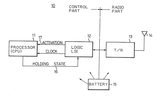
Figure 1 is a block diagram showing principle
construction of a mobile telephone terminal according to
the present invention. A mobile telephone terminal 10
of Fig. l is primarily classified into two parts, i.e.,
a control part and a radio part. The radio part is
mainly comprised of a transmitting and receiving (T/R)
unit 13 provided with an antenna 14. The control part
is mainly comprised of a processor unit (~PU) 11 and a
logic LSI unit 12. All are driven by a battery 15. The
present invention basically refers to the control part.
The members in the control part, including the processor
unit (CPU) 11 and the logic LSI unit 12, at least,
perform a variety of control functions. The functions
are classified into first control functions and second
control functions.
The processor unit 11 is provided to process the
first control functions, with the cooperation of
memories, which functions are not used frequently but
are complicated and operate at a high clock speed.
The logic LSI unit 12 is provided to process the
second control functions which are used constantly and
frequently with a low speed clock.
Further the logic LSI unit 12 is operative to
activate the processor unit 11 every time the first
control functions need to be handled by providing the
high speed clock (CLOCK) to the processor unit 11.
Figure 2 depicts a schematic flow chart for
1 3 ~ g
explaining the operation according to the present
invention. The words "ACTIVATION", "CLOCK" and "HOLDING
STATE", used in Fig. 1 will be clarified with reference
to Fig. 2.
Referring to both Figs. 2 and l, suppose that the
processor unit 11 finishes a certain process for
performing the first control functions, which is
expressed as "FINISH PROCESSING" shown at the top left
of Fig. 2. The processor unit ll then enters by itself
into a holding state ~refer to "ENTER HOLDING STATE" in
Fig. 2~. The holding state is notified from the
processor unit (CPU) 11 to the logic LSI unit 12 via a
line 16 (shown in Figs. 1 and 2). The logic LSI unit 12
then operates to stop supplying a master clock (refer to
"CLOCK" in Fig. 1) to the processor unit (CPU) 11. That
is no high speed clock is sent to the CPU 11 from the
LSI 12. Soon after this, the CPU and the cooperating
memories stop operating (refer to corresponding block in
the column of the CPU ll in Fig. 2).
Thus, the logic LSI unit 12 watches the status of
the processor unit 11 and stops the supply of the high
speed clock every time the logic LSI unit 12 detects
that the processor unit 11 is in the holding state.
It should be noted here that the power consumption
of the CPU 11 and the corresponding memories becomes
very low due to the nature of the CMOS devices, after
stoppage of the clock supplied to the CPU 11.
The logic LSI unit i2 continuously supervises
whether a processing to be achieved by the processor
unit (CPU) 11 is generated in the telephone terminal
(refer to the step "IS PROCESSING BY CPU GENERATED?" in
Fig. 2). If it is detected by the LSI 12 that the
related processing is generated, then the processor unit
(CPU) 11 is activated (refer to "ACTIVATION OF CPU" in
Fig. 2 and line 17 in Fig. 1). At the same time, or
preceding the activation of the CPU, the logic LSI
unit 12 resupplies the high speed clock (master clock)
1 3 1 ~ 8
(refer to "CLOCK" in Fig. 1) to the CPU 11. The CPU 11
then starts the related processing (refer to "START
PROCESSING" in Fig. 2), which will finally end again at
the step "FINISH PROCESSING". The above-mentioned
"ACTIVATION" is triggered preferably by issuing an
interrupt request to the CPU 11 from the LSI 12.
As understood from the above, the total power
consumption in the mobile telephone terminal is greatly
reduced, since the processor unit ~CPU) 11 and the
cooperating memories work intermittently, i.e., at a
relatively low frequency, wherein the processor unit 11
and the memories usually operate at a high speed clock
and thereby are high power consumption members.
Figure 3 is a block diagram showing an example of a
mobile telephone terminal according to the present
invention. In Fig. 3, reference numeral 11 represents
the processor unit as shown in Fig. 1, which unit 11 is
comprised of a main CPU having memories, i.e., ROM 18
and RAM 19 cooperating therewith. The main CPU 11 is,
2~ for example, an 8 bit microcomputer. The ROM 18 stores
therein a program to operate the processor unit (main
CPU) 11. The RAM 19 stores therein data for read and
write operations. As will be understood later, the
program in the ROM 18 should not be autonomous but
subject to an external command issued from the logic LSI
unit 12. Then CPU 11 and the memories operate at a
frequency of, e.g., 1 MHz (or 2 MHz), which frequency is
obtained by dividing in frequency the output signal from
a master clock source 25 of 4 MHz (or 8 MHz).
The logic LSI unit 12 is, in Fig. 3, comprised of a
main LSI 21 and a sub LSI 22 which are respectively
provided with a memory (ROM) 23 and a memory (ROM) 24.
The ROM 23 stores therein system information, for
example, a telephone number allotted to this mobile
telephone terminal and an area number of an area
determined under a contract between a user and a dealer.
The ROM 24 stores a serial number, for example, a
1 3 1 ~ ~ ~ 8
-- 7
production lot number of this mobile telephone terminal,
which lot number is determined by its maker when making
the mobile telephone number. It should be understood
that the logic LSI unit 12 is divided into the main
LSI 21 and the sub LSI 22 due merely to a factor in
actual design. That is, even though it is possible to
construct the logic LSI unit 12 using a single LSI, the
number of pins provided by the single ~SI chip becomes
extremely large. This being so, it is convenient to
construct the logic LSI unit 12 with two general purpose
LSI chips 21 and 22.
The mobile telephone terminal has further members,
other than the above recited members. Reference
numeral 30 represents the aforesaid radio part, as in
Fig. 1, comprising the transmitting and receiving (T/R)
unit 13 and the antenna 14. Reference numeral 40
represents a base band part which i5 mainly comprised of
a digital base band (D-BB) unit 41 and an analog base
band (A-BB) unit 42. The analog base band unit 42
contains therein, for example, analog filters, and deals
with analog voice signals. The voice signal is
communicated through a microphone 44 and a speaXer 4S.
A voice signal amplifier 43 is located therebetween.
Reference numeral 50 represents a man-machine
interface part which is mainly comprised of a sub CPU 51
of, for example, a 4 bit type, a display (DSP) 52, and a
key switch (KEY) S3. The display 52 acts as an
indicator. The key switch 53 contains function keys,
numeral buttons ("0" through "9"), volume switches, a
send command button, an end indication button, and so
on. All members are energized by the battery 15. For
saving the power of the battery 15, major members, such
as 11, 13, 18, 19 21, 22, 23, 24, 41, 42, are fabricated
using CMOS devices. The display 52, for example having
a 16 digit construction, is comprised of, for example, a
liquid crystal device which is, as is known, a low power
consumption device.
3 ~
-- 8 --
The sub CPU 51 controls the display 52 and the key
switch 53 periodically at 5 ms intervals. The
man-machine interface part 50 is constructed
exclusively, as in the prior art. The part 50 and also
the parts 30 and 40 are identical to those of the prior
art.
As mentioned above, the control functions performed
in the control part/ are shared by the logic LSI unit
and the processor unit. This will further be clarified
below.
Loqic LSI unit 12
I. Data reception processing
(a) Contents of the data reception processing
l~ Data reception processing
The data reception rate is:
lOK Baud, when the Advance Movable
Phone System (AMPS) is employed; and
8K Baud, when the Total Access
Communication System (TACS) is employed.
2) Decision by majority for words
Generally, the received data is composed
of words repeated, for example, 5 times, so as to
improve reliability of the data. In the example, a 3/5
majority is adopted. That is, if three normal bits
among five bits of located same position of each word
are obtained, the bit can be corrected.
3) Error correction of received data
Generally, a Bose-Chaudhuri-Hocqueghem
(BCH) code is utilized for the error correction of data
4) Decision by majority-for B/I bit
A busy/idle (B/I) bit is periodically
monitored in the mobile telephone terminal so as to
perform duplex communication. In the example, a 2/3
majority is adopted. That is, if two normal B/I bits
among last three B/I bits of receiving data are
obtained, the B/I state can be determined with the
result of majority noting.
131~8
g
5) B/I bit processing
In the processing, it is checked whether
it is possible to send data to the land station.
(b) Operation timing
The logic LSI unit 12 operates at each
interrupt sent at 100 ~s intervals to the processor
unit 11.
(II) High speed timer management
(a) Contents of the management
Many functions are achieved at respective
prescribed timings which are controlled by timers.
1) For example, if three kinds of timers are
managed, each of the timers has a resolution of 1 ms.
2) As another example, if seven kinds of
timers are managed, each of the timers has a resolution
of 10 ms.
(b) Operation timing
The logic LSI unit 12 operates at 1 ms
intervals.
To be specific, in Fig. 3, the main LSI 21 handles
the above-recited data reception processing, while the
sub LSI 22 handles the above-recited high speed timer
management.
Main_CPU 11
(I) Terminal control
A call origination, a call termination, and a
registration of the location of the mobile telephone
terminal are subjected to terminal control.
(II) Data transmission processing
(a) Contents of the processing
The data to be transmitted from the mobile
telephone terminal is processed by the main CPU 11.
(b) Operation timing
The operation is started any time the data
transmission is required.
(III) Low speed timer management
1 3 ~ 8
-- 10 --
(a) Contents of the management
As mentioned before, many functions are
achieved at respective prescribed timings which are
controlled by ti~ers.
1) For example, if six kinds of timers are
managed, each of the timers has a resolution o~ 50 ms.
2) As another example, if three kinds of
timers are managed, each of the timers has a resolution
of 2 seconds.
(b) Operation timing
The main CPU is operated by receiving an
interrupt given every 50 ms. To be specific, the
related interrupt request is generated in the sub
LSI 22.
Referring again to Fig. 3, the received signal
is input to the mobile telephone terminal by way of the
antenna 14 and the transmitting and receiving unit
(T/R) 13. The received signal is first supplied to the
analog base band (A-BB) unit 42 in which a filtering
operation is applied to the received signal. The thus
filtered signal is supplied, via the bus 20, to the
digital base band (D-BB) unit 41. The data from the
unit 41 is applied to the main LSI 21. As mentioned
previously, the main LSI 21 and sub LSI 22 cooperate
together.
The main CPU 11 is operated on demand
according to an activation by the logic LSI unit 12.
When the main CPU 11 is operated, the ROM 18 and the
RAM 19 also start operating in accordance with an access
thereto by the CPU 11.
The data to be transmitted from the CPU 11 is
transferred along a path opposite to the one mentioned
above. That is, the transmission data is transferred
from the CPU 11 to the antenna 14 through the main
LSI 21, the digital base band unit 41, the analog base
band unit 42 and the transmitting and receiving unit 13.
The logic LSI unit 12 watches a logic level on
131Q ~8
11 --
a bus available (BA) signal line 16 which is connected
between the logic LSI unit 12 and the processor unit
(main CPU) 11 and, when the logic level on the BA signal
line 16 assumes first logic level, e.g., logic "H"
(high), the logic LSI unit 12 detects that the processor
unit 11 is in the holding state. The logic "H" on the
line 16 is produced by executing a "Wait for interrupt-
instruction. In this case, the processor unit 11 enters
by itself into said holding state by an execution
therein of the "Wait for Interrupt" instruction
generated for each process when the aforesaid first
control functions are finished.
Thus, the main LSI 21 supplies the master
clock from the master clock source 25 or stops supplying
the same according to logic "L" (low) or "H" of the
signal BA (bus available) on the line 16 (a line for
transferring the master clock is not illustrated in
Fig. 3). The master clocX is supplied together with an
issuance of the interrupt request (IRQ). The logic LSI
unit 12 issues the interrupt request IRQ relating to the
aforesaid "Wait for Interrupt" instruction to the
processor unit ll, every time an interrupt request
(IRQ-R) occurs in the logic LSI unit 12, each of which
interrupts require an activation of the processor unit
(main CPU) 11.
Figure 4 is a brief circuit diagram of an example
of a timing control circuit. The timing control
circuit 60 is mounted in the logic LSI unit 12 and
produces the aforesaid master clock M-CLK and the
3~ interrupt request IRQ sent to the processor unit (main
CPU) 11 according to the input signals, i.e., the signal
~A and the interrupt IRQ-R.
Fig. 5 depicts a timing chart for explaining the
circuit of Fig. 4. The operation of the timing control
circuit 60 will be explained below with reference to
Fig. 5. The interrupt request IRQ is issued immediately
after the occurrence of anyone of the interrupts IRQ-R
131~9g
- 12 -
when the related interrupt occurs during a condition
where the logic level on the BA signal line 16 assumes a
second logic level, e.g., "L , which indicates that the
processor unit (main CPU) 11 is not in the holding state
but in the operating state. The interrupt request IRQ
is issued after a predetermined delay time ~rom the
occurrence of anyone of the interrupts IRQ-R when the
related interrupt IRQ-R occurs during the holding state
where the logic level on said BA signal line 16 assumes
the first logic level, e.g., "H".
The aforesaid predetermined delay time is a time
required for preparation of the high speed clock (1 MHz
or 2 MHz) which can normally drive the processor
unit 11.
The high speed clock is o~tained by dividing in
frequency the master clock M-CLK from the logic LSI
unit 12, at the source 25.
The logic LSI unit 12 contains therein a delay
means 62 which provides a delay conforming to the
preparation of the high speed clock which is lower than
the speed of said master clock M-CLK (4 MHz or 8 MHz)
produced by the master clock source 25 provided by the
logic LSI unit 12.
The master clock M-CLK is given to the processor
unit 11 via a first logic means 61 which receives two
inputs, one of which is the logic level on the BA signal
line 16, and the other of which is the interrupt IRQ-R.
The first logic means 61 operates to produce the
master clock, regardless of an existence of the
interrupt IRQ-R ("L"), when the logic level on the BA
signal line 16 assumes the second logic level, e.g.,
"L", while, the first logic means 61 operates to start
producing the master clock M-CLK, when at the occurrence
of the interrupt IRQ-R ("L") during a condition where
the logic level on the BA signal line 16 assumes the
first logic level ("H"), i.e., during the holding st~te.
The interrupt request IRQ is issued to the
~ 3 ~
processor unit ll via a second logic means ~delay means)
62 which receives two inputs, one of which is the logic
level on the BA signal line 16, and the other of which
is the interrupt IRQ-R.
The second logic means 62 operates to produce the
interrupt request IRQ immediately after the reception of
the interrupt IRQ-R, when the logic level on the BA
signal line 16 assumes the second logic level, e.g.,
"L", and produces the interrupt request IRQ after the
aforesaid predetermined delay time, when the logic level
on the BA signal line 16 assumes the first logic level,
e.g., "H".
In the first logic means 61, when the signal BA
assumes a logic level "L", and at the same, the
interrupt IRQ-R is generated in the logic LSI unit 12, a
NAND gate 63 produces an output of logic level "H".
Therefore, the master clock M-CLK is supplied from the
clock source 25 to the processor unit (main CPU) 11 via
an AND gate 64. The interrupt request IRQ is sent to
the processor unit 11, in response to the interrupt
IRQ-R, via the second logic means, i.e., delay means 62,
and a buffer gate 65. The processor unit 11 is then
activated and starts operating at the speed of, for
example, 1 MHz or 2 MHz. That is, the main CPU 11
divides in frequency the received master clock M-CLK
(4 MHz or 8 MHz).
When the BA signal assumes an "H" level, the master
clock M-CLK is stopped. The main CPU 11 is then stopped
from operating, as are the ROM 18 and the RAM 19.
When the BA signal assumes an "H" level, and at the
same time, the interrupt IRQ-R is generated in the logic
LSI unit 12, the interrupt request IRQ is issued after
an elapse of a predetermined time from the generation of
the interrupt IRQ-R. The reason why the IRQ is issued
after a certain elapse of time is that, if the BA signal
assumes a logic level "L", the main CPU 11 is under
operation (in an operating state), and therefore the
9 ~
- 14 -
main CPU 11 can ba immediately responsive to the IRQ.
Howevex, if the BA signal assumes a logic H', the main
CPU 11 is in the holding state, and therefore, a certain
delay time is necessary before an actual generation of
the clock which drives the main CPU 11. The delay time
is cre-~ted by the delay means 62. According to Fig. 5,
the delay time corresponds to four pulses of the master
clock M-CLK, the first pulse rises at the second change
of the IRQ-R. As mentioned before, in this embodiment,
the clock used in the main CPU 11 has a frequency of
1 MHz (or 2 MHz) which is obtained by dividing the M-CLK
of 4 MHz (or 8 MHz), by "4". Thus, the aforesaid four
pulses of the M-CLK correspond to the delay time.
Figure 6 is a circuit diagram of a detailed example
of the timing control circuit shown in Fig. 4. The
timing control circuit 60 of Fig. 4 has a construction
as shown in Fig. 6 and is mounted in the logic LSI
unit 12, particularly in the main LSI 21. The members
identical to those of Fig. 4 are referenced by the same
reference numerals and characters. The logic part 71
determines the issuance of the interrupt re~uest IRQ via
an AND gate 72. The AND gate 72 is opened after the
elapse of the aforesaid delay time. The AND gate 72
receives the output from a logic part 73 via a logic
part 74. The logic part 74 holds the output from the
preceding logic part 73 by means of a flip-flop (FF).
The logic part 73 produces the aforesaid delay time by
means of a counter which receives the master clock from
the clock source 25. When the higher 4 output bits in
the counter all go to a logic level "H", the output of
the logic part changes the status of the flip-flop (FF)
in the logic part 74 to open the AND gate 72. The
aforesaid counter is reset by an IRQ-RESET pulse which
is generated in the main LSI 22 so as to rapidly reset
the level of the IRQ line 17. If the level is
maintained at L" for a long time, it is impossible to
respond to the next IRQ. Accordingly, the level of the
1 3 ~
- 15 -
IRQ line 17 is returned to the usual state soon after
the issuance of the IRQ.
Figures 7A and 7B illustrate a block diagram
showing a detailed example of the main LSI 21 in Fig. 3.
The data bus 20 at the top left in Fig. 7A is connected
by 8 data lines D0 through D7, with the processor unit
(main CPU) 11. selow the data bus 20, an input address
bus is shown. An internal address decoder 82 specifies
internal registers 83 through 87 and also specifies, via
an address decoder 81, the external memories, such as
the ROM 18, the RAM 19 and so on (SUBLSI22, D-sB41).
The register 83 cooperates with a serial data out/in
unit 91 which handles the input data or output data to
be communicated with, via the sub CPU 51, the display 52
and the key switch 53. The main LSI 21 operates at the
low clock speed, for example, 96 KHz. The clock of
96 KHz is used, on one hand, after division in frequency
by a clock divider 92. On the other hand, the clock of
96 KHz is used for driving an internal interval timer 93
which controls a timer processing unit g4 and an IRQ
controller 95. The IRQ controller 95 also cooperates
with the IRQ processing register 84 which registers what
interrupt (IRQ-R) is generated. The unit 94 handles the
aforesaid high speed timer management. The
corresponding register 85 for the timer registers a
variety of management times, written by CPU ll. The IRQ
controller 95 receives a variety of interrupt IRQ-R.
One important IRQ-R is given from a BCH decoder 97
(Fig. 7B) which handles the aforesaid error correction
of the received data in terms of a BCH code. If the
data is received, the decoder 94 sends the IRQ-R to the
controller 95. Another IRQ-R is generated when, for
example, a battery problem occurs.
In Fig. 7B, the above-mentioned BCH decoder 97
receives data processed by members 101 through 105 which
commonly connect with a word synchronization detection
unit 106. The unit 106 is provided with the received
~3~ 39~
- 16 -
data (RDAT) and also the corresponding received clock
(RCLK). The member 101 handles the aforesaid decision
by majority for bits. The member 102 handles the
aforementioned decision by majority for the busy/idle
(B~I) bit. The member 103 is a word synchronization
protection unit which determines that word
synchronization is established when the synchronization
is detected two times successively, and on the other
hand, determines that the word synchronization is
maintained until the synchronization is not detected
five times successively. The members 104 and 105 are
timing generators for dealing with voice (V) channel
data and control (C) channel data, respectively, both
channel data will be explained later.
The member 96 is a master clock controller which
receives the aforesaid BA signal and sends the aforesaid
interrupt request IRQ and the master clock M-CLK. The
contxoller 96 also produces a clock of 1 MHz which is
used for another purpose and does not concern the
present invention.
Figure 8 illustrates a known data format of the
control channel data. The mobile telephone terminal is
always supplied with the data of Fig. 8 from a land
station when the mobile telephone terminal is put in a
waiting state for transmitting data. The data has
usually a speed of 10 Kbps. The mobile telephone
terminal detects an existence of data by finding a
dotting part composed of 10 bits having a bit pattern of
"1010 ... 10". The heading of the data is detected by a
word synchronization part composed of 11 bits having a
bit pattern of "11100010010 . As mentioned previously,
the words (40 bits) are transmitted 5 times repeatedly.
In actuality, each word portion is composed of a word A
part and a word B part. Either one of the words A and s
is allotted to respective user in advance by contract.
After the aforesaid decision by majority for the word A
(or word B), the aforesaid BCH (for example (40, 28; 5))
~31Q~
- 17 -
error correction is performed by the BCH decoder (shown
by 97 in Fig. 7B) to obtain 40 bit data. The numerals
(40, 28; 5) mean that each word is 40 bits in length,
among which 28 bits are used for inherent information,
and the error correction ability is at grade 5. Thus,
the correct word of 40 bits including 12 bits as parity
bits is stored in a 40-stage shift register (shown by 99
in Fig. 7B) and stored in a received data register
(shown by 87 in Fig. 7B). In Fig. 7B, the error
detected by the BCH decoder 97 is counted by an error
counter 98 and the result is stored in the error
register 86. The main CPU 11 determines whether the
data in the register 87 should be used or not by
referring to the result in the register 86.
Figure 9 illustrates a known data format of the
voice channel data. The voice channel data is supplied
as a burst from the land station. The data speed is
10 Kbps. In Fig. 9, "W.S." is an abbreviation of word
synchronization (WORD SYNC), "DOT." refers to dotting.
The bit patterns of the "DOTTING" and "~ORD SYNC" are
identical to those explained with reference to Fig. 8.
The heading of each data portion is detected with the
use of 101 bit dotting, by means of the digital base
band unit (shown by 41 in Fig. 3), and the unit 41 then
produces a preamble detection indicating a signal "PDI"
which is sent to the sub LSI 22. The sub LSI 22
receives the PDI signal and produces a guard pulse
(XGRD) to be sent to the main LSI 21. The guard pulse
is 103.2 ms which corresponds to the length of each data
portion. During the existence of the guard pulse, the
received data "RDAT" and the received clock "RDCLK" are
applied from the sub LSI 22 to the main LSI 21.
The main LSI 21 performs, when receiving the "RDAT"
and "RDCLK", the decision by majority and the BCH error
correction. At the end, the interrupt request IRQ is
sent to the main CPU ll, as mentioned previously.
Figures 10A and 10B illustrate a block diagram
~L 3 1 ~ 8
- 18 -
showing a detailed example of the sub LSI of Fig. 3.
The sub LSI 22 is also connected to the data bus 20 as
is the main LSI 21. An address decoder 121 functions
like the address decoder (shown by 82 in Fig. 7A). A0
through A3 are lower bits of the aforesaid address bus.
Characters "OE", "WE" and "XCE" denote an output enable
signal, a write enable signal and a chip enable signal,
respectively. The address decoder 121 specifies one of
the registers 122 through 126. The register 122 stores
a transmission OK signal and a transmission timing
signal from the CPU 11. The register 123 stores
inherent data to be transmitted and received from the
CPU 11. The register 124 stores control data for the
digital and analog base band units 41 and 42. On the
other hand, the register 125 stores data to be actually
processed by these base band units 41 and 42. The
register 126 stores channel selection data specified by
the CPU ll. The channel selection data, i.e., tuning
data, is sent to the transmitting and receiving unit
(T/R) (shown by 13 in Fig. 3) via a T/R serial data
transmission unit 127 which produces signals "SYNSTB"
(synthesizer strobe), "SYNCLK" (synthesizer clock), and
"SYNDAT" (synthesizer data).
A BB (base band) serial data transmission unit 128
cooperates with the registers 124 and 125 to produce
signals "ABBSTB" (analog base band unit strobe),
"DBBSTB" (digital base band unit strobe), "BBCLK" (base
band unit clock) and "sBDTA" (base band unit data),
which are sent to the digital and analog base band units
41 and 42.
A data transmission unit 129 cooperates with the
registers 122 and 123, together with a clock generator
(CLK GEN) 130 for data, to output the transmission data
to the digital base band unit 41. The unit 129 also
outputs a non-maskable interrupt (NMI) to the CP~ 11.
The NMI is different from the pxeviously mentioned
interrupt request IRQ. The NMI has the highest priority
~L 3 1 ~
-- 19 --
for transmitting data.
A split phase/non-return-to-zero converter
~SPL/NRZ) 131 is supplied with the received split phase
signal "RSPL" together with the master clock M-CLK and
the clock from the generator 130. Simultaneously, the
SPL/NRZ converter 131 cooperates with a phase-locked
loop unit (PLL) 132 for data which produces the received
data clock "~DCLK" to be sent to the main LSI 21.
The aforesaid "PDI" signal and the "XGRD" signal
are treated by a guard timer 133. The aforesaid clock
of 96 KHz for driving the main LSI 21 is output via a
stuffing divider 134 and a clock generator (CLK
GEN) 135. The divider 134 lowers the frequency of the
master clock M CLK to a certain frequency which is
lowered further to obtain a 96 KHz clock signal by the
generator 135.
As mentioned above in detail, the mobile telephone
terminal according to the present invention is very
useful for saving the power of the battery in the mobile
telephone terminal and extending the life of the
battery. According to an example, the current
consumption, in total, of the mobile telephone terminal
is reduced from 23 mA, which is a value of the prior
art, to 15 mA.