Note: Descriptions are shown in the official language in which they were submitted.
7 ~ ~
HYDROGEN ION MICROLITHOGRAPHY
BACKG~OUND OF THE INVENTION
1. FIELD OF l HE INVENTION
The invention relates generally to semiconductor lithography and pertains,
more specifically, to a hydrogen ion microlithography process.
2. DESCRIPTION OF THE PRIQI~ ART
Recently, there has been an extremely rapid gro~h in the application an~
fabrication of microelectronics. Microelectronics fabrication generally concerns
using conventional semiconductor lithography to produce various micrometer-
sized discrete semiconductor devices, integrated circuits and solid-state devices.
Generally, in semiconductor lithography, a high resolution integrated circuit
pattern is formed in a resist overlaying a semiconductor substrate. A permanent
micrometer-size device structure is formed with the resist pattern acting as a
~o mask by subtrac~ive etching or removal or oy addiLive deposition of metals or
insulators.
To continue, the application of microelectronics presently pervades virtually
all aspects of commercial, military, business and leisure activities. Moreover,
microelectronics has caused profound changes in such diverse fields as computers,
calculators, communications, entertainment, sports equipment and process~ontrol
'~
-2- ~3~ G'3~;
systems. Additionally, the size and performance of micrometer-size devices have
substantially improved through microminiaturization. Microminiaturization generally
describes the redu~ction in size of solid state devices to submicron level circuits through
semicollductor lithography.
For example, the sizes of electronic circuits in a pocket calculator have been
reduced from those that fit in a large, desk-top machine to those that fit on the head of
a pin. To take another example, a basic functional electrical element of a
microelectronic circuit is a transistor. Microminiaturization has made it possible to
fabricate thousands of transistors in a single chip. This reduction in transistor size has
also dramatically increased the operational speed of microelectronic circuits and has
lowered the cost per circuit by several orders of magnitude.
Despite this rapid growth, many applications need even higher performance
levels, higher functional density, higher reliability and lower production cost. Two
promising ways to achieve the desired goals have emerged. The first is by
submicrominiaturization, or making the microdevices even smaller. The second is by
making the integrated circuit chips as large as possible to stave off forming smaller
linesize, submicrometer geometries and device dimensions. Linesize generally concerns
the width of features at the resist, while the chip generally refers to the thin-film
semiconductor material on which the microcircuits are formed.
~o However, the need to produce larger chips is significantly limited by the defect
density of lithography processing operations. Defect density normally is associated with
an average densit~ of fatal defects or contaminates on the chip's surface. For example,
a dust particle usually leaves a pinhole with metal in a circuit line used for lift-off, and
sucll a det`ect can be the cause of a short. The defects can originate from the chip itself,
e~chillg, process equipment, storage boxes, personnel, human error or defects in a mask-
to~mask pattern. As the cllips
-3- ~iL 3 ~ ~ ~ 3 ~
become larger and the lines become closer, the nurnber and size of the defects
must be reduced for good yield.
Since the defect density limits the growth and size of the chip, producing
smaller microdevices with closer spaced, narrower features or lines is an
increasingly popular way to increase the functional density. The size of the lines
usually is a strong function oî exposure. Exposure normally involves subjecting
the resist to some form of electromagnetic racliationO The radiation causes a
differential change in some resist property such that specific line patterns can be
formed during resist deYelopment. As previously mentioned, development
o generally involYes the removal or additive deposition ot a metal or insulator. t~or
these reasons, exposing and developing the resist are dominant areas that provide
limitations to reducing the linewidths and the associated device dimensions. Thus,
concentration will be hereinafter focused on the needs and problems of the priorart from a resist and processing viewpoint.
To address the needs and problems of resist processing in submicrominiaturi-
zation, the microelectronic industry is attempting to refine the dominan$
semiconductor lithography or photolithography processing procedures.
Unfortunately, the desired smaller linewidths, submicrometer device dimensions
and geometries usually are beyond the capabilities of photolithography.
For example, a photolithographic mask usually contains an open or
transparent pattern. Ultraviolet light is transmitted thro~lgh the pattern to
expose corresponding resist regions fo! subsequent development. iJnfortunately,
diffraction effects from the mask openings and reflection effects within the resist
frequentJy legrade the quality of the replicated mask image. The diffraction
effects usually occur when the mask is separated ~rom the resist, when high
resolution is demanded and when the linewidth is reduced to being comparable to
the wavelength of the ultraviolet li~ht. Resolution generally concerns resolving
-4~ v ~
the finest linewidths associated with the wavelength of the ultraviolet light source.
Additionally, when the mask is placed relatively close to the resist, irregularities on the
resist often cause defects at the mask surface. Such defects frequently result in
corresponding defects in the next resist exposed with that mask.
To cope with the problems of diffraction, the microelectronic indllstry has
employed projection photolithography. Projection photolithography normally employs
a shorter radiation wavelength to expose the resist and a mask that forms an object in an
optical system. The optical system projects an image either in real size or demagni~led
onto tlle resist. The shorter radiation wavelength beneficially reduces the diffraction
10 effects. However, spherical aberration effects in lenses of the optical system normally
undcsirably limit the resolution of this replication process.
In an attempt to alleviate many of the aforesaid problems in photolithography, the
microelectronic industry has turned to high-energy (shorter wavelength) radiation
exposure systems. For purposes of the present application, high-energy radiation15 exposure systems are systems with an exposure energy greater than lOOO eV. The
conventional sources of such systems are electron beams (e-beams), ion beams and X-
rays, which use shorter wavelengths and higher energy photons. The high-energy
radiation sources can be employed to either focus a beam of electron energy to a spot or
cause the electron energy to be collimated and masked to flood expose the resist.
A number of publications discussing the use of such conventional exposure
systems include: an abstract entitled, Focused Ion Beam Scans Small Structure, Test &
Measurement World, p. 16 (1988); Darryl W. Peters, Keeping America Competitive,
Examining Competitive Submicron Lithography, Semiconductor International, pp. 96-lOO
~1988); Irwin Goodwin, Compact X-Rav Litho raphv
~ ! .
Machines Generate Hopc for Serniconductors, Physics Today, pp. 49-S2 (1988);
Joseph Grenier, Wafer Fabrica~ion Eguipment Five Year Fo!ecast, Solid Sta-te
Technology, pp. 67-70 (1988); and William Thurber, Photolitho~ra~hy's Heir StillNot Obvious, Says Interface Keyns)te, Semiconductor In~ernational, p. 15 ~1988).In e-beam lithography9 which is normally considered the dominant high-
energy radia6ion source, the beam exposes the resist where it strikes and locally
changes its characteristics. Subsequent resist development can either selectively
remove the exposed resist regions or remove the unexposed regions. However,
proximity effects are the primary limitation that prevents obtaining sa~isfactory
linewidths with the e-beam lithography. Proximity effects describe pattern
fidelity degradation. This degradation is primarily caused by electron scattering
and secondary electron generation in the resist and the chip. For instance, the
proximity effects create an exposed volume of resist that is wider than the
diameter of the impingent beam.
In X-ray lithography, continuous X-rays are normally produced by electron
bombardment of a fixed or rotating anode. Unfortunately, faster organic resists
are usually required since the X-ray sources are frequently too weak for presentsingle-film organic resist. For example, generally, no practical single-film
organic resist can be exposed rapidly enough to be competitive with projection
photolithography.
Likewise, conventional ion lithography, as opposed to the hydrogen ion
microlithography of the present invention, suffers problems similar to ~hose of
X-ray lithography. These problems are also usually associated with the newer
emerging projection ion lithography. For these reasons, the application of
~5 conventional high-energy radiation exposure sources such as ion beam lithography
is often restricted to fabricating, measuring and repairing photo mask. The
publication of T. D. Cambria and N. P, Economou, Mask and ~e~lh
-6~ ,s ~
Focused-lon Beams, Solid State Technology, pp. 133-136 ~Ig87), explains the use of
focused-ion beam technology for mask and circuit repair.
The exposure, development and processing problems relating to organic-
based resist have motiva~ed the microelectronic industry to look for a resistless
process. A resistless process would directly form circuit components and
eliminate all the resist process steps. Cienerally, the major conventional energy
sources existing in resistless, lithography technology are high-energy X-rays,
lasers, e-beams and ion beams. However, resistless lithography is comparatively
in its infancy. Moreover, the beams of ~he major high-energy sources normally
0 are difficult to spread over large surîace areas.
Several solutions to the problems associated with organic resist exposure,
development and processing are disclosed in U.S. Pat. Ser. Nos. 4,5691124;
4,601,778; 4,615,904; and 49377,437. For example, U.S. Pat. Ser. No. 4,56g,124
discloses forming thin conducting lines in a two-layered inorganic material such as
silicon or aluminum overlying a layer of refractory metal with a high-energy, ion-
beam implantation source. The tw~l~yered n aterial behaves as a resist. In U.S.
Pat. Ser. No. 4,601,778, portions of a polysilicon film are initially exposed toeither an oxygen plasma or a hydrogen plasma, and thereafter, the entire
polysilicon film is exposed to a polysilicon etchant and etched without the need to
employ a mask. In U.S. Pat. Ser. No. 4,615,904, a patterned film is deposited onto
a substrate using a laser energy source or a low-power, focu~ed e-beam source~
Lastly, in U.S. Pat. Ser. No. 4,377,437, a high-powered ion source for implanting
indium, gallium or gold ions is used to define features directly on an inorganiclayer of a solid-state precursor device9 for example, SiO2 or Si3N~;, which serves
as a mask.
In a development involving gallium ion implantation, P.H. La Marche and R.
Levi-Setti, Amorphous silicon as an~anic resist, SPIE Vol. 471, Electron-Beam
-7~ v~
X-Ray and lon-Bearn Technique for 5ubmicrometer Lithographics 111, pp. 60-65
(1984), discloses that negative tone images can be produced in g low-discharge
amorphous silicon hydride by selective gallium-ion implantations. Also, the
gallium implanted amorphous silicon exhibits a greatly reduced etch rate.
Regarding the concept of reducing the resistance to etchants through ion
implantation, the publication of P.A. O~Connell, ~ormation of ResistiYe Films hYlon ~ombardment, Colloquium on lon Implantation, London England, p. 7 (19 _)
discusses the formation characteristic o~ resistance in aluminum films subjectedto oxygen ion bombardment.
1~ The present invention, however, represents yet another different
development and solution, which employes a low-energy hydrogen ion source, and
which results in unexpected improved microlithography process procedures,
particularly with respect to eliminating all of the organic resist process steps.
The attributes of the present invention are reflected in the following objects.
1~
SlJMMARY OF THE lNYl~NTlON
Against the foregning background, it is a general object of the present
invention to provide a low-energy, hydrogen ion microlithography process that
'o overcomes many of the aforesaid shor~cornings and disadvantages associated with
prior art organic resist used in conventional lithography processes.
It is a specific object to use hydrogen ion microlithography as a means to
effect patterning without the need fnr employing an organic resist.
It is another specific object to use hydrogen ion microlithography as a means
~S to permit amorphous silicon or hydrogenated amorphous silicon to serve as an
inorganic single-layered resist.
~,, 6~ 3
-8-
It is a further specific object to use hydrogen, ion microlithography as a meansto permit a single layer of thin-film amorphous silicon or hydrogenated amorphous
silicon to serve as a positive or negative resist.
It is still a specific object to use hydrogen ion microlithography as a means to5 permit a single layer of thin-film amorpllous silicon or hydrogenated amorphous silicon
to serve as a resist that is suitable for development by either a wet developer or a dry
developer.
It is yet and still a specific object to use hydrogen ion microlithography as a
means to directly pattern amorphous silicon or hydrogenated amorphous silicon as a
10 means to substantially eliminate many of the clean room operations required when
employing organic resists.
The above objects, as well as still further objects and advantages, are obtained by
the present invention by providing an ion microlithography process for use in
microelectronic fabrication and semiconductor device processing. The process includes:
15 providing a single layer of either an amorphous silicon or a hydrogenated amorphous
silicon material. A pattern is recorded in a selected one of the single layers of
amorphous silicon or hydrogenated amorphous silicon by preferentially implantinghydrogen ions therein so as to permit the selected layer to serve as a resist suitable for
subsequent development. Finally, the selected layer is developed to provide a surface
2 0 pattern therein adaptable for subsequent use in microelectronic fabrication and
semiconductor device processing.
BRIEF DESCRIPrION OF THE DRAWINGS
The accompanying drawings, which are incorporated in and form a part of the
specification, illustrate preferred embodiments of the present invention and together with
25 the description serve to explain the principles of the invention, wherein:
_9~ e~ ~
FIG. 1 is a par~ly broken~ enlarged, cross-sectional view of a chip comprising
a selected layer of ei~her amorphous silicon or hydrogenated amorphous silicon
being subjected to ion implantation frorn a low energy, hydrogen ion source in
accordarlce with the in~ention~
FlGo 2 is a broken, enlarged9 cross-sectional view of the chip of FIG. I after
positive development.
FIG. 3 is a broken, enlarged7 cross-sectional view of the chip of FIG. I after
negative development.
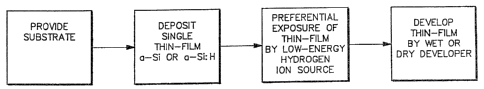
FIG. 4 is a flow chart illustrating the general process steps used in the
hydrogen ;on microlithography of the present invention.
FIG. 5 is an example of a pattern of dots in a positive functioning sin~le
thin-film layer of hydrogenated amorphous silicon fabricated using the low-energy
hydrogen ion source of FIG. 1.
FIG. 6 is an example of a collection Of a variety of line patterns in a positivefunctioning single thin-film layer of hydrogenated amorphous silicon fabricated
using the low-energy hydrogen ion source Of FIG. 1.
IDEl AILED DESCRIPTION O~ THE PREFERRED EMBODIMENTS
Referring now to the drawings and especially to FIGS. 1-4, the present
invention uses low-energy hydrogen ion microiithography as a means to
preferentially expose and pattern a selected thin film of either amorphous silicon
or hydrogenated amorphous silicon for subsequent rnicrodevice fabrication and
semiconductor processing without the need of an organic resist. In practicing the
inventionj a chip lO having a substrate 12 and a single starting thin-film layer 14
is formed and processed.
-10- ~a~4
As is best illustrated in FIGS I and 4, the substrate 12 is initially provided to
support the thin film 14. Depending on the application and ultima~e use of the
processed chip 10, the substrate 12 may preferably be a low-cost metal7 a glass, or
a plastic material. For instance, in integrated-circuit manufacture applications,
the substrate 12 preferably comprises a single-crystal semiconductor material
with or without an oxide layer. An example of such two materials are silicon andgallium arsenide. ~or large-area, display circuit, manufacture applications, thesubstrate 12 preferably comprises a semiconductive or a conductive thin film
layer, which is itself deposited on a substrate.
Following the formation of the substrate 12, it is one feature of the present
invention to form the base or starting thin film 14 from either an amorphous
silicon material or a hydrogenated amorphous silicon material. The amorphous
silicon or its hydrogenated form is used as the base material for several reasons.
Some of these reasons concern the development and exposure properties of the
thin film l4, as will be more fully described hereinbelow.
Any number of conventional deposition processes sùitable for depositing a
single thin film 14 of amorphous silicon or hydrogenated amorphous silicon to a
thickness of less than about 1 micrometer (10~6m) may be employed. When
amorphous silicon material with little or no hydrogen content therein is chosen for
the base layer 14, it may be deposited, for example, by sputtering, photochemical
vapor deposition, physical vapor deposition, homogeneous chemical vapor
deposition (CVD) or light-induced CVD using infrared lasers. Preferably, a high-quality amorphous silicon layer is deposited onto the substrate 12 under a vacuurn
by plasma-assisted CVD or glow discharge CVD.
n,~; When a hydrogenated amorphous silicon layer is selected for the base layer
14, it can be formed in one manner by concurrently introducing the hydrogen and
silicon atoms therein. For example, photoinduced CVD is one suitable deposition
process ~or introducin~ atomic hydrogen into the amorphous silicon during its
growth ~o produce a hydrogenated amorphous film. Preferably, radio frequerlcy
~RF~ ~low-discharge CVD is used for this purpose.
Alternative1y, the desired hydrogena~ed amorphous silicon layer may be
formed by introducing the hydrogen atoms therein ~fter the deposition of the
amorphous silicon layer through post-hydrogenation or rehydrogenation. Post-
hydrogenation generally involves the process of introducing the hydrogen atoms
into an amorphous silicon material that was originally deposited with liLtle or no
hydrogen content. Rehydrogenation generally concerns the process of
reintroducing hydrogen atorns into an amorphous silicon material that was
originally hydrogenated during its deposition with the hydrogen content having
been subsequently driven out by heating. It will be noted that the pos~-
hydrogenation and ~he rehydrogenation operations are normally performed while
the thin film 14 is being preferentially exposed for subsequent development, as
will be more fully described hereinafter.
RF-generated hydrogen plasma, direct-current (DC) hydrogen plasma and
microwave-excited hydrogen plasma are suitable processes for providing a desiredbase layer 14 of hydrogenated amorphous silicon through post-hydrogenation.
Preferably, and in accordance with the process of the invention, post-
hydrogenation process is perforrned by using a low energy hydrogen ion source.
Similarly, rehydrogenation is prefer~bly performed by usin~ a low-energy,
hydrogen, ion source with an RF glow-discharge deposited, starting and
hydrogenated amorphous material.
To effect post-hydrogenation and rehydrogenation, any conventional
hydrogen ion source 16 suitable for providing a low implantation energy may be
used. A suitable implantation energy is in a range of from about 300 eV to about1000 eV. A suitable current density is in a range of from about 0.1 mA/cm2 to
about 2û mA~cm2. These ranges ensble the electrical, optical and photosens-
itiYity properties of amorphous silicon films upon hydrogenation to be enhanced,
as will be more fully described hereinafter. A particularly preferred hydro~en ion
source 16 is the Kaufman lon Beam System marketed by Commonwealth Scientific
Corporation under the trademark Millatron IV.
It will be appreciated that the specific details of the Kaufman lon Beam
System have been omitted from the drawin~s for the sake of clarity, since the
system is well known in the art. Even so, the system will be briefly described.
The Kaufman lon ~eam System is equipped with a ~urbomolecular pump and a
lo chamber which can be evacuated to a base pressure of about 2 x 10⁻⁶ Torr~ The
system has provisions for back filling with hydrogen to an operating pressure of
about 8 x 10 4 Torr. The hydrogen ions are produced in the system by bombarding
with high energy electrons. The hydro~en ions are then accelerated and
collimated through a stainless steel grid assembly to produce ion beams with
energy that can be adjusted to any desired level up to a maximum of 2000 eV.
Having described the details of the ion source 16, a brief illustration of the
rehydrogenation and post^hydrogenation operations will now be given. These
illustrations will provide a better understanding of the importance of using
amorphous silicon or its hydrogenated form as the base layer 14. This
understanding or explanation is with respect to the structural changes and
development properties curring in the base layer 14 during the rehydrogenation
and post-hydrogenation operations and during exposure.
Turning first to the post-hydro~enation processes, in this particular
illustration initially, a thin film 14 of undoped amorphous silicon is preferably
;~5 desposited by RF glow-discharge under a vacuum onto a high-resistivity,
crystalline silicon or glass substrate 12. The substrate is deposited to a thickness
of about 500 nm with a substrate temperature of about 480C. Thereafter, the
~ 3 ~
deposited amorphous silicon is bombarded by hydrogen at least once. For this purpose,
a preferred implantation energy is from about 500 eV to about 600 eV and a preferred
current density is about 1 mA/cm2. Lastly, the resulting hydrogenated film is annealed
at a temperature of about 300OC in a vacuum for about 2 hours.
Turning now to the rehydrogenation process, in this particular illustration, an
intrinsic thin film base layer 14 of hydrogenated amorphous silicon is initially deposited
by RF glow discharged onto a high-resistivity crystalline substrate to a thickness of abo!Jt
500 nm at a substrate temperature of about ~500C. It should be specifically noted that
the invention contemplates practicing rehydrogenation with starting materials that are not
lû fabricated with the ion source 16, as will become more apparent hereinafter. Thereafter,
the hydrogenated amorphous silicon layer is annealed to a temperature of about 500oC
for about 10 hours. The annealing causes dehydrogenation or outgassing of the
11ydrogen.
Next, the dehydrogenated film is bombarded by low-energy hydrogen ions at least
once at a preferred dose of from about 300 eV to about lO00 eV. A preferred
implantation time is about 60 minutes, while a preferred current density is about 1
mA/cm2. Lastly, a rehydrogenated film is anne~led at a temperature or around about
~OO~C in a vacuum for at least 1 hour. While post-hydrogenation and rehydrogenation
have been described in connection with two particular illustrations, one skilled in the art
will appreciate that thepost-hydrogenation and rehydrogenation operating parameters and
process steps are not necessarily so limited.
As is best shown in FIGS. 1 and 4, it is another important feature of the present
invention to preferentially or selectively expose the thin film 14 with a low-energy
hydrogen ion source. The film 14, as previously mentioned, comprises a selected thin
film layer of amorphous silicon or hydrogenated amorphous
.
silicon. The preferential exposure functions to directly write or transfer a high-
resolution, circui~ image or line pattern onto the film 14 for subsequent
development. The exposure operation also functions to provide a means to
enhance or to improve the electrical, optical and photosensitivity characteristics
of the selected thin-film 14 material, if so desired for subsequent applications.
Any conventional hydrogen ion source 16 suitable of providing a iow
implantation energy of from about 300 eV to about 1000 eV may be employed to
preferentially expose the deposi~ed chosen layer 14. A preferred ion source 16 for
this purpose is the previously described Kaufman lon Beam System.
The exposure of the thin film 14 follows the filrn deposition. The exposure
can be performed in a well-known manner either by focusing a beam of ions 1~ to
a spot or by collimating and masking the beam 18 to flood expose the chip 10. Itwill be appreciated that the specific details of the ion beam mask have been
omitted from the drawings for the sake of slarity, since general principles of ion
beam mask are well known in the microlithography art.
The preferred implantation energy is some discrete value between about
300 eV and 1000 eV, while the preferred current density is some discrete value
between 0.1 mA/cm2 and 20 mA/cm2. These implantation ranges are required to
provide the necessary structural and chemical changes in the base layer 14, which
2~ changes allow the desired developmental properties of the layer 14 to be reali~ed,
as will be more fully explained hereinafter. Also, the beam diameter should be at
least about 10% larger than a diameter of the exposed chip 10 in order to provi~le
~atisfactory process uniformity.
It has been found in practice that the exposure and development properties
are different for hydrogenated amorphous silicon materials formed by pos-l-
hydrogenation or by rehydrogenation using the ion source 16. This difference is
with respect to the properties of, first, amorphous silicon films having little
-lS-
~ s, ~ ~ r~
hydrogen therein and, second, hydrogena~ed amorphous silioon films, both of which
have been formed by other deposition methods. MoreoYer, these differences
contribute to allowil~g the single layered thin-film 14 to advantageously flexibly
function as a negative or positive inorganic resist and a mask. Simply stated, anegative resist retains the exposed regions after development, while a positive
resist retains the regions not exposed after developmen~.
To explain, preferentially exposing a thin film 14 of amorphous silicon or
hydrogenated amorphous silicon that was not originally hydrogenated with a low-
energy hydrogen ion source causes important chemical and structural changes in
1~ these films. These changes result from the absorbed or implanted hydrogen atoms
and the associated effects they cause upon being diffused into the ~ilm 1~. lhe
effects of diffusion involve the amount and arran~ement of implanted hydrogen inthe film, as well as the type of alloys or bonds formed therein. They also involve
the semiconductor properties and the development proper~ies of the exposed film
~5 14. Thus, as previously mentioned, it is seen that the bonding configuration and
the amount and distribution of ` the implanted hydrogen atoms differ in
hydrogenated amorphous silicon material formed with a low-energy ion source
than with hydrogenated amorphous silicon formed with other methods.
For instance, when the thin film 14 is thicker than a range of penetration
from the bombarding or impinging hydrogen ions 18 of the ion source 16, the front
surface 20 in the specific regions where it is bombarded accumulates substantialamounts of the absorbed hydrogen. More specifically, from about 15 at. %
hydrogen to about 30 at. ~6 hydrogen accumulates in the flrst 100 nm of the front
surface 20 of the film 14, where it is specifically irradiated. Consequently, the
~?5 hydrogen accumulating at the front surface 20 is substantially more than that
accumulating at the back surface ~2.
J
--16--
lt is evident that ~he hydrogen absorbed by the film 11~ and accumulatinæ at
the front and back surfaces 20 and 22 depends on the diffusion property of ~he
implanted atomic hydrogen. This diffusion property is generally a function of
temperature and the structure and composi~ion of the film 14. Incidentally,
because of the diffusion process, the hydrogen accumulating at the front surface20 decreases exponentially toward the back surface 22.
Additionally, monohydrides or silicon-hydrogen (Si-H) bonds form ~he
dominant bonding configuration where the impinging hydrogen of the low-energy
ion source 16 strikes the pure amorphous silicon and the hydrogenated amorphous
silicon film materials. In this way, the îront surface 20 becomes substantially
saturated with the silicon-hydrogen bonds. Since silicon-hydrogen bonds
substantially prevent or retard the oxidation process of a filrn surface exposed to
oxygen, it follows that the silicon-hydrogen bond enriched front surface 20
functions to significantly impede a removal or etch action of particular developers
as described below.
For example, some particular wet developers can etch or remove desired
regions of pure amorphous silicon and hydrogenated amorphous silicon films in a
two-step oxidation reaction and oxide etching process, when such films are not
formed using the low enersy of the hydrogen ion source 16. However, this
oxidation reaction and, thus, the etching thereof are substantially impeded wi~hthese same wet developers, when identically fabricated films are exposed or
hydrogenated with the low energy of the ion source 16. As mentioned previously,
the retarding action or stop etch effect occurs, in part, because the front surface
20 is saturated with the silicon-hydrogen bonds introduced by the low-energy
hydrogen ion source 16.
Similarly, some particular dry developers will remove the specific regions of
the film 14 preferentially exposed by the ion source 16, while not removing the
--17~ s
non-exposed back~ round regions. This happens because of the chemical and
structural film changes resulting from exposing the film 14 with the ion source
16. With these dry developers, specific film regions are initially provided withsurface oxides. The surface oxides function to assist in preventin~ the removal of
the background film re~ions not exposed by the ion source 16. The formation of
the surface oxides at specific film regions are achieved by, firstly, oxidizing the
surface of a dehydrogenated amorphous film 14. Thereafter, the surface oxides
are selectively remoYed, and the film 14 is preferentially irradiated with hydrogen
ions, as will be more fully explained hereinafter.
Thus, specific film regions chemically and s~ructurally changed ~y the
~bsorbed hydrogen, or by the absorbed hydrogen in conjunction with an oxide
enriched surface, becom~ resistant to some particular wet and dry developers. inparticular, these changed film regions become resistant to a number of developers
that can nQrmally remove the pure amorphous silicon and the hydrogerla~ed
amorphous silicon ~ilms having certain film characteristics. A few characteristics
that enable such removal concern: the uniform distribution and disposal o the
implanted hydrogen a~oms in these films; and film surfaces that are not saturated
with silicon-hydrogen bonds or with a combination of these bonds and the surfaceoxides.
Said somewhat differently, some developers cannot remove the specific fihn
regions exposed by a low~nergy hydrogen ion source. Or, such developers can
only remove the exposed film regions at a substantially slower removal rate thanthe rate at which they normally remove amorphous silicon and hydrogenated
amorphous silicon film regions not exposed or hydrogenated with a low-energy
hydrogen ion source. It is obviousj however, that those developers that can
normally remove or etch amorphous silicon or hydrogenated amorphous silicon
film regions unaltered by the exposure effects of the ion source 16 still have this
type of removal capability.
-18~ ,;,3 jj 1
HaYinE~ described the details of hydro~en ion exposure, reference is made to
FIG. 2 where it is best shown that after exposure, some developers will allow the
single-layered thin film 14 to function as a negative resist 14a. The film l/~a
functions as a negative resist because, as mentioned earlier, the hydrogen-
irradiated re~ions 2S remain after development, while -the non-irradiated regions
28 are removed. In B like manner, as is best shown in FIG. 3, after exposure, other
particular developers will allow removal of the hydrogen-irradiated regions 26 of
such films, while allowing the non-irradiated regions 28 to remain. Thus, the
single thin film 14 is caused to function as a positive resist 14b.
It îollows that the preferential exposure with the low-energy hydrogen ion
source 16 constitutes a method o forming high-resolution features, lines or
surface structures. Moreover, these features, lines and structures are useful for
applications as a microcircuit image or pattern employed in microdevice
fabrication and semiconductor processing.
It will now be understood that performing rehydrogenation and post-
hydrogenation operations with a low-energy hydrogen ion source 16 normally
enables the resulting hydrogenated amorphous silicon film to undergo structural
changes similar to those oscurring in the exposed thin film 14. lhis holds true in
rehydrogenation provided the starting hydrogenated amorphous silicon film was
~20 not fabricated with a low~energy hydrogen ion source. Moreover, it will befurther understood that performlng low-energy, post-hydrogenation and
rehydrogenation operations on the chip 10 with the ion source 16 will normally be
performed while concurrently ~xposing the thin film 14.
Attention is now drawn to the fact that heretofore persons skilled in Ihe
microelectronics art were not aware that a low-energy, hydrogen ion source 16
could be used in the new manner contemplated by the invention. The new process
utilizes the hydrogen ion source 16 to preferentially expose single thin films ol
-19- ~ -7 ~
amorphous silicon or i~s hydrogenated rorm. Such exposure provides a new and
useful inorganic, single-layered negative or positive resist suitable for dry and wet
development, as will become even more apparent hereinafter.
It will be apprecia$ed that ~he present invention also contemplates using the
exposure operations of the hydrogen ion source 16 to advantageously enhance or to
improve the electrical, optical and photosensitivity properties of the thin film 14
during exposure, rehydrogenation and post-hydrogenation. The photosensitivity ofa hydrogenated amorphous silicon film is usually expressed by the AMI photo-to-
dark conductivity ratio. The photoconductivity relates to the photogeneration,
10 transport and recombination s~ electrons ar:d holes. Lastly, the optical properties
generally involve the optical band gap and transmission. To continue~ the desired
properties can frequently be enhanced or improved by ion-beam hydrogenation
with respect to similar properties obtained wi~h most conventional hydrogenationprocesses, such as E~F glow discharge hydrogenation.
As previously mentioned, ~he photosensitivity and other semiconductor
properties of tlIe thin films of amorphous silicon and hydrogenated amorphous
silicon are usually strongly effected by srnall changes in their structure and
chemical composition. In general~ a number of detrimental changes are frequentlycaused by the manner in whish the impinging ions during exposure, pos~
hydrogenation and rehydrogenation act on the semiconductor thir film 11~
Generally, the ions act through sputtering and radiation damage. In practicing the
invention, a number of process operations importantly contribute to minimize
sputtering and radiation damage, as well as to minimize other detrimental ef~ects
that degrade the electrical and semiconductor properties.
For example, hydrogen as above mentioned, is the lightest element in the
Periodic Table. Consequently, hydrogen substantially minimi~es radiation and
sputter damages when it is implanted into the film 14 with a low-energy hydrogen
3 ~
-?0_
ion source such as at 16. Moreover, it is found in practice that the acceleration
associated with the generated hydrogen ions from the ion source 16, substantially
facilitates the penetra~ion of the ions into the film 14. Hence~ the diffusion of
the hydrogen ions from the front surface 20 to the back surface region 22 of the
film 14 is readily accomplished. Consequently, hydrogenation performed with the
low-energy ion source 16 is normally substantially more efficient. This efficiency
is with respect to hydrogenation performed with other methods that provide iess
acceleration of the hydrogen ions, such as the prior art RF-hydrogenation method.
Also, the implanted hydrogen acts to passivate the exposed thin film 14, and
1~ thus, acts to enhance its photoconductiYity. The implanted hydrogen functions to
enhance the photoconductivity because generally the hydrogen content of the film
14 is increased. Moreover, the increased level of hydrogen functions to remove
localized states and to modify an energy gap of the ~ilm material by removing the
localized states therefrom.
~5 Additionally, using the amorphous silicon or its hydrogenated form as an
inorganic resist advantageously elimina~es all the problems associated with
defects derived from organic resist processing. Moreover, low defect processing
is advantageously enhanced by performing the fabrication and exposure operations
of the chip 10 in a vacuum. Also, such an inorganic resist advantageously
eliminates all the remaining non-contamination control process steps associated
with conventional organic resist exposure, development and processing. Lastly, it
is evident that eliminating the organic resist process operations advantageously
reduces the cost of fabricating devices contemplated by the present inven~ion.
Incidentally, the publication of Y.S. Tsuo, E.B. Smith, and S.K. Deb, lon
3 Beam~ydro~enation of AmorPhous Silicon, Appl. Phys. Lett. 51 (l8)J PP. 143~;-
1438 (1987) provides a more complete explanation of the nature and extent to
which some properties can be improved through rehydrogenation using a low-
energy hydrogen ion source. In ~his instance, photo-to-dark-conductivity ratios as
high as 5.6 ~ 105 at air mass one with hydro~en-impianted materials were obtainPd
with the Kaufman lon Beam SystemO Also, by way of background, this publ;cation
points out that light-induced reduction of the photo- and dark conductivities in the
rehydrogenated materials after 20 h of AM I illumination were eliminated. Las~ly,
improvements in the optical band gap and an abili~y to controllably incorporate
more hydro~en into the rehydrogenated material then was originally deposited by
glow discharge was achieved.
It is now apparent that when the selected base thin film 14 is amorphous
~0 silicon, it can be advantageously provided with substantially high photosensitivity
properties and stability properties durin~ lhe exposure or hydrogenation processoperations. Moreover, the optical properties can be precisely controlled, while
the electrical and photosensitivity properties of the specific thin ~ilm regionshydrogenated or exposed by the ion source 16 can be enhanced or improved.
1~ Incidentally, it should be noted that the control of the optical propertles
adYantageously enables the present Invention to be used in the fabrication of
amorphous silicon memory devices.
Following the exposure of the chip 12 to hydrogen, it is yet another
important feature of the present imention to employ the selected single thin-film
~0 layer 14 as an inorganic mask-resist, This mask-resist, significantly, is suitable
lor de~elopment by wet or dry developers. As previously mentioned, during the
preferential exposure of the thin film 14, the exposed regions 20 are structurally
changed to record a pattern tl?erein for subsequent development. By recording the
pattern lines, it is apparent that the inorganic, mask-resist functioning thin-film
a.~ 14 is useful for subsequent microdevice fabrication that requires a pat~ern
definition.
-22~ r ~ "9
As is best shown in FIGS. ~, 3 and 47 it is still another feature of the presentinvention to employ both dry and wet developers following exposJJre. \Yet
development generaJly invol~res a liquid or solvent etching through oxidation-
reduction reactions from metals and ~isplacement. I~ry development generally
involves solventless development by sublimation or vaporization of the resist
material through direct irradiation or by using a reactive plasma gas to
differentiate the image. The plasma gas may be described as a conductive gas
with equal densities of positively and negatively charged particles and excited
neutral radicals.
A suitable wet developer for etching the exposed selected single layered Vlin
film 14, when it is functioning as a positive resist 26, is a solution of isopropyl
alcohol (IPA), potassium hydroxide (KOH) and water (H2O) with about ~ wt % or
more IPA, about 20 wt % KO~I and about 55 wt % H20.
Additionally, a suitable wet developer for etching the exposed film 14, when
it is functioned as a negative resist 24, is a solution of KOH, IPA, and H2O w.th
about 24 wt % KOH, about 13 wt % IPA and about 63 wt % H2O.
A suitable dry or solventless developer employed to develop the exposed
single-layered thin film 14, when it is acting as a positive resist 30, is an RF-
generated hydrogen plasma. The dry development ot ~he film 14 when it is
functioning as a positive resist is preferably performed with the RF-generated
hydrogen plasma. However, it shou1d be understood that other suitable dry
developers having adequate characteristics to effect sublimation oE the exposed
film 14 or to chemically differentiate the patlern thereon when the film l4 is
functioning as a positive or negative resist may be employed, as will occur to
~5 those skilled in the art.
Similarly, wet developers other than the IPA + KOH ~ H2O etchants
described hereinabove, ha~lng the adequate characteristics to remove the exposed
3 d ~ ~
regions or unexposed regions of the thin filrn 14 at a rate faster than its
background and in a controlled manner may be employed, as will occur to those
skilled in the art.
The followin~s examples serve to illustrate certain preferred embodiments of
the present invention and are not to be construed as to limiting the scope of the
present invention.
EXAMPLE 1.
First, a base intrinsic hydrogenated amorphous silicon ~hin film 14 was
deposited by RF-8lOW discharge on a 2.54 cm by 2.54 cm glass substrate at a
2S0C substrate temperature in a load-locked, single-chamber sys~em to a
thickness of about 400 nm. The optisal band gap of the starting hydrogenated
amorphous silicon film was about 1.7S eV, while the photo-to-dark conductivity
ratio was about I x 106. The base film was then heated at about 540C in a
1.~ 10-6 Torr vacuum for approximately 10 hours to outdifuse the hydrogen.
Next, the hydrogen ion 50urce 16 with an energy of approximately 600 eV
and a current density of approximately 0.24 mA/cm2 was masked to preferentially
expose and pattern the base film for about 4 hours at a temperature of about
250C. Lastly, a wet developer comprising a solution of IPA (13 wt 96), KOH (24
wt %) and H;~O (63 wt %) was employed to develop the speciic pattern of the
hydtogenated amorphous silicon film.
It was found that the exposed portions of the preferentially hydro~enated
amorphous silicon film did not etch. However, the unexposed portions thereo~
were uniformly etched or removed (ne~ative) at an etch rate of about 10 nm/
~5 min. Additionally, patterns about l x 10-6 m wide with very lilttle undercuttin~ of
the film were produced. Scanning electron microscopy was employed to detec~
localized defects, such as nicks, cracks, pits and pinholes. However, the
-24-
background film regions were substantially free of such defects. The optical band gap
and the photo-to-dark conductivity ratio of the exposed hydrogenated regions remaining
after development were about 1.8 eV and 1 x 10⁷, respectively.
EXAMPLE 2.
It is to be noted that the chip of Example 2, which comprises a glass substrate and
a base film, as well as the chip and its associated glass substrate and base film of
Example 3, were fabricated in substantially the exact same manner as the chip described
in Example 1. The primary differences between fabricating the chips of Example 1 and
Example 2 are that the exposed Example ~ chip was developed using a different
composition or a wet developer. Also, the base film of the Example 1 chip functioned
as a negative resist, instead of a positive resist.
To accomplish fabricating the specific pattern of the Example 2 chip, a wet
developer comprising a solution of IPA (25 wt %), KOH (20 wt %) and H20 (55 wt %)
was employed subsequent to prefe~entially exposing the single layered thin film, as
described in Example 1.
It was found that the unexposed portions of the preferentially hydrogenated
amorphous silicon did not etch, while the exposed portions thereof were uniformly etched
or removed (positive) at an etch rate of about 10 nm/min. Turning once again to the
drawings, it will be appreciated that a pattern of dots 32 depicted in FIG. 5 and a
2 0 collection of variously configured line patterns 34 depicted in FIG. 6 exemplify using the
hydrogell ion source 16 with the thin film 14 functioning as a positive resist. The
smallest feature sizes exemplified in FIGS. 5 and 6 are about 0.2 mm wide.
~s~
-~s-
EXAMPLE 3.
It will be noted that the Exarnple 3 chip was fabricated jn a manner
identically described for the Example I chip, except for the manner in which ~heS Example 3 chip was developed. To accomplish the dry development of the
Example 3 chip9 a hydrogen plasma was employed. More specifically, the RF
glow-discharge fabricated hydrogenated amorphous silicon base film of ~he chip
was ini~ially dehydrogenated by substan~ially the identical treatment described in
Example 1. Thereafter, the dehydrogenated film was oxidized.
For this purpose, the dehydrogenated base film 14 was exposed to air at
ambient temperature for several d~ys. ~ext, the surface oxides were selectively
removed by ion-beam bombardment. Incidentally, any number of other
conventional techniques can be employed to remove the surface oxide. Fos
example, sputtering, mechanical scratching and chemicai etching are a few of thetechniques that can be used to remove the surface oxides. Notably, while the drydevelopment of the exposed film has been described in connection with surface
oxidation and preferential removal of the oxidized film surface, one skilled in the
art will appreciate that the invention is not necessarily so limited. Thereafter,
the chip 10 was put in a vacuum system for RF-generated-hydro~en plasma dry
development. The plasma development was performed using a 5 Torr gas pressure
and a 0.15 W/cm2 RF-power density.
It was found that the unexposed oxidized portions of the preferentially
hydrogenated amorphous silicon film were virtually no~ removed. However, the
exposed regions substantially ~ree of surface oxides were rernoved (positive) at a
rate of about 0.5 nm/s. The hydrogen plasma developed pattern provided
excellent contrast. Moreover, the remaining surface regions protected by the
surface oxides were substantially free of defects such as pinholes.
--~6~ r~
It should be noted that the theoretical minimal feature size or linewitJth
obtainable using the ion source 16 and the process of the present invenlion is
about 100 times smaller than the 0.2 micrometer linewidth limitation normally
obtained using pho~olilhography. ~his minimal feature size is generally based, in
part, on ~he magnitude of the exposure energy employed by the hydrogen ion
source 16, with respect to the energy magnitudes utilized by o~her conventional
exposure sources; and the development characteristics o~ ~he hydrogen-exposed
amorphous silicon and hydrogenated amorphous silicon ~hin films, as well as the
uniformity and thinness at which ~hese thin films can be deposited tless than O.l
1~ micrometer).
It should be further noted that the present invention, as previously
mentioned, represents a different development and solution for eliminating
organic based resist and associated etching processes. To the accomplishment of
this difference, the invention centers on uniquely using the lightest element in the
t3 Periodic Table, hydrogen, for implantation. Unlike gallium, boron and phosphorus!
hydrogen is normally not ernployed as a dopant in silicon. Moreover, the hydrogen
ion implantation normally benegically substantially minimizes radiation, sputtering
and contamination damage wi~h respect ~o implantation with heavier elements
sush as aluminum or gallium. In fact, as earlier described, hydrogen implantation
normally satisfactorily acts eo passivate defects in amorphous silicon films.
Moreover, a low-energy hydrogen ion source, as opposed to a high-energy ion
source, is employed to preferentially expose and to record a high-resolution
pattern in a single thin-film layer of either amorphous silicon or hydrogenated
amorphous silicon. Lastly, the p~tterned single layer serves as a negative or
~5 positive resist suitable for subsequent de-.relopment with wet or dry developers.
The foregoing examples are for illustrative purposes only and the invention
is not to be limited except as set forth in the following claims.