Note: Descriptions are shown in the official language in which they were submitted.
~31~)74~
PD88-0336/15311-276
~IELD OF TH~ INVENTION
This invention relates generally to the field of phase
loc~ed loops, and particularly to a phase locked loop where the
bandwidth is slowly decreased to reduce lock acquisition time and
noise sensitivity.
BACKGROUND OF THE INVENTION
It is often necessary in a data processing system to read
an input data signal ~rom a peripheral device which does not
provide a synchronized clock signal. Such a situation may occur,
~or example, at the interface between a disk drive controller and
a disk drive, or at the interface of an asynchronous
co~munications controller and its associated asynchronous
communication device. To enable reading of the input signal, a
local oscillator must normally be synchronized to transitions
fo~lnd in the input signal itself.
~ ith the typical scenario, local oscillator synchronization
is achieved by using an input signal which has two portions. A
preamble portion, consisting of closely spaced transitions
created by an alternating pattern of logical ones and logical
zeros, precedes a data portion, which contains the information to
be read. The preamble pc-tion is ~d to a phase locked loop
`~ - 2
1 ~ 1 0746
PD~8-0~36jl~311-27
(PLL). As is well known a PLL provides a continuous output
signal which is phase and frequency locked to it~ input signal.
Phase and frequency lock will occur if the preamble portion is
sufficiently long in time to guarantee that the loop reaches a
stable state. A suitable cloc~ signal synchronized to the input
signal is thus provided at the output of the phase locked loop
once the stable state is reached.
A critical design decision in this situation is selecting
the phase locked loop bandwidth, since the maximum possible time
that it can take for the loop to lock, called the settling time,
is inversely proportional to the loop bandwidth. Thus, the
larger the loop bandwidth, the shorter the preamble portion can
be, and the more time can be spent reading data. Unfortunately,
loop bandwidth is also directly proportional to noise
susceptibility. Thus, the wider the bandwidth of the loop, the
smaller its tolerance to noise in the data portion.
One way ~o avoid this problem has been to begin with a
relatively high loop bandwidth ~hile the PLL is locking to the
preamble. Before the end of the preamble, a narrowe~ b~ndwidth
loop filter is switched in. This arrangement provides both the
advantages of fast settling time during lock acquisition, and
greatest noise immunity after the PLL has locked, while the data
is being read. This switch to a narrower band~idth also helps
noise immunity because the signal to noise ratio usually
.
-- 3 ~
1310-/~6
PD8B-0336/15311-276
decreases during the data portion due to intersymbol
interference.
While this approach has been found adequate in most-
situations, it is not generally known that other problems exist.
~ne such problem is that a noise pulse occurring just before the
en~ of the preamble may cause a large loop error. Because the
locp bandwidth is then narrowed, this large loop error can ta~e a
ve~y long time to settle out, during which time the loop is not
co~pletely locked. This translates into increased occurrence of
data recovery errors. When data is lost, of course, the
peripheral must be rè-accessed, thereby increasing the overall
data read time.
A second problem is caused by the act of changing t~e loop
bandwidth itself. Because this normally involves switching
ci~cuit components in and out of khe loop, any resulting
3wlt~hi~g transients often are large enough to perturb the loop.
Th~ ~rror thus caused must also be corrected at the lower
b~n~width, which takes a much longer time than if the bandwidth
h~ n~var been decreased.
The first problem is a result of changes in the signal fed
to the input of the loop. The latter problem is caused by
changes in the transfer function of the loop as its bandwid-th
changes. Another way to understand this is to consider that the
-- 4
1 3 1 07~6
PD88-0336/15311-276
frequency-domain response of a system depends upon the product of
the frequency-domain representation of its input signal and the
system transfer function. Changes in either the input signal or
the system transfer function ~hus affect the loop's output
signal.
In applications such as disk drive controllers, phase
synchronization must be reacquired every time a di~ferent sector
on the disk is selected for access. Since the time spent reading
and locking to the preamble portion is time not spent reading
data, the need for long preambles can advarsely a~fect the data
transfer rate o~ the disk drive. Perhaps even more importantly
in disk drive applications, the need for longer preambles
decreases the usable storage capacity of the drive.
SUMMARY OF THE INvENrIoN
_
In brief summary, a phase locked loop constructed in
accordance with the invention has an input control for varying
the loop response time. The response time is monotonically
increased over a period of time at least as long as a loop time
constant equal to the reciprocal of the natural frequency of the
loop at its beginning, or largest bandwidth. Preferably, the
increase in response time takes place over a period of time
longer than several loop time constants.
1 3 1 0146
PD88-0336/1531~-~76
The loop response time is chan~ed by reducing the loop
bandwidth. One way to adequately reduce the bandwidth is to
slowly decrease the gain of the loop. Another way to adjust
the bandwidth of the loop is to change the bandwidth of a loop
filter.
The loop gain or loop filter bandwidth may be decreased,
and hence loop response time increased, in any suitable fashion.
One preferred embodiment uses an exponential decrease, since that
perturbs the loop minimally. The gain or loop filter bandwidth
may also be linearly reduced. Other functions of bandwid~h or
gain versus time may be used, as long as their Fourier transform
is sufficiently bandlimited.
An exponential change is optimum in the sense that the
lasrgest changes in loop bandwidth occur nearest the be~inning of
the preamble portion, when the loo~ bandwidth is greatest, and
when the most time is available for perturbations to settle out.
However, the gain or bandwidth may also be reduced linearly, or
in other ways, as long as the period of the loop bandw~dth
reduction is extended beyond the end of the preamble portion in
the lnput slgnal.
Whereas it was previously thought ideal to complete the
gain or bandwidth reduction before the end of the preamble, it
has been found that when this reduction is extended into the
- 6
1 31 0746
PD88-0~36/15311-216
data portion, noise susceptibility is f~rther reduced.
There are certain advantages realized with this
arrangement. The loop is noticeably less susceptible to noise
perturbations occurring near the end of the preamble, because
the noise susceptibility is reduced in proportion to the time
left to attain full phase lock. The loop itself also settles in
a shorter time, since the act of switching to the narrower
bandwidth occurs slowly, there~y markedly reducing bandwidth
switching transients. Therefore, the preamble portion of the
input signal may be shortened, which allows the data portion to
be longer. This in turn enables more data to be stored on a
given disk. The shorter lock time is important when reading data
from a disk drive, since the loop needs to be repeatedly re-
locked to a different preamble every time a different sector of
the disk is accessed.
~RIEF DESCRIPTION OF THE DRAWINGS
This invention is pointed out with particularity in the
appended claims. The above and further advantages of the
invention may be better understood by referring to the following
description in conjunction with the accompanying drawings, in
which:
1 31 0746
PD~8-0~36/15311-276
Fig. 1 depicts a block diagram of a phass locked loop
constructed in accordance with the prior art;
Fig. 2 is a block diagram of one embodiment of the
invention which uses a charge pump having a gain cont-ol input
fed by a ramp signal generator;
Fig. 3 is a detailed circuit diagram of one embodimQnt of
the signal generator shown in Fig. 2; and
Figs. 4A, 4B, and 4C are the results of compu~er
simulations showing the reduced noise susceptibility and
shortened loop lock time possible with the invention.
DEq'AILED DE:SCRIPTION OF ILLIJSTRATIVE EMBODI~DENTS
Referring now to Fig. 1, there is shown a block diagram of
a phase lock loop 10 (PLL) constructed in accordance with known
techniques. The PLL 10 is connected to operate on an loop input
signal 12 received from a peripheral device 14 such as a disk
drive. In the illustrated prior art circuit, the loop input
signal 12 is a digital output signal from a signal processor 11
which receives the output of a read/write head 16 associated with
the drive 14. The PLL 10 includes a phase detector 20, a loop
filter 22, a loop amplifier 24, and a voltage controlled
-- 8
1 3 1 07~6
PD88-0336/15311-276
oscillator (VCO) 26 connected in series. The phase detector 20
provides a volta~e indicative of the phase difference between the
loop input signal 1~ and a VC0 output 27 provided by the VCO 26.
This difference is then filtered by loop filter 22 and amplified
by loop amplifier 24 before being used to control the VcO 26.
~The illustrated PLL 10 is a type of PLL often implemented as a
second order loop, with the highest power oP complex frequency,
or "s", in the denominator of its closed-loop transfer function
i~ two.
The VCO 26 provides a loop output signal 28 which is phase
and frequency locked to the loop input signal 12. Specifically,
the loop output signal 28 is locked to a preamble portion 3~ of
the loop input signal 12 which occurs before a time t2. The
function of the PLL 10 is to acquire phase and frequency lock to
the preamble portion 34 of the loop input signal 12. ThP loop
output signal 28 is then used to track information encoded as
data in a data portion 36 of the loop input signal 12. This .is
typically accomplished by feeding the loop output signal 28 to a
data register (not shown the Figures) arranged to receive the
data portion 36 of the loop input signal 12. The operation of
tha PLL 10 on the preamble portion 34 is sometimes referred to as
an acquisition sequence (ACK) and operations on the data portion
36 as a track sequence (TRACK).
It should also be noted that the response time, or "time
-- 9
1 3 ~ 0-~6
PDE~8-03 3 6/1531~-27 6
constant" of the PLL 10 is adjustable. That is, the loop
response time of PLL 10 may be changed by adjusting either the
bandwidth of the loop filter 22, or by changing the gaih of the
loop amplifier 24. As Fig. 1 indicates, the bandwidth of the
loop filter 22 is adjusted by changing the value of a bandwidth
control 21 input on the loop ~ilter 22. Since for second order
loops it can be shown that the bandwidth is also directly related
to the gain, the loop response time may also be adjusted by
changing the value of a gain control 23 input on the loop
amplifier 24.
As indicated in the plot 38 of the bandwidth control 21,
fc(t), or gain control 23, k(t), versus time, the loop filter's
bandwidth or the loop gain is slowly decreased from an in-itial
value vgo set at the beginning of the preamble to a final value
vend .- In the prior art, as plot ~3 shows, k(t) reaches vend
before or at the beginning of the occurrence of the data portion
36 at time t2. The filter bandwidth or loop gain is preferably
held at the higher value vgo until a time tl which is some point
in the middle of the preamble portion 34, after the PLL 10 has
begun to acquire phase lock.
In contrast, a distinguishing feature o~ the invention is
to change the loop response time during an interval which begins
.
-- 10
~31~'~t46
PD88-0336/15311-276
during t~e p~eamble p~r~ion of tt~e input signal and co~i~R~ ~
~east partially into the data portion of the input signal. Ti~i.
dvoids any gain transient that might otherwise occur at the end
of the preamble portion or at the beginning of the data portion.
The loop response time may be changed either by adjusting
the bandwidth of the loop filter or by adjusting the loop gain.
The response time change may occur exponentially, linearly, or in
accordance with any other suitable function, as long as it
monotonically increases with time.
The change in response time preferably occurs over a time
interval at least as long as the time constant of the loop. With
the present invention, since the loop parameters are dynamic, we
define the loop response time as the reciprocal of the undamped
natural frequency wn of the loop before time tl, when the
response time is shortest (i.e., when the fitler bandwidth is
widest or the gain is greatest).
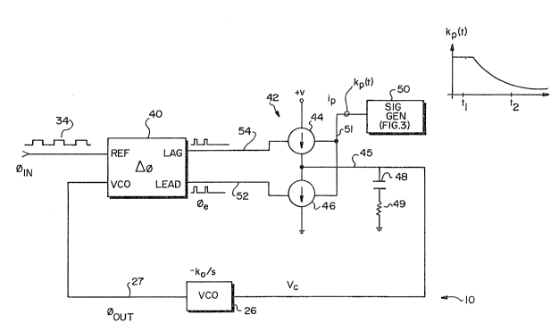
Fig. 2 is a high-level circuit diagram of one embodiment
of the PLL 10 according to this invention. This implementation
uses a lead-lag type phase comparator 40 to compare the
difference between the phase of the preamble portion 34 and the
VCO output 27 from the VCO 26. The means for adjusting the loop
response time is provided by a charge pump 42, which corresponds
to the variable gain amplifier 24 and a fixed loop filter 22 of
-- 11 --
1 3 1 07~6
PD88-0336/.5311-276
Fig. 1. The char~e pump 42 consists of a positive charge sourco
44, a negative charge source 46, a capacitor 48, and a discharge
control resistor 49. The amount of charge provided by positive
charge source 44 or negative charge source 46 to the capacitor 48
is controlled by a signal from the control signal generator 50,
in addition to the normal control via its input commands 52 and
54. One embodiment of generator 50 is shown in greater detail in
Fi~. 3, which is discussed later.
Still referring to Fig. 2, but more particularly no~, the
phase comparator 40 provides either lag or lead output pulses
depending upon whether the transitions of the VCO output 27
occur before or after transitions of the preamble 34,
respectively. The lag pulses are provided on a lag output 54
line, and the lead pulses on a lead output 52 line. The width of
the lead and lag pulses so provided is proportional to the time
difference between the pulse edges.
If lead pulses exist at the lead output 52, this indicates
the VCO 26 is phase-leadin~, and that its input voltage must be
decreased . Accordingly, then, the lead output 52 is fed to
control the operation of the negative charge source 46. The
negative charge source 46 then sinks a current on a charge pump
output line 45 to decrease the charge on the capacitor 48 through
the discharge control resistor 49. The amount of current sunk
by negative charge source 46 is directly proportional to both the
- 12
13107~6
PD88-0336/15311-276
width of the pulses received on lead output 52 as well as the
value of a response control signal 51, kp(t), output from the
response control signal generator 50. In accordance with this
invention, the response control signal generator 50 provides a
response control signal 51 which monotonically decreases from
time tl to a point after time t2 ~
Likewise, any lag pulses present at the lag output 54
control the operation of the positive charge source 44. The
positive charge source 44 thus sources a current directly
proportional to the width of the pulses on the lag output 54 as
well as the value of the response control signal 51. The
capacitor 48 is thereby allowed to charge.
An s-plane transfer function can be developed for the
circuit of Fig. 2, which in turn quantifies the effect of the
changes in gain of the charge pump 42 caused by varying the
response control signal 51 in terms of the Wn of the loop. In
the following analysis, symbols are assigned to the various
parameters:
kp instantaneous gain of charge pump 42
ip instantaneous current from charge pump 42
ko /s transfer function of VCO 26
~in input signal 34
~e phase error output of detector 40
~ 13
1 3 1 0746
PD88-0336/15311-2~6
~out VC0 output 27
Vc voltage input to VC0 26
c capacitance of 48
rl resistance of control resistor 49 times
thP capacitance of capacitor 48
a damping factor of the loop
Since the transfer function fo~ the charge pump is
ip = ~e kp
then from linear system theory,
1 ~ rl s
Vc = ~e kp
c s
and the loop function will be described by
~out (kp ko / c) ( 1 ~ 71 s)
=
.. . . . ~ .... .
, ~ ~in s2 + (kp k~ / c) 71 s + (kp ko / c)
1~ ~
1 31 07~6
PD88-0336/15311-276
which is recognizable as a standard ~orm transfer function of a
second order systems having an
Wn = i ( kp ko / ~ )
and
~ = Wn rl / 2
In the circuit of Fig. 2, the resulting change in natural
frequency, wnl is proportional to the change in the square
root of the value of the respohse control signal 51, kp(t).
Thus, the change in response time of the loop is inversely
related to the change in the square root of the value of the
response control signal.
Finally, a curve 56 of kp(t) versus time is also shown.
As previously mentioned, the gain of the charge pump 42 (i.e.,
the control on the loop response time) may be changed in any
suitably monotonically decreasing fashion. An exponential
change, as shown in curve 56, is optimum in the sense that the
largest changes in loop bandwidth occur nearest the beginning of
the preamble portion 34 of the loop input signal 12 (Fig. 1),
"~ - 15
1 3 1 Q7~6
PD88-0336/15311-276
when the loop bandwidth is greatest, and when the most time is
available to accomplish phasa lock. This can also be seen by
considering that the rate of change of the exponentlal gain
control ~unction in the curve 56 is lower nearest the ènd of
the preamble, at time t2~ when the loop is most vulnerable to
being upset by large changes in gain. Thus, while the bandwidth
has bacome very small, any adverse affect of changes in bandwidth
has been minimized, since the bandwidth is changing ever so
slowly by time t2. As will be secn also in connection with Fig.
4C, when the changes in gain have become sufficiently small near
time t2, the gain adjustment period is extended beyond the end
of the preamble portion 34 into the data portion 36. This
enables the use of a shorter preamble portion 34.
Fig. 3 is a detailed circuit diagram of an integrated
circuit implementation for the ~esponse control signal generator
50. The circuit operates with two supply voltages, V5 and vag,
to provide a ramping signal kp(t) having a maximum value vgo
(refer to plot 38 of Fig. l) and linearly decreasing to the
value vend between times t1 and t2. (The value vend
corresponds to vag minus v5c~ the Schottky voltage of the
transistor junctions in the circuit of Fig. 3~. The time t1 is
indicated to the circuit 50 by the rising edge of a pulse on an
input signal, HIL0. This pulse can be generated by any suitable
circuit, known in the art, which produces a pulse sometime after
the beginning the preamble 36. For the component values shown in
~,
16
1 3 1 07~6
PD88-0335/15311 276
Fig. 3, Vgo=1.25V, vag=5vl and vS-10v.
In the following discussion of the operation of the signal
generator 50, the dimensionless numbers written sideways adjacent
connecting lines indicate constant current in microamps. .
Now more particularly, the circuit 50 is separable into two
portions, a constant current generator portion, which produces a
constant reference current, is, at the collector of transistor
Q84, and a ramp generator portion , which produces a linearly
decreasing ramp current, if, at the collectors of Q81. The
output signal, kp~t), is thus the sum o~ the currents provided by
Q81 and Q84.
The reference current iS is primarily set by Q96, Q97 and
~98, and an external resistor rs connected to the integrated
circuit at an input/output pad K2. The multiple transistor Q96-
Q98 serves to sufficiently drive the load presented at the
output 51 by the charge pump 44 ~Fig. 2). In the illustrated
clrcuit oP Fig. 3, the reference current is equals five times
the ratio vgO/rs. The referPnce current is is mirrored throu~h
QR4 to the output 51. The other transistors Q90, Q94, and Q101
insure that Q84 is biased properly in the ON state.
The ramp current if is generated by rest of the circuit 50.
Its peak value is set by Vgo and an external resistor rf coupled
- 17 - ~
1 3 1 0-/ ~ 6
P~8-0336J15311-276
between the pad Kl and ground. In the embodiment depicted, the
peak if is equal to five time the ratio vgO/rf. The starting
time o~ the ramp i5 set by the state of a monostable flip flop
comprised of Q64 and Q65 and the associated constant current
sources Q6~, Q61, Q62, Q63 and Q67. This flip flop is set, if
Q65 is off upon receiving a rising edge at the HILO input coupled
to the bases of Q64 and Q65.
An external timing capacitor, ce, and a discharge current
source Q86-Q89, determine the duration of the ramp. The ratio of
the duration of intervals tl and t2 is set by R59. With the
component values shown, tl is set aqual to one-half t2.
In operation, when the flip flop transistors Q64 and Q65
are in the quiecent state awaiting a rising edge on the HILO
input (the time t=0 in the plot 38 of Fig. 1), Q65 is off. This
allows Q69 to turn on. As Q69 is coupled to control the base of
Q83, Q83 is in turn allowed to turn completely off thereby
raising if to its peak value. At this time, Q70 is off so that
the base voltage of Q77 is allowed to rise. A current (0:5 vgo /
R60) is mirrored through Q73 to develop a voltage equal to vgo
across R59. The voltage at ths pad CT is thus raised to 2v~o.
The edge of the pulse on HILO switches Q77 off, releasing Q83 so
that it can rise to a peak voltage value. The voltage follower
circuit formed from Q78 and Q79 then causes the voltage at the rf
pad kl to follow the lower of the voltage on capacitor ce and
- 18
- 1 3 1 07~6 69904-151
vgo. Thus, between time t=O and t=t1 the voltage at pad ct decays
to zero. Between the interval t=t1 and t=t2, it decays to zero
together with the ramp voltage. When time t2 is reached, the ramp
voltage at Q83 drops lower than vsc, causing Q66 to reset the
transistors Q64 and Q65 and to return the circuit to its initial
state.
Figs. 4A through 4C depict the results of simulations
performed with computer models of a conventional phase locked loop
and a phased locked loop constructed in accordance with the inven-
tion. They show how the invention is less susceptible to perturb-
ation that previous devices. Fig. 4A plots waveforms of a prior
phase locked loop circuit on a normalized time versus amplitude
scale. Fig. 4A includes plots of a loop input signal lOOa, a loop
gain control signal lOOb, and the resulting loop output signal
lOOc when the loop gain is abruptly changed at some point, t2,
after the loop has locked to an input preamble. Such gain control
signals having abrupt changes have been used with certain prior
circuits. Referring also briefly to Fig. 1, the signal lOOa
represents the phase of the input of the PLL lO (referred to as
~in in the above calculations), the signal lOOb represents the
gain control output 51 of the signal generator 50, and the signal
lOOc the phase of the output 27 of VCO ~6. A noise perturbation
105 was added to the loop input signal lOOa just before time t2.
Note the large phase error transient 110 caused by this perturb-
ation. The transient llO is approximately
19
X
1~107~
PD88-0336/15311-276
twenty-two time units long and 0.5 amplitude units in magnitude.
Fig. 4B shows another loop input signal 120a, gain control
signal 120b, and a loop output signal 120c associated with
another prior art PLL 10 . The loop input signal 120a was kept
identical to the previous input lOOa, with a corresponding
perturbation 125 linearly decreasing to time t2. However,
signal 120b has a ramp portion 121b in which it decreases
linearly until time t2, rather than an abrupt change as does
gain control signal lOOb. oscillations in loop error signal
120c caused as a result of the perturbation 125 are still
clearly visible. Thus, by ramping the bandwidth decrease in the
manner shown, the loop takes only approximately 17 time units, or
almost twenty-five percent less time, to settle out. The
amplitude has been reduced to 0.1 magnitude units, or about five
times better. However, a gain transient still occurs at time k2,
just when the data portion is about to begin.
Fig. 4C illustrates a similar plot from which is
discernible the advantages of this invention relating to the
change in loop bandwidth itself. Plotted there are a family of
gain control signals, 140a-140d, where the slope of the ramp
portion 142 is varied, together with the corresponding loop phase
error signals 145a-145d. As the slope of the ramp portion 142 is
decreased (compare 140a with 140c), the resulting responses
(compare 145a to 145c) "ring" less that is, the resulking
- 20
1 31 07~6
PD88-0336/15311~6
response is better damped. The traces 140d and 145d show the
result of extending the ramp past the time t2, ihto the data
portion 36 of the loop input signal 12. The loop reaches its
steady state at an even earlier time when this is done. Note
particularly that in the situation shown with response signal
145d , the loop has settled after about 10 time units. In every
other case, the loop requires additional time to settle. Thus,
if the ramp function is so extended, the preamble portio~ 34 can
be shortened even further, thereby shortening the time to phase
lock the P~.L 10.
The foregoing description has been limited to a specific
embodimant of this invention. It will be apparent, however, that
variations and modifications may be made to the invention, with
the attainment of some or all of the advantages of the invention.
FOr example, the present invention has been described as
particularly useful for acquiring data from a disk drive.
~owever, other data processing peripherals or systems needing in
general to acquire a digital signal in minimum time may make use
of the invention to their advantage. Therefore, it is the object
of the appended claims to cover all such variations and
modifications as come within the true spirit and scope of the
invention.
- 21