Note: Descriptions are shown in the official language in which they were submitted.
131~758
METHOI) AND APPARATUS FOR
ENCOD I NG AND TRANSMI TT I NG S I GNALS
The present invention relates to a system for encoding
and transmitting si~nals and, to the pLovision of a cable system
suitable ~o~ transferring the information in a plurality of
parallel signals from one set of conductors ~o a corres~onding
1~ remote set of conductors.
There are a variety of instances in which in-
~o~mation available in parallel form is to be transmitted
throu~ll a common channel in serial digital form~ Such
a serial signal may be generated by a parallel-to-serial
converter wllich sequentially and repetitively addresses
or samples a set of parallel signals to derive successive
pulses haviny values corresponding to the corresponding
contemporaneous values of the several parallel signals.
At the other end of the channel, the samples may be passed
through a serial-to-parallel demultiplexer which recon-
stitutes the original paLallel signals from the t~ans-
mitted samples. In an especially important form of such
systems the parallel signals are binary digital signals
h~ving at various times either one of two values or levels,
commonly designated as a O or a 1.
It is usual in such apparatus to sample all
o~ the parallel signals periodically and at the same rate,
suE~iciently oten that no significant changes occur in
an~ oE the parallel signals which are not detected and
represented by the samples. In such usual types of system
then, each parallel signal is sampled at intervals no
1 3 1 ~75~
-- 2 --
greater than the shortest time duration of significant
changes in any of the parallel signals. This requirement
~or sampling all of the signals at a specified minimum
rate requires a corresponding minimum bandwidth for the
transmission channel, in order to assure accurate and
reliable signal transmission over substantial distances.
The greater the required bandwidth, the shorter and/or
more expensive is the transmission channel which will
transmit the signals accurately and reliably.
a
It is an object of this invention to provide
a new and use~ul system and method ~or t.ansmitting in-
formation, particularly binary digital information.
Another object is to provide such system and
method which are conservative of the channel bandwidth
required to transmit the signals accurately and reliably.
Here described is such system and
2d method which, at least ~or parallel signals having certain
characteristics, accomplishes parallel-to-serial conver-
sion, transmission of the serial signals, and reconsti-
tution o the transmitted serial signals into parallel
signals, with a required bandwidth smaller than is nec-
essary in`conventional systems.
1 3 1 075~
In this disciosure, the original parallel
signàls are classified into at least two groups
a~co~dinq to the shortest time for whi~h they may stay
at a given level, the faster-changing group being desig-
nated herein as high-priority (HP) signals and the more
slowly changing group being designated herein as low-
priority lLP) signals. The LP signals are repetitiYely
sampled at a rate sufficient to provide accurate and
reliable transmission of them, and the resultant samples
1~ are applied to the transmission channel in serial orm,
except when a change occurs in any of the HP signals.
Such change in any one of the group of HP signals is de-
t~cted, the transmission of lower-priority signals im-
mediately terminated, and the HP signals immediately
sampled and transmitted through the common channel in
serial form, in place of the LP signals which would other-
wise be transmitted at that time. Preferably samples
of the entire group of higber-priority signals are trans-
mitted at such times. In the preferred embodiment, im~
mediately following ~he end o~ the higher-priority trans-
mission the sampling and transmission of the lower-priority
signals is resumed substantially where it le~t off.
1 3 1 075~
In this way the higher~priority signals are
sampled and "put through" the transmission channel im-
mediately upon a change in any of them, and the inter-
rupted lower-priority signal transmission is thereafter
S promptly co~npleted, ratheL than starting again at the
beginning of the low-priority sampling cycle. The result
is that the HP signals do not have to wait for the LP
signals to be sampled before re~eiving attention from
the sampler, and even with a relatively low sampling rate
any changed level of the high-priority signals will be
sampled befoLe it can disappear. The system is therefore
able to provides accurate and reliable information trans-
mission with a transmission bandwidth less than would
othe~wise be necessary~
1~ To permit proper use of the higher-priority
~HP~ and lower-priority (LP) signal samples at the other
end of the transmission channel, each group or "frame"
~orresponding to one complete sampling of the LP parallel
signals, or of the HP parallel signals, is preferably
~d identi~ied as being an LP or an HP frame by means of
identifying signals which are also transmitted through
the channel. PreEerably each of these identifying signals
c~mprises a pulse of a first given duration preceding
each LP Erame and a pulse of a second, shorter duration
preceding each HP frame. This enables the receiving ap-
paratus at the far end of the channel to recognize whether
an LP or an IIP frame is being received, so it can process
th~ two types of frames properly and deliver the trans-
~itted samples to the appropriate storage locations for
3~ r~constituting the original parallel signals.
Further as to the preferred embodiment, the
system at the input end of the transmission channel pre-
ferably comprises electronic switch means which in a Eirst
.
1 3 1 075~
position normally causes LP signals to be suppli~d to the
transmission channel bu~ which is responsive to a change in
any of said HP signals to be switched to its alternate
position, in which it causes the HP signals to be supplied
to the transmission line in place of the LP signals.
Preferably this is accomplished by means of a sampling
system which samples the parallel LP signals in a
predetermined order, which is interrupted in response to a
change in the HP signals but "remembers" where it leaves off
in sampling the LP signals, which next samples each of the
HP signals, and which then resumes sampling of the LP
signals, unless a further change in the Hp signal occurs in
which case it samples the HP signals again.
In accordance with a first aspect of the
invention, there is provided a priority system for
transmitting alternately, through a common transmission
channel, irst information contained in a first set of
signals variable at a relatively lower rate and second
information contained in a second set of signals variable at
a relatively higher rate, comprising:
first means for transmitting said first
information thxough said channel:
means responsive to the occurrence of
~5 predetermined types of changas in said second signals for
producing change-indicating signals;
means responsive to said change-indicating signals
for interrupting said transmitting of said first information
to transmit said second information through said channel; and
means for resuming transmission of said first
information upon completion of said transmitting of said
second information.
In accordance with a second aspect of the
invention there is provided, in a communication system
comprising a communications line, a first source of a first
set of N relatively more slowly variahle separate signals, a
second source of a second set of M relatively more rapidly
1 31 075~
- 5a -
variable separate signals, first means for repetitively
sampling said first set of signals successively to produce a
first set of corresponding sequential samples thereof on
said line, and second means for repetitively sampling said
second set of signals successively to produce a second set
of corresponding sequential samples thereof on said line,
the improvement comprising:
means for normally rendering operative said first
sampling means to produce on said line said first set of0 corresponding sequential samples;
means responsive to a change in any of said second
set of signals for interrupting the operation of said first
sampling means and for rendering said second sampling means
operative to produce said second set of corresponding
sequential samples on said line only in response to said
change; and
means for restoring the operation of said first
sampling means when said second sampling means has operated
to sample all of said signals of said second set a
?O predetermined number of times without a further change
occurring in any of said second set of signals.
In accordance with a third aspect of the invention
t~ere is provided, a system for transmitting information
~5 contained in a plurality of separate original parallel
signals, a first group of which signals are relatively
~lowly variable in value and a second group of which are
~ala~ively rapidly variable in value, comprising:
first controllably activatable sampling means for
~0 cyclically sampling said first group of original parallel
signals in sequence to produce a first series of samples
thereof at the output terminals;
second controllably activatable sampling means for
cyclically sampling said second group of original parallel
3~ signals in sequence to produce a second series of samples
thereof at its output terminals;
encoding means responsive to either of said first
and second series of samples for producing an alternating
- 5b - 1 3 1 075~
signal having two different values between which it
alternates substantially instantaneously, said successive
alternating values having time durations representative of
the corresponding values of said samples suppliQd thereto;
means for supplying said first and second series
of samples to said encoding means;
means for sensing predetermined changes in any of
said second group o~ original parallel signals to produce a
control signal indicative of the occurrence of any such
predeterminad change;
means responsive to said control signal for
normally activating said first sampling means, and for
activating sai~ second sampling means and deactivating said
first sampling means immediately upon the occurrence of one
of said predetermined changes;
means operativa upon the completion of said
sampling of each of said second group of original parallel
signals for deactivating said second sampling means and
activating said first sampling means at the point in its
cycle where it was last deactivated;
a signal transmission channel; and
means for applying said alternating signal from
said encoder means to said transmission channel.
2S En~odiments of the invention will now be described
with reference to the accompanying drawings, wherein:
Figure 1 is a block diagram illustrating one use
of the invention;
Figure 2 is a perspective view, with parts broken
away, of a cable system embodying the invention in a
presently-preferred ~orm;
Figure 2A is an enlarged, fragmentary perspective
view showing the constxuction of one of the types of cables
shown in Figure 2;
Figure 2B is a similar view of the other type of
cable shown in Figure 2;
1 3~ 075~
Figure 3 is a block diagram of the electrical
system used in the connector plug assemblies of Fi~ure
2;
Figures 4-7 are graphical representations, to
a common hori~ontal time scale, to which reference will
be made in e~plaining the nature and certain advantages
o~ the encoding system~f the present invention;
.~
Figure 8 is a block diagram of the electronic
circuitry preferably employed in both of the cable con-
nector plug assemblies to achieve parallel-to-serial con-
version;
Figure 9 is a block diagram of the electronic
circuitry preferably employed in both of the cable con-
nector plug assemblies to achieve serial-to-parallel con-
version;
Figures 10 and 11 are graphical representationsshowing waveforms with reference to which the typical
nature of the information conveyed by the system will
be described;
~0 Figures 12 and 13 are graphical representations
o~ various signals occurring in the MUX and DEMUX units
oE a preferred embodiment of the invention, respectively;
Figure 14 is a functional block diagram of a
p~ferred form of input transition timer for use in the
r~oeiving portions of each cable connector plug assembly;
and
Figure 15 is a series of timing diagrams or
graphs, to the same time scale, illustrating the operation
of the timer of Figure 14.
~ `
1 3 1 075~
DETAILED DESCRIPTION OF SPECIFIC EMBODIMENTS
-
Referring to the speciEic embodiments o the
invention shown in the figures by way of example only,
and without thereby in any way limiting the scope of the
S invention, Figure 1 illustrates one communication system
to whLch the invention is applicable. Here there is shown
a data center 10 at which there is located a computer
CPU 12 having front end processors FEP-l, FEP-2 and FEP~
3. Such front-end processors typically have from 16 to
la ~ or more ports to which modem cables may be connected.
T~e p~l~pose o the front-end processors is to relieve
tlle host computer of the processing burden uniquely as-
~o~i-ated with maintaining communications between elements
a~ a data communications processor. The F~P~s 1, 2 and
1~ 3 are provided with respective FEP female connector plug
units 16, 18 and 20 mounted thereon, each containing multi-
ple Eemale connector members presenting parallel signals
~or transmission to associated modems (for example, MODEM
1, ~SODE~l 2 and MODEM 3, respectively), and also having
_d Eemale connector members for receiving signals delivered
to ~hem ~rom such modems. In a typical example, connect-
o~ plu~ units 16, 18 and 20 and each of the other inter-
unit connector plug units may have 25 connector members,
in the EI~ 'ry~e RS-232-C connector. Male connector
plug units 21, 22 and 23 contain connector members mating
h tl~ ~emale connector members of plug units 16, 18 and
2~ ~apectively~
Communication lines 24, 26 and 28, commonly
re~e~ed to as data set cables, connect male connector
3a plu~ units 21, 22 and 23 to male modem connector plug
units 29, 30 and 31 which in turn are matable with cor
responding female connector plug units 32, 33 and 34 mounted
- 8 - 13~ 015~'
on respective modems 1, 2 and 3 to permit two-way transmis-
sion of signals between the FEP's and the modems. The
other ends of the modems are operatively connected to
the adjacent ends of telephone company lines 36~ 38 and
40 by conventional connectors, rot shown.
More remote from the data center 10 is an office
38 containing, in this example, remote terminal 1, remote
terminal 2 and remote terminal 3, which may be word pro-
cessors, financial accounting computers, personal com-
puters, etc. In this instance it is desired to connectthe remote terminals for two-way communication with the
CPU 12 by way of the telephone company lines 36, 3% and
40 r the modems 1, 2 and 3 and the FEP's 1, 2 and 3 at
the data center. This is accomplished by means of the
modems lAr 2A and 3A at the officer and the data set cables
50 r 52 and 54 provided at one of their ends with connector
plug units 56, 58 and 60 and at their other ends with
connector pluy units 62r 64 and 66r respectivelyr for
plug-in connection with corresponding connector plug units
on the modems lA 2A and 3~ and on remote terminals 1-3.
It will be understood that each of the modems
shown may be at a substantial distance from its corres-
ponding FEP or remote terminalr e.g. 100 to lrO00 feet.
This is primarily because the modems are usually located
where the telephone company lines enter the building,
which is normally at a substantial distance from the com-
puter CPU and the remote terminals
Further, it will be understood that usually,
and in this exampler the FEP's, modems and remote term-
inals ar~ designed to accept and utilize parallel digitalsignals presented to them on the various connectors shown,
9 13107~
which signals typically consist of data and clock pulses
together with a substantial number of control and signal-
ling pulses for establishing proper contact, lock-in and
other functions.
In Figure 1 the data set cables and the connector
plug units at each of their ends are shown only schematical-
ly, and in a prior-art system each such cable would com-
prise one conductor for each of the operative pins on
tlle connectors. In the present example, this could in-
volve a 25-conductor cable, if all pins are used; such
cabl~s are expensive, as well as bulky and difficult to
place and dress in a convenient, unobtrusive manner.
In one o~ its aspects, the present invention replaces
such a multi-conductor cable with a much simpler commu-
nication line, for example a cabling containing over mostof its length only two twisted-pairs of wire, one pair
transmitting serial signals in one direction and the other
pair transmitting serial signals in the other direction.
To enable this operation, each of the connector plug as-
semblies secu~ed to the opposite ends of each data set
~able sucll as 24 preferably includes both a serial-to-
parallel and a parallel-to-serial converter, whereby par-
allel signals travelling in either direction will be placed
upon the data set cable in serial form, and at the op-
posite ~nd of the line will be converted back to parallel.
Since all o~ the cables and connector plug as-
semblies may be the same, only data set cable 24 and its
connector assemblies will be described in detail. Phys-
ically, the form of cable assembly of the invention which
is shown in Figures 2, 2A and 2B is suitable for use be-
tween each of the modems of Fig. 1 and its associated
FEP or remote terminal, and in this example it will be
-- 10 --
1 3 1 075~
assumed that ~t is used for all modem connections. Nu-
merals used in Figure 2 which correspond to those used
in Figure 1 denote corresponding parts.
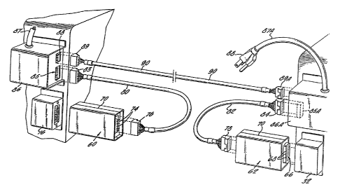
Referring then to Figs. 2, 2A and 2B, in this
example tlle cable connector system comprises two iden-
tical converter plug units 60 and 62, each comprising
a connector pin portion such as 66 provided with a set
of ~5 male connector pins such as 68 mounted at one end
o~ a generally rectangular metal or plastic plug housing
1~ 70 and adapted to plug into the connector plug units 16
and 32 on the FEP-l and Modem-l. At the other ends of
~ach of the units 60 and 62 is provided a set of 7 male
connector members such as 74, adapted to mate with the
c~rresponding 7 female connector ~embers of female plugs
1~ 7~ and 78 respectively. The plugs 76 and 78 are connect-
ed to 7-wire cables 80 and 82 respectively, shown in Fig.
2B, which are typically only a few feet long and provided
at their other ends with seven-pin female plugs 83 and
84, respectively. These plugs are adapted to mate with
male plug UllitS 85 and 85~ mounted on dc power supply
uni~s 86, ~6~ Lespectively. The latter power supply units
ar~ mounted adjacent the respective plug units 16 and
3~. The power supply units are provided with ac line
cord~ 87 and 87~ terminating in ordinary ac wall plugs
S ~uc]l as ~8 for plugging into corresponding ac power-line
~o~k~ts adjacent the e~uipment. Each of the power supply
unit~ contains a small ac power supply, with appropriate
~c~iEying and filtering elements, for providing a rela-
~iv~ly low dc voltage, for example 18 volts isolated from
3d g~ound, to t'ne converter plug units 60 and 62, wherein itmay be adjusted to +9 and -9 volts.
1 3 1 075~
Also provided on the power supply units are
5-pin male connector plugs such as 88, matable with female
5-pin plugs 89,89A on the opposite ends of 4-wire cable
90. The latter cable contains the two twisted-pair lines,
as shown in Figure 2A, which carry the serial multiplex-
ed signals. A ground wire may optionally be included,
and if used may be in the form of an outside cable shield.
It is these two twisted-pair lines which are typically
of substantial length, e.g. up to 1,000 feet, and present
very substantial advantages in reduced expense and size
as compared with multi-conductor lines of perhaps 25 con-
ductors of the same length previously used for the same
~eneral purpose. Furthermore, such twisted-pair lines
are o~ten already in place in ~ ~uildings, having been
previously used ~or other purposes, or installed for pos-
sible future use, and use of such existing lines for cable
90 will generally provide a substantial financial saving.
In some cases a single twisted-pair line may be used be-
tween the connectocs of the connector plug assemblies,
either when transmission is to be only in one direction
or when the system permits the line to be used alternately
for transmission in both directions. However, it is here
preferred to utilize a separate line for each direction
oÇ transmission, within a single cable, and the invention
~5 will be described with particular reference to such el~-
bodiment.
It will be understood that, in use, one merely
plugs each of the connector plu~s 89 and 89A at the op-
posite ends of the 4-wire cable 90 into the power supply
plug receptacles such as 88, plugs each of the 7-wire
cables into one of the power supply units and the associat-
ed converter plug unit 60 or 62, and plugs the two ac
line cords 87 and 87A into ac wall sockets adjacent each
power supply unit. Inside the power supply units the
- 12 -
1 3 1 075~
two twisted-pair lines of cable 90 are directly connected
to the two twisted-pair lines in each of cables 80 and
82, to complete the two twisted-pair line extending from
converter unit 60 to converter unit 62.
It will also be understood that in other embodi-
ments the dc power ~or each converter unit may be provided
completely independently of the signal ca~les, e.g. through
the plug unit 16, in which case the two twisted-pair lines
may extend directly ~rom converter plug 60 to converter
plug ~2, rather than by way oE the power supply units;
or a "free-standing" power supply unit may be used, sup-
ported only by the signal cable rather than being mounted
to a frame.
Figure 3 illustrates broadly the electrical
circuitry mounted within the case of each of the connector
plug assemblies 60 and 62 of the cable connector system.
For the present purposes it is assumed that the circuitry
shown is that in the connector plug housing 70 of con-
verter plug unit 60, which is plugged into connector plug
~d receptacle 16. However, the same type of unit would be
used in the converter plug unit 62 which is plugged into
connector 32 of MODEM 1, and in all of the other converter
plu~ units secured to all of the other cables shown in
Fi~ure 1.
In Fig. 3, it is assumed that the connector
pin assembly 66 has 25 pins, two of which are used for
data pulses and clock pulses to be delivered to Modem-
1 ~rom FEP-l, two of which are to receive data and clock
pulses from Modem-l, one of which provides a frame ground,
3~ one oE which provides a signal ground, two of which con-
stitute + and - voltage test points, and the remaining
16 of which are for inErequently-changing control signals,
used in both directions of transmission.
"~ `
- 13 - l 31 075~
Figures 10 and 11 show typical input signals
applied to converter plug units 60 and 62, to illustrate the
general magnitudes of the frequencies and time intervals
typically involved, in this case for half-duplax operation.
In Figure 10 the signals named at the left
originate at an FEP-l of the CPU, while those named at
the right originate at the MODEM 1. In Fig. 10A there
is shown a Data Terminal Ready signal, constituting a
high level produced by the terminal when it is in a ready
condition; this signal may persist all day, or for at
least minutes at a time. At lOB is shown a Data Set Ready
signal, originating at the MODEM, which also is typically
on for hours or at least minutes. Figure 10C shows a
Request To Send signal from the terminal end, consisting
here of two spaced-apart pulses each of a duration to
encompass a useful block of data; Figure 10~ shows two
corresponding Clear To Send pulse signals from the MODEN
end, only slightly delayed with respect to the Request To
Send signal, each pulse being of comparable duration to the
Request To Send pulses. As represented by the shaded area in
- 14 -
1 3 1 075~
Figure lOE, the terminal equipment has been sending clock
pulses continuously, at a high rate, as depicted in Fig.
llA, and a block o~ high-speed data is sent by the term-
inal during the pulsès shown in Fig. lOF, each such pulse
starting after a Clear to Send pulse and endin~ at the
end of the Request to Send Pulse; typical data are il-
lustrated in Figure llB.
Figure lOG shows the Carrier Detect signal orig-
inating at the Modem upon detection of data being sent
1~ from the remote Modem.
Figure lOH sho~s the Receive Clock signal orig-
inating at the Modem and derived from the data being sent
~rom the remote Modem.
Figure lQI shows the Receive Data signal orig-
inating at the Modem and resulting from demodulation ofthe siynal sent by the remote modem.
The binary data shown in Fig. 11B are in stand-
ard NR2 form and, during each associated clock pulse of
Fig. llA, represent the series of l's and O's at the bot-
tom of Fig. llB. This is the data contained in the en-
velope oE the signals of Fig. 10 indicated by diagonal
lines.
The clock pulses of Fig. llA define a clock
rate, which is also the data bit rate, and which may typ-
icall~ be anywhere from about 2,400 to 19,200 bits per
second; thus a bit time may be as short as about 52 micro-
seconds. Message lengths (data blocks of Fig. lOF) may
vary from about 10 to 2,000 eight--bit characters, i.e.
from 80 to about 16,000 bits. Assuming operation at the
high-speed end of this ranges, a message of 16,000 bits
.,~ .
j
1 3 1 075~
may be sent in a block having a duration of about 0.832
secollds, with each bit time having a duration of about
5~ m;croseconds. The clock pulses, however, are then
considerably shorter in duration than the bit interval,
e.g. about half as long, or a~out 2~ microseconds long
with 26 microseconds between them. In order for the clock
pulses from a terminal or CPU to be sampled and trans-
mitted properly by the sampling systems of the multiplexers
used in tihe present invention, and with the sampling oc-
l~ curring s~nchronously with respect to the clock pulses
~ ~or example an 8 KHz rate 1125 microseconds per cycle
o~ sampling of each of the 12 signals), it is desirable
t~ resample each input signal at leas~ twice per system
clock cycle, e.g. at least every 26 microseconds; this
would merely assure sampling at least at the edges of
a clock pulse, and to provide sampling which will assure
accurate sensing of when each clock pulse starts and ends
(the timing of its edges), at least several samplings per
half clock cycle are needed. In fact, the position oE
a clock pulse edge, or of a data signal. transition, can
anly be detected with a time tolerance about equal to
hal~ the time interval at which it is resampled. Accord-
ingly, i~ one wishes to represent the position of an edge
o~ a ~6 microseconds clock pulse with an accuracy oE 6
m~roseconds one should sample at least every 6 micro-
~conds witll a very narrow sampling interval (fractions
~icrosecond).
~ s will presently be described, each of the
~3r~ 3lowly or in~requently variable signals tiOe. all
33 ~ce~t t~e clock end data signals) is generally sampled
at a relatively lower rate (at 8 to 14 microsecond in-
tervals, depending on the values of the input signals
being sampled), and each of the more rapidly variable
- 16 -
1 3 1 075~
signals (the data and clock signals) is generally trans-
mitted with a shorter waiting-time (3.~ to 5.5 microsec-
on~s, depending on tlle values of the signals being sam-
pled).
Referring now to Figure 3, amplifiers 92 and
94 supply the separate parallel high-priority and low-
priority signals, respectively, from plug 66 to a parallel-
to-serial multiplexer 96, preferably provided on a semi-
conductor chip 97 physically located within the plug hous-
10 ing 70 of Fig. 2. The output of the multiplexer 96 is
supplied through balanced-output driver amplifier 98 to
twisted-pair wires 100. The latter twisted pair extends
physically through cable 80, power supply units 86 and
~6A and cable 90 of Fig. 2, to Modem-l. DC power from the
1~ power supply unit 86 is supplied over the two lines
101 .
Conversely, serial digital information arriving
~rom Modem-l on twisted-pair wires 120 in cable 80 passes
through the balanced-input receiver ampli~iers 122, and
~0 the output of the latter amplifier is supplied to the
serial-to-parallel demultiplexer 130 on chip 97. The
reconstituted parallel HP information is supplied ~rom
demultiplexer 130 through amplifier 132 to appropriate
pins of the connector plug 66, while the reconstituted
~5 parallel LP information from the demultiplexer is supplied
by way of amplifier 134 to other appropriate pins of the
sflme connector plug. It will be understood that each
oE the amplifier components 92, 94, 132 and 134 designated
"~" actually includes a plurality of amplifier devicesr
3n as appropriate for their respective functions. Prefer-
ably, a timing oscillator 140 is also provided on chip
97, the crystal stabilizing unit 142 for which is con-
nected to the oscillator circuit on the chip but is mount-
ed separately from the chip within the plug housing.
-- 17 --
131075~
Figure 4 shows tlle pulse du~ations which are
utili~ed in this embodiment to represent in serial Eorm
on twisted-pair wires 100 the parallel information pre-
sellted at connector plug 16 of FEP-l. As indicated at
A in Fi~. 4, a binary 1 is represented by two identical
but oppositely poled 0.5 microsecond pulses, one on each
of the wires of the twisted pair 100; as shown at B, a
binary O is represented by two oppositely-poled 1 micro-
second pulses; as represented at C, the "IIP sync" pulse
which identifies high-priority data is represented by
two oppositely-poled 1.5 microsecond pulses; and the "LP
sync" pulse which identifies LP data is represented by
oppositely-poled pulses 2 microseconds in duration, in
this example.
lS Fi~ure 5 illustrates a low-priority frame formed
~y the multiplexer 96, and Figure 6 illustrates a high-
priority ~rame formed by that multiplexer. Referring
to Fig. 5, the 2 microsecond initial pulse labelled "LP
Sync" represents the pulse on the two-wire line which
~ identifies the immediately subsequent data pulses as re~
lating to an LP frame. The pulses labelled 1 through
12 represent, by their individual durations, the arbi-
trarily chosen binary levels of a group of 12 original
parallel LP signals supplied to the input of the multi-
~5 ple~er, specifically in this example 110010111011. TheErame is then repeated, with numbers of O's and l's ap-
propriate to the values of the original parallel low-prior-
ity si~nals at that later time. The terminal hal~-micro-
s~cond portion o~ the LP s~nc pulse is cross-hatched to
~ndicate a ~ime interval near the end of the LP sync pulse
durin~ which the LP ~rame cannot be interrupted by an
IIP Erame, ~or reasons described more fully hereinafter.
Unused pins tor pins with constant levels) are not con-
nected to the Mux at their source connector. At their
destination connector, corresponding pins are connected
A;
- 18 -
1310758
to either a ~ or - voltage from the cable multiplexer
power supply. Pins on the cable Mux chip corresponding
to unused bits within the multiplexed frame are tied to
a -~ voltage from the cable multiplexer power supply so
S tllat they are se~sed and transmitted as binary ones and
therefore require a shorter t~ansmission time.
Figure 6 shows the HP sync pulse of duration
1 microsecQnd followed by 4 data pulses each having a
duration which depends upon whether the pulse is repre~
la sentin~ a binary 1 or 0, in this example the ~rame is made
u~ o~ HP bits 1, 2, 3 and 4 is assumed to represent binary
digits 1, O, 1 and 0, respectively.
The yraphs of Figure 7 illustrate some of the
~dvantages of the above-described general type of pulse
1~ widtll encoding of information. At Fig. 7a there is shown
a previously-known NRZ encoding of the binary digital
in~ormation 110010111011. It utilizes 12 corresponding
time slots or bit intervals of equal durations - in this
e~a~ple about 1 microsecond; a corresponding 1 MHz clock
s;~3nal is shown at 7s. The bit rate is constant, and
each bit interval contains a level which is either Low
o~ T~igh ~epending upon whether a O or 1 is represented
The total time for transmission of this information is
therefore 12 microseconds.
2~ In Fig. 7C there is illustrated a known ratio~
codin~ system used to represent the same information.
In this ~ncodin9 system a 1 is represented within each
1 microqecond time slot by a High level which is longer
~han the Low level, while a O is represented by a Low
3~ level longer than the High level. Again, the bit rate
is constant and 12 microseconds are required for the frame.
. ~
-- 19 --
1 3 1 075~
At. Fig. 7D there is shown an encoding scheme ac-
cording to a preferred form of the invention, designated as
NR2D encoding, according to which each successive pulse be-
gins substantially immediately upon termination of tlle pre-
ceding pulse. Since in this example there are ~ binaryl's and 4 binary O's in the frame, there are 8 halE-micro-
second pulses and ~ one-microsecond pulse, the total time
required to represent the information therefore being
~ microseconds. If all of the bits had been l's, the
time to represent the information would be only 6 micro-
seconds, or one-half the time re~uired by the conventional
encoding systems of Figs. 7A and 7C. If all pulses had
been O's, rather than l's, the time required to represent
the information would be 12 microseconds, as in the prior-
art systems; if the information is random (half l's andhalf OISJ on the average), the average time required will
be 9 microseconds. In many systems it is known ahead
of time that either O's or l's will predominate, and by
representing the more frequently-occurring binary value
by the shorter pulse duration, the required time Eor a
co~plete representation of the data will always be less
than 8 microseconds, in the particular system under dis-
cussion.
Fig. 7E shows the same encoding scheme as in
~S Fig. 7D, but with the levels reversed in polarity. For
practical reasons it is preferred in the present embodi-
ment to ~use both of the waveforms of these two figures,
one on each of two twisted-pair wires, to give the dual
balanced waveform depicted in Fig. 5.
An important advantage of the reduction in frame
time provided by the invention is that where the pulses
of different durations represent successive values of
- 20 -
1 3 1 075~
a plurality of repetitively-sampled original signals,
the shorter frame time resulting from the invention means
that each of the original signals will be sampled more
frequently than otherwise - that is, the frame can be
~e~reshed more frequently, to give better representation
o~ the information.
Figures 5 and 7D also illustrate another aspect
of the preferred form of the invention, according to which
the successive encoded pulses are provided with alternating
polarities. The result of this is that the transmission band
required to send tlle encoded signals ~tith a given degree of
distortion is only about half that which would be required
~or the signals of Figures 7A or 7C, for example. Ac-
~o~dillgly, in the above example, a transmission channel
having a maximum modulation rate of 1 Mhz can transmit
a steady stream of zeros at a 1 mbps rate, where each
zero is represented by a 1 microsecond pulse and alternate
pulses are of opposite polarities. The same transmission
~hannel can transfer equally well a steady stream of one's,
~0 each represented by a half-microsecond pulse, with every
alternate pulse having an opposite polarity, at a 2 mbps
r~te. If the signal being transmitted averages half zeros
~n~ halE ones, its effective transmission rate will be
1.5 mbps, whicll can be passed through a channel having
~5 a maximum modulation rate of 1.0 mbps without appreciable
distortion. It has been found that in such a system of
the invention one can provide reliable operation over
about a 1000-foot length of good twisted-pair cable; if
~ lowe~ maximum modulation rate of say 500,000 is used,
30 good results can be obtained with a 3,000-4,000 foot cable.
It is noted that the encoding technique of the
preferred form of the invention as depicted in Fig. 7D, for
example, is also very easy to implement, since in essence
- 21 -
~ 3 ~ 075~3
one need only provide a waveform ~hich alternates between
two fixed levels, and maintain it at each level for either
one of two time intervals, depending upon whether the level
is repre~enting a 1 or a 0.
In the above discussion of Fig. 7, the efEects
of the LP and HP sync pulses have not been considered,
since they are not necessary in all embodiments oE the
novel encoding system; their main function is to differ-
entiate between HP and LP data whenr as in the preferred
embodiment, the input signals are classified and divided
into HP and hP signals and processed differently. In
other forms of the invention such classi~lcation and dif-
ferentiation need not be employedr and although some form
of synchronizing or timing may be desirable it can be
lS accomplished in very different ways. However, in the
preferred embodiment now being described, a complete LP
frame includes an LP sync pulse as shown in Fig. 5r and
a complete HP frame includes an ~P sync pulser thus adding
2 microseconds to the LP frame time and 1~5 microseconds
to the HP frame timer giving frame times for the examples
of Figs. S and 6 of from 8 to 14 microseconds for the
LP frame and from 3.5 to 5.5 microseconds for the HP frame.
Figures 8 and 9 show further details of the
preferred form of the multiplexer and demultiplexer sys-
tems depicted more generally in Figure 3.
Referring first to Figure 8r there are shown1 low-priority signal input lines 200 from the ampli-
Eiers 94 of Fig. 3r carrying the original, parallel, more-
slowly variable LP signals. These input lines are con-
~0 nected to the signal input terminals of a 12-input scanner
202. In response to successive addresses supplied thereto
over lines 204 from Mod-13 counter 206r the scanner 202
~ .
- 22 -~
1 3 1 075~
in effect connects successive ones of the input lines
momentarily to the single output line 208 of the scanner.
The sca~ er thus ope;ates as a repetitive sampler of the
12 input signals thereto. In addition, the first, thir-
teenth, twenty-fifth, etc. pulses from the Mod-13 counter
are applied directly over LP sync line 212 to the output
transition timer 214; these pulses constitute the timing
source for the generation of the "LP Sync" signal by the
output transition timer, which sync signal precedes and
1~ serves to identify tle immediately following group or
block oE pulses as LP signals.
In the absence of high-priority information
then, the LP input signals are sampled and the binary
1 and O samples passed serially through the normally-trans-
1~ missive NAND gate 220 and through OR gate 221 to the out-
put transition timer 214; the digital data on the signal
input line 213 of the transition timer are therefore in
serial form, the successive pulses thereof indicating
the co~responding levels of the parallel signals at the
2d input to the scanner.
The output transition timer 214 responds to
all oE its input signals to produce on its output line
~2 timing pulses which determine when transitions in
th~ stat~ of output toggle flip-flop 223 occur. 223 is
?5 ~ so-called D flip-flop whicb upon the occurrence of each
l~ading edge of a timing pulse on line 222 assumes at
its output line 224 a state (High or Low) opposite that
o~ its D input on line 225. Accordingly, the output of
~lip-flop 223 executes a transition between its High and
Low states each time a timing pulse on line 222 appears,
and the time for which it remains in either state depends
on the time between successive timing pulses. The output
on line 224 is therefore the desired NRZD signal.
- 23 -
1 3 1 075~
In the absence of changes in the HP signals,
the output transition timer 214 first produces on its
output line 222 a ~Liming pulse which initiates the Low-
Priority Sync pulse of 2 microseconds duration, followed
S by a timing pulse which terminates the sync pulse. The
ne~t timing pulse changes the state of the flip-flop 224
one-hal~ or 1 mic~osecond later, depending upon whether
a 1 or a 0 is to be represented.
The Mod-13 counter 206 is not free-running,
1~ but ollly advances its count to shift sampling to the next
inpu~ signal in response to a clock pulse delivered
~a i~s clock input terminal 226 over line 228 from ~ND
g-lt~ ~3d. One input terminal 232 of the latter gate is
sllpplied with ~dvance signals from output transition timer
214, over Advance line 236. These Advance pulses are
th~ same as the timing pulses on line 222, and are denoted
a5 Advance pulses to facilitate easy comprehension of
their Eunctions. Accordingly, each Advance pulse occurs
at a transition in the output NRZD signal, and serves
~a to sni~t the scanner to the next LP input signal, to pro-
duc~ a binary sample "telling" the output transition timer
whekher to wait 1 or 0.5 microseconds before producing
~h~ next timiny pulse. The other input to the AND gate
~3~ is supplied over output line 240 from the High-P~ior-
ity, Low-Priority Frame Flip-Flop (HP/LP FR FL') 242, which
in its normal state supplies to AND gate 230 a level which
r~nd~rs it transmissive and permits the Advance signals
~o pass through the AND gate 230 and to advance the Mod-
13 counter, during transmissions of LP siynals.
3~ Considering now the circuitry shown in Fig.
8 Eor accomplishing special handling of the HP signals,
the four high-priority information input lines 246 carry-
ing the parallel HP signals are supplied both to the sig-
nal input terminals of a conventional four-input scanner
- 24 -
131075~
250, operative when activated to sample the HP signals,
and to a conventional level-change detector 252 for sens-
ing when a change occurs in any of the four input signals.
Normally, during the transmission of low-priority siynals,
tlIe four-input scanner is not activated and produces no
output. However, when one of the four HP siynals cllanges
level, this change in level is detected by the level change
detector 252, which may be a device of known form ~hich,
in effect, merely stores the most recent levels of the
four signals and then compares each of them with its next
subsequent value to detect any changes therein. Upon
such detection of a change of level of any of the four
signals, the output of detector 252 changes to its op-
posite state. The latter change in level passes through
normally-transmissive NAND yate 260, the control term-
inal 262 of which is connected to an END OF LP S~NC line
266 which normally permits this to occur. ~he resultant
change in level at the Set input 270 of the EIP/LP FR FF
242 causes it to switch immediately to its opposite state,
~0 in which its output line 240, denoted LP FRAME, goes Low
and its other output line 272 (marked ~IP FRAME) goes High.
This change on line `240 makes AND gate 230 nonresponsive
to the Advance pulses so as to terminate the LP signal
sampling by scanner 202, and renders N~ND gate 220 non-
transmissive so that the output of scanner 202 is isolatedfrom the outp~t transition timer 214; at the same time,
the change on line 272 renders NAND gate 280 transmissive
oE the Advance pulses applied to it over line 236, and
the latter Advance pulses are thereby applied over line
281 to the Mod-5 counter 282 to operate it through one
cycle ~f ~ive counts and to step the scanner 250 through
its five positions, after which ~IP/LP FR FF 242 reverts
to its normal state and supplies a signal to the reset
terminal RST of level change detector 252 to reset it.
- 25 -
1 3 1 0-15~3
Accordingly, during the ~od-5 count, in response
to the ne~t Advance pulse, Mod-S counter 282 puts out
on line 283 a High-Priority Sync timing pulse for appli-
cation to output transition timer 214, which responds
r~ by hol~ing Eliy-Elop 223 in whatever state it is in for
1.5 microseoollds, to form the NRZD HP Sync pulse; at the
etl~ 0~ this sync pulse the next Advance pulse is applied
ov~r Advance line 2~6 through AND gate 280 to the Mod-
5 counter to produce the Eirst address signal in the 4-
input scanner 250 and thereby sample tne first HP input
signal. This sample passes through NAND gate 284 (nor-
mally non-transmissive, but rendered transmissive by the
~P FR~ME signal on line 272) and OR gate 221 to the output
transition timer 214, which causes the timer 214 to pro-
lS duce a half or a one microsecond pulse at the NRZD outputline 224 depending on the sample. At the end of this
output pulse, the next Advance pulse is generated and
advances the Mod-5 counter by one count and the input
scanner to its next address, analogously to the operation
~d oE Mod-13 counter.
In this way the inEormation on the Eour high-
priority input lines is encoded on the NRZD output line
~2~ in the Eorm o successive pulses of alternat;ng po-
larity, one immediately following the other~ and with
~ither half-microsecond or one-microsecond durations de-
~nding upon whether they are representing a 1 or a 0.
I~ no ~urther level chànge occurs in any oE the HP sig-
nal3, ~here i~ no Çurther output Erom the previously-reset
l~v~l chanqe detector 252, and the HP/LP FR FF reverts
33 to its normal state in response to the END OF HP FRAME
~ignal produced on line 290 by the end oE counting in
Nod-5 counter 282. In response to the reversion oE the
~P~LP FR FF 242 to its normal state, the Mod-13 counter
- 26 -
1 3 1 075~
resumes it~ counting at the point where it left off, thus
causing scanner 202 to complete its sampling of the r.P
~rame.
The above-mentioned END OF LP SYNC line 266
is normally supplied by the output transition timer 214
with a level which maintains the NAND gate 260 in its
transmissive condition. However, during the latter part
of each low-priority frame sync pulse, represented by
the shaded area in Fig. 5, the output transition timer
produces a level on line 266 which renders NAND gate 2~0
non-transmissive during such time. Accordingly, if a level
cllanye detector pulse occurs in this time interval the
LP scanner 202 will nevertheless continue to operate until
the end oE the LP sync pulse, at which time a change in
level on line 266 renders NAND gate 260 transmissive a-
gain, and the high-priority frame will begin. The dura-
tion of this period of non-interruptability of the LP
sampling is in this example about one-~alf microsecond,
so that the maximum time required to produce an HP sample
is increased in such event by a half microsecond, to a
~tal of Erom about 4 microseconds to about 6 microseconds.
It is noted that, with the exception of this
time interval near the end of the LP sync pulse, the high-
priority frame may inject itself into the low-priority
Erame at any time, even during the LP frame Sync Pulse
~nd even during one of the LP binary data-representing
pulses of one-half or one microsecond normal duration.
~his will be more fully appreciated ~rom the discussion
~reinafter of the timing diagrams of Figs. 10 and 11.
Internal clock timing for the multiplexer is
provided by a cloc~ oscillator 292.
1 3 ~ 075~
The NRZD output of output toggle flip-flop 223
in this example is passed through balanced driver 98 of
Figure 3 to the twisted-pair line 100, whereby two such
NRZD signals of respectively opposite polarities ar~ placed
on the two wires, as described previously.
A demultiplexer corresponding to the demulti-
plexer of Fig. 3, and usable with the multiplexer of Fig-
ure 8, is shown in Figure 9. In Figure 9 the double-ended
balanced pair o~ signals on line 120 of Fig. 3 have been
passed through the balanced receiver amplifier 122 of
Fig. 3 to NRZD input line 300, which conveys them to the
signal input of input transition timer 303, clocked in
response to timing provided by an asynchronous oscillator
301. Transition timer 303 senses the time o' occurrence
of each transition in the level of the received signal,
and measures the times between successive transitions.
After so doing, it applies a pulse to HP SYNC line 304
upon reception of a l.S microsecond pulse, applies a pulse
to LP SYNC line 306 upon reception of a 2 microsecond
pulse, applies a narrow pulse to transition clock line
308 whenever a data-representing transition in level occurs
in the received signal and, when data pulses are received
representing the original multiplexer input signals to
MVX 96 of Fig. 3, applies data levels to data line 310
~5 representing l's or O's depending upon whether the received
data pulses are 0.5 or 1 microsecond in duration. It is
understood that for purposes o~ the present discussion the
data ~ulses at the DEMUX represent both original "data"
signals and original "clock" input signals to the remote
MUX, and that the transition clock constitutes narro~
periodic timing pulses coincident with the occurrence o~
transitions in the level of the received NRZD signals (See
Fig. 13s).
~,
- 28 -
1 3 1 075~
The data line 310 is connected to the dat~ input
terminals of a 4-bit output ~egister 312 and of a 12-bit
output register 314 over lines 311 and 311A respectively,
the register 312 being used to reconstitute and store
the high-priority information and the register 314 to
reconstitute and store the low-priority information.
Each of these registers is provided with an IN EN term-
inal, supplied from the respective Enable lines 324 and
32~, and effective to permit registering of data from
the data line only when the corresponding Enable line
is hi~h. The transtion clock pulses are applied to the
clock input terminals of the 4- and 12-bit registers,
while the LP SYNC pulses are applied to the RESET term-
inals of Mod-13 counter 330 and the HP SYNC pulses are
applied to the set terminal of an HP/LP FRAME FLIP-FLOP
331.
More particularly, during the reception of an
LP frame the ~lod-13 counter 330 is reset by the pulse
supplied to its reset terminal over the LP SYNC line 306.
~a When enabled and clocked, Mod-13 counter 330 then operates
over address lines 340, in a conventional manner, to suc-
cessivel~y address register locations in the 12-bit output
re~ister 314, so that the serial data applied to the re-
gister over data line 311A will be strobed into appro-
.~ pri~ke parallel locations therein. In order to time thechanyes in address and the strobing of the data in ac-
c~dance with the aperiodic received data, Mod-13 counter
330 is advanced in response to the transition clock pulses
which are supplied to its clock terminal 344 over line
30 3~6 by way of AND gate 348 so long as LP FRAME line 326
is High to render the AND gate transmissive of the transi-
tion clock pulses.
., .~.,~
- 29 -
The enabled states of the Mod-13 counter 330
and of the 12-bit output register 314 are both controlled
over LP FRAME line 326 by one output of the High-Priority,
Low-Priori~y Frame Flip-Flop 331 (~IP/LP FR FF), which
in its rese~ state enables both the ~od-13 counter and
the 12-bit output register. So long as low-priority sig-
nals are being received, parallel signal levels on the
12 low-priority output lines 366 of the output register
314 will therefore comprise the desired reconstituted
1~ parallel binary information for direct supply in parallel
form to Modem-l (Fig. 1). So long as no HP signals are
received, this operation continues.
When a high-priority frame is received by the
input transition timer 303, the resultant HP SYNC pulse
on line 304 shifts the HP/LP FR FF 331 to its opposi~e
or set state, and resets Mod-5 counter 390 to its ini-
tialized state in which it is ready to count in response
to transition clock pulses. This change of state of flip-
~lop 331 acts over line 326 to disable the 12-bit output
register and, through the action of AND gate 348, imme-
diately prevents further counting by the Mod-13 counter.
Accordingl~, all changes in the output of the 12-bit out-
put register aee arrested, and counting by the Mod-13
counter is immediately terminated~
~5 At the same time, the Mod-5 counter 390 begins
counting in response to transition clock pulses applied
to it through AND gate 392 over lines 303 and 394. During
the preceding low-priority signal interval the AND gate
392 was held non-transmissive by the level on the HP FRAME
output line 396 of flip-flop 331, applied to one of its
input terminals, which level simultaneously held disabled
the 4-bit output register 312 over line 324, preventing
,. ~
- 30 -
1 3 1 075~
the registering of any new information in the latter reg-
ister during low-priority frames. However, as mentioned
above, the flipping of the 1ip-flop 331 to its Set state
enables the 4-bit output reyister and also permits the
transition clock pulses to be supplied to the Mod-5 count-
er to produce the desired counting. upon each count,
t~e address lines 398 cause 4-bit output register 312
to advance its address, so that the data supplied to the
latter register over line 310 are strobed into and reg-
istered at the proper addresses, available for paralleloutput on HP output lines 399.
At the end of the 4 count by the Mod-5 counter,
a ~ifth count produces an overflow output, supplied over
reset line 400 to reset the HP/LP FR FF 331 to its "low-
priority" state, whereby the Mod-13 counter immediately
resumes its count and completes the reconstitution of
the low-priority information at LP output lines 366, and
the ~lod-5 counter and 4-bit output register are disenabled
by the HP FRAME signal on line 396.
~ccordingly, the original parallel input signals
at the input to the multiplexer system of Figure B are
transformed into serial form, delivered over the two-wire
transmission line to Modem-l and, at the input of that
modem, transferred back to parallel by the demultiplexer
~5 oE Figure 9, with any nèw high-priority inEormation in-
jected by interrupting the transmission of the low-prior-
ity inEormation immediately, whenever changes in the high-
priority information occur, and with the transmission
o~ the LP information resumed immediately upon the absence
oE further changes in HP information. The same action
occurs for signals travelling in the opposite direction,
from Modem-l to FEP-l.
1 31 075~
Further details of the timing involved in the
op~rations of this multiplexe~ and demul~iplexer will
be more fully understood from the timing diayràms of Fig-
ur~s 1~ and 13, in which time incre~ses towaLd the right
o~ the diagrams.
Referring first to Fig. 12, which relates to
ope~ation of the MUX of Fig. 8, at A there is shown the
signal produced on LP FRA~SE line 240 by the EIP/LP FR FF
~42. In this example it is assumed that an LP frame was
ull~erway du~ing the Low portion of the signal at Fig. 12Ar
wa~ interrupted while the signal at Fig. 12A was lligh to
~na~le an HP ~rame to be inserted, and then became Low again
to permit the sampling and transmission of the LP signals
t~ be resumed and completed.
1~ At Fig. 12B is shown the relative timing of succes-
sive samplings b~ the Mod-13 counter 206, in this case
~or 12 parallel input levels of 1101001001010. The times
hetween samplings are one-half or one microsecond depend-
in~ on whethel a 1 or 0 is represented.
In this example the HP frame begins just before
the 6th count interval is complete, and the HP frame con-
sistin~ of an HP SYNC pulse (Fig. 12E) and the four bits 1010
~Fig. 12C) is inserted. Upon termination of the HP frame,
~lle Mod-13 counter begins to operate again, starting with
~n~ completing its 6th count interval and continuing with
~aunt~ 7-1~ as if it had not been interrupted. It is noted
th~t when the HP SYNC pulse occurs, its effect is to extend
the LP count interval then underway into the HP SYNC pulse,
i.e. lengthen it to 1.5 microseconds. This eliminates
3a the portion of the 6th LR count interval already timed-
out, so that when the LP count resumes it begins at the
start of the 6th count interval and a small amount of time
- 32 -
1 3 1 075~3
is thereby added to the LP frame time. Significantly,
however, the desired prompt sampling of the ~P input sig-
nals is thereby accelerated, since the EIP SYNC pulse is
produced and the IIP frame completed earlier than would
otherwise be the case.
At Fig. 12F is shown the serial da~a (1/0~, name-
ly the levels of the samples of the parallel input signals,
appearing at line 213 of Fig. 8; the shaded areas are not
true data and aLe irrelevant.
~t Fig. 12G are shown the Advance (transition)
pulsesr which are spaced apart by 1 or a half microsecond
depending on whether a 0 or a 1 was sampled. The corre-
sponding NRZD output produced on twisted-pair line 100
of Fig. 8 is shown at Fig. 12H, and the bit numbers of
the LP and HP frames are shown at Fig. 12I.
Fig. 13 shows corresponding waveorms which will
occur in the DEMUX of Fig. 9 for the salne data content
as in Fig. 8. At A there are shown the NRZD input signals
delivered over twisted-wire pair input line 300 of Input
Transition Timer 303. It will be understood that actually
the DEMUX to which MUX 96 of Fig. 3 would supply its serial
output would be in the connector plug 29 oE Fig. 1, not
the DEMUX in the same connecto plug as that in which the
~SUX 96 is located. However, since all MUX's and DEMUX's
in the system are the same in this example, the operation
will be described as if the DEMUX 130 were supplied with
the output of MUX 96.
Returning to Fig. 13, at B are shown the transi-
tion clock pulses, each produced on line 308 by timer 303
(Fig. 9) in response to a transition in level of the input
NRZD signal on line 300; these are the transition pulses
1 3 1 075~
which, used dS clock pulses, strobe the data pulses into
the propee flip-flop storage devices in the 4-bit and 12-
bit output registers, while also being applied to the AND
gates 348 and 392 to shift tlle counting between the Mod-
5 and ~1od-13 counters at the proper times.
At Figs 13C and 13D are shown the LP SYNC pulses
and the HP SYNC pulses, produced by input transition timer
303 on lines 306 and 304, respectively. During an LP frame
the LP SYNC resets the Mod-13 counter 330 to achieve syn-
la chroniæation between MUX and DEMUX, while the HP SYNC re-
sets the Mod-5 counter 390 to synchronize it.
The data pulses shown at Fig. 13E are produced
by the input transition timer, which measures the times
between successive transitions in the received data signals
and puts out onto line 310 a 1 or a 0 level depending on
whether the received data pulse has a duration of 0.5 or
1 microsecond.
The counting by the Mod-5 counter is started
and stopped by the changes of state of the HP/LP FR FF
~0 331 shown at Fig. 13F.
Fig. 13G shows the overflow pulse which is ap-
plied over line 400 from the Mod-5 counter to HP/LP FR
FF 331 to reset it after all four of the HP pulses have
b~n received and stored in the 4-bit output register.
~5 Fig~. 13H and 13I show the timing of the count
by the ~lod-5 and Mod-13 counters 390 and 330, the Mod-13
count being started by the LP SYNC pulse of 13C and in-
terrupted by the HS SYNC pulse of Fig. 13D, and resuming
its count after four counts by the Mod-5 counter.
~ 34 ~ 131075~
Referring now in more detail to the nature and
operations of the output transition timer 214 of Fig. 8
and the input transition timer of Fig. 9, it will be ap-
preciated tilat, in performing the operations described
above, output transition timer 214 iS supplied with an
LP S~NC pulse (Fig. 12D) over line 212, with an HP SYNC
pulse (Fig. 12E) over line 283 and with 1/0, High Low data
levels (Fig. 12F) from line 213. In response to each LP
SYNC pulse, it puts out an Advance pulse 2 microseconds
aEter the immediately-preceding Advance pulse, and 1.5
microseconds aEter the immediately-prèceding pulses it
~enerates a 0.5 microsecond END OF LP SYNC pulse which
is applied to line 266 to prevent change of state of I~P/LP
FR FF 242 and thus prevent interruption of the LP signal
processing during the latter part of each LP SYNC pulse.
In response to an HP SYNC pulse, it puts out an Advance
pulse 1.5 ~icroseconds after the last-previous ~dvance
pulse, and in response to each data pulse it produces an
Advance pulse either 1 or 0.5 microseconds after the pre-
~0 ceding pulse depending on the data content. Such a transi-
tion timer which in essence merely puts out a pulse delayed
by one o~ Eour possible delays, depending on the input
signal supplied to it, can take any of a large variety
oE forms which will occur to one skilled in the art, in
~5 vie~ of the present disclosure. ~ccordingly, no further
more detailed disclosure thereof is set Eorth herein.
As examples only, one can use shift registers,
tapped delay lines or counters for such purposes. It is
presently preferred to use for this purpose a ripple count-
er, since it is readily implemented on a custom integratedcircuit chip.
1 31 075~
The input transition timer 303 of Fig. 9 responds
to the received NRZD signal on line 300 to pro~uce the
four output signals on output lines 30~, 306, 308`and 310
described above with re~erence to Fig. ~. Again, this
function also can be implemented in many different ways.
It is presently preferred to use a transition detector
which puts out a pulse (transition clock) each time the
input signal executes a transition in either direction
and then measures the time between transitions to put out
an HP SYNC pulse, an LP SYNC pulse, a data High level or
a data Low level, depending on the measured time between
transition pulses. In order to accommodate distortion
along the signal path between MUX and DEMUX, allowance
is preferably made for some variation from ideal in the
time between transitions. Thus a 1 is detected for an
inter-transition time interval anywhere between 1/~ and
3/4 microseconds, a 0 for a time interval between 3/4 and
1 1/4 microseconds, an HP SYNC for a time interval between
1 1/4 and 1 3/4 microseconds, and an lP SYNC for a time
~ interval between 1 3/4 and 2 1/4 microseconds~ Further,
in order to minimize false triggering on electrical noise
signals, a blanking pulse suppressing all received signals
~or 1/4 microsecond following each valid received pulse
is pre~erably used; moreover, a time-out Error signal is
~5 preferably generated and may be used to produce a display
indication whenever a transition is not detected within
2.25 microseconds after a valid transition pulse. Since
the master oscillator 301 preferably operates at 8 MHz
and all timing is accurate to within one-half cycle of
~he local ~lock signal controlled by the oscillator, the
time intervals mentioned above are typically accurate to
within about + 31.25 nanoseconds.
~r~
.~
1 3 1 075~
One simple way in which the time between transi-
tions can be measured is to use each transition pulse as
a reference pulse to generate five different gate pulses,
each starting progressively longer after the reference
pulse and each lasting throughout the maximum frame time.
The five gate pulses may be applied to respective different
gate devices and the transition pulses applied to all five
gates in parallel. A following transition pulse corre-
sponding to the half-microsecond interval representing
a 1 will pass through only the first gate, a transition
pulse corresponding to a 0 will pass through onl~ the first
~nd second gates; a transition pulse corresponding to an
~P s~nc pulse will pass through only the first three ~ates,
and a transition pulse corresponding to an LP Sytlc pulse
will pass through only the first four of the gates. A
pulse passing througll all five gates will indicate an error,
since it is beyond the ma~imum expected delay for a valid
pulse. ~ simple logic circuit can then detect the delay
of each transition pulse compared to the preceding transi-
tion pulse by sensing whether outputs are obtained from1, ~, 3 or 4 of the gates, and an error can ~e detected
b~ sensin~ outputs from all five gates.
However, it is presently preferred to use the
t~pe of input transition timer shown in Figure 14, the
o~eration o which is represented by the graphs of Figure
lS.
Referring to the latter figures, the NRZD input
line 300, t~e timin~ clock oscillator 301, and the output
lines 30~, 306, 308 and 310 for the HP SYNC, LP SYNC, Tran-
~a sition Clock and Data 1/0, respectively, are as shown inFigure 9; the remainder of Fig. lS shows functionally one
Eorm of electronics preferably used inside the input tran-
sition timer 303.
131075~
In this form of the system, the input NRZD signal
is applied to the edge detector 700, which also receives
clock pulses from clock oscillator 301. It will be re-
called that the data input signal to the edge detector
is preferably bipolar in the sense that the signals on
the two wires of the twisted-pair line are the same but
of opposite polarities. Accordingly the edge detector,
which may be conventional, preferably includes two edge-
detecting flip-flopsl one for each wire~ and an inverter
through which the signal from one of the wires is passed
prior to its application to its edge-detecting flip-flop.
The outputs of the two edge-detecting flip-flops may then
be combined by applying them to the two input terminal~
of an OR gater the output of the OR ~ate constituting the
edge or transition pulses on line 702 which are applied
to timing generator 704. One such edge pulse is produced
for each positive or negative going transition in level
of the received signal. Timing generator 704 responds
to each such edge pulse to produce a series of three suc-
cessive timing pulses ETl, ET2 and ET3.
Referring to Figure 15, at A there is shown theNRZD signal on input lead 301, including a reference edge
and four successive edges following the reference edge
by time intervals representing a 1 r a 0, an HP SYNC pulse
and an LP SYNC pulse. The other graphs of Fig. 15 are
shown as tlley would exist if no succeeding ed~e were re-
ceived. It will be understood that when a succeeding edge
corresponding to a 1, a 0, an HP SYNC pulse or an LP SYNC
pulse is received, the various graphs of Fig. 15 will re-
vert promptly to the values shown for the reference pulse~
Fig. 15B shows the 8 MHz clock pulses Erom os-
cillator 301 on the line marked "OSC (8MHz)".
- 38 -
1 3 1 075~
At Fig. 15C there is identified by the diagonal
hatching the oscillator cycle during which the reference
transition occurs. It is at the first upward-going edge
of the clock pulse following the reference edge pulse that
the first timing pulse ETl is initiated, as shown at Fig.
15E At Fig. 15D iS shown an edge-detector inhibit pulse
by which the edge-detector is pre~erably prevented f~om
responding to received information for about 3/16 micro-
second after the reference transition, to minimize inter
ference ~rom electrical noise at such times.
As shown at Fig. 15E, ETl has a duration of 1/8
microsecond, and at its end the ET2 pulse is initiated
~y the timing generator, as shown at Fig. 15F. The ET2
pulse lasts for 1/16 microsecond, and at its end the ET3
pulses are initiated by the timing generator, as shown
at Fig. 15G. The ET2 pulse is applied over line 720 to
reset the edge detector promptly, prepariny it to detect
the next transition or pulse edge, and is also supplied
through ~ND gate 722 to serve as the transition clock pulse
on line 308 as described later herein.
The ET3 pulses are applied to the reset terminals
v duration counter 726 and of decode flip-flops 72B, over
line 739; each of the latter devices operates continuously~
and is reset upon the occurrence of each ET3 pulse.
2S Counter 726 of Figure 14 may constitute a chain
oE thre~ individual counters producing respective outputs
DC0, DCl and DC2 as shown in Figs. 15H, I and ~ respect-
iv~ly~ The DC0 constitutes a Low level initiated at the
leading edge of the ET3 pulse and lasting 1/4 microsecond
followed by a High level which lasts for 1/2 microsecond;
this alternating of levels repeats until a subse~uent edge
-- 39 --
1 3 1 C)75~
pulse occurs. As in others of the graphs, a double level
indicates that the signal may have either level at such
times.
As shown in Fig. 15I, the first DCl High level
S is also initiated at the leading edge of the ET3 pulse,
and terminates after 1/2 microsecond; it then assumes its
Low level ~or 1/4 microsecond, and this alternation of
levels continues until the next edge pulse occurs.
As shown at Fig. 15J, the DC2 signal assumes
a ~o~ level at the beginning of the ET3 pulse, returns
to its High level after 1/8 microsecond, and remains in
its Hit3h state ~or 1/8 microsecond. Accordingly, it con-
~ti~utes a square wave with a 1/4 microsecond periodicity.
The decode flip-flops 728 produce four outputs
1~ designated ~T, 3T, 4T and 5T on lines 732, 734, 736 and
738 respectively.
As shown at Fig. 15K, the 2T signal goes Low
at the beginning of the first ETl pulse, stays Low for
1~2 microsecond~ and then returlis to its High state; it
~emains in its High state until the next transition occurs.
The 3T signal shown at Fig. 15L goes Low at the
end oE the ET3 pulse, remains Low for 1 microsecond, and
then returns to its Hi~h Level; it then remains High until
the next transition pulse.
~5 The 4T signal shown at Fig. l5M goes Low at the
~eginning of ET3 and remains Low for 1 1/2 microseconds,
aEter which it returns to its High level where it stays
until the next transition pulse.
-- '10 --
131075~
The 5T "Timeout Error" siynal shown at Fig. 15N
assumes a constant Low level at the beginning of ET3 and
stays at this level for 2 microseconds. If there i5 no
subsequent transition pulse until after this time, the
5T signal produces a High, indicating a malfunction. This
signal may be used to change the condition of illumina-
tion of a warning light, for example, when an error is
thus detected.
It is also noted that, at the end of the ET2
pulse, the phase of the clock pulse timer is shifted by
one-half cycle so that its rising edge is substantially
coincident wi~h the rising edge of the ET3 pulse. This
is to assure that the timing discussed above will be ob-
~ained, in proper relation to the clock pulses, and is
accomplished by the oscillator phase control 730 in re-
sponse to the ET2 pulse supplied to it over line 731.
In operation, following each transition in the
received pulses the duration counter and the decode flip-
flops are reset and the timing generator started. Ini-
tially, 2T holds the data line 732 High, indicating a 1,
ancl the 3T and 4T signals hold the HP SYNC and LP SYNC
l~nes 736 and 734 also High. As the duration counter
counts upwardly, the Inhibit level is removed so that the
next transition can be detected; next, the data line 732
~5 tsee 2T) goes Low for 1~2 microsecond, as shown in Fig.
15, i the next edge pulse occurs during this interval
~as ~oes the "1" edge signal shown in Fig. 15A~ r then a
1 is indicated on the output line 310 of flip-flop 800
upon th~ occurrence of the next transition clock pulse
~d on line 721, and the system is reset. If instead such
next edge pulse Eollowing the reference edge pulse occurs
in the next subsequent half-microsecond (as does the "0"
-- 41 --
1 3 1 075~
edge interval in Fig. 15A), the 2T output on line 732 will
have become High and flip-flop 800 will indicate a o on
its output line 310 upon the occurrence of the next tran-
sition clock pulse.
If instead the next transition pulse following
the reference pulse occurs in the second-subsequent 1/2
microsecond interval corresponding to the HP SYNC interval
in Fig. l5A, the 3T signal on line 734 will have become
High while the 4T level on line 736 remains Low, as shown
in Fig. 15; the 4T level is passed through the inverter
82~ so that it is presented as a High to AND gate 822,
the other 3T input to w~ich, delivered over line 830, is
also lligh. Accordingly, upon the occurrence of a subse-
~uent transition pulse in the 1 1/4 to 1 3/4 range of re-
1~ ~eived pulse widths, flip-flop 832 is set, and reset short-
ly thereaEter by the ET3 level on line 834, to Eorm on
line 304 the pulse designated as HP SYNC.
If instead the first edge pulse following the
reference edge pulse occurs in the delay interval 1 3/4
to 2 1~4 ~icroseconds, the 3T level will have become High
bllt the 4T level will be Low, as shown. The Low level
oE 3T serves to ~lock AND gate 822, so that the HP SYNC
pulse is not produced, while the High level oE the 4T sig-
nal is supplied over line 840 to set flip-flop 842; re-
~5 setting oE flip-Elop 842 by the ET3 si~nal on line 834
then produces the desired LP SYNC pulse on line 306.
Figure 15 0 shows the successive "windows" for
reseption oE the edge pulses, while Figure 15P shows the
time durations of these windows.
.~
- 42 -
1 3 1 075~
It is noted that the transition pulse on line
720A is passed through an AND gate 722, the other input
to which is supplied over line 910 Erom NOR gate 912.
The NOR gate inputs are supplied by the 3T and 4T outputs
o~ the Decode Flip-Flop 728, and when both o~ the latter
signals are Low the NOR gate output is High and AND gate
7 2 trans~its the transition clock pulse during the initial
1 3/~ microseconds interval following the reference pulse,
during which it is receptive to 1 or 0 data pulses; for
reception of the later sync-edge pulses, the NOR gate is
blocked by the occurrence of a High 3T or 4T level which
prevents registering of 1 and 0 signals at such times,
as desired.
For simplicity and clarity of exposition of the
1~ ~eneral operation of the preferred input transition, Fig.
lS shows the leading edge of the ETl pulse as substantially
coincidellt with the change in state of the "T" decode flip-
flops, with the changes in state of the decode flip-flops
and with the limits of the "windows" shown at Fig. 15P
2a WlliCh define whether the edge pulse is interpreted as a
1, a 0, an HP SYNC or an LP SYNC pulse. Accordingly, it
ma~ not be entirely clear whether a correct interpretation
will be ~ade of an edge pulse which occurs very close to
an extre~e oE one of those windows.
In actuality, various of the last-described sig-
nals are caused by others of the signals, and hence they
are not all exactly coincident in time. More particularly,
~h~ leading edge of the ETl pulse is applied to sense the
states of the flip-1Ops 800, 832 and 842 which define
3a ~he extre~es of the "windowsn; the changes in state of
these decode or T flip-flops are actually caused by changes
in state in the duration counter 726. Since the resultant
_ ~3
1 3 1 075~
delay between th~ rising edges of the clock pulses applied
to count the duration counter and the occurrence of the
resultant changes in the states of the "T" flip-flops is
greater than the delay between the clock pulses and the
leading ed~es of the ETl pulses which strobe the Data,
HP SYNC and LP SYNC flip-flops, the edge pulses will cause
readitlg oE the latter flip-flops while they still retain
the appropriate states to produce a proper interpretation
of the transition or edge.
1~ There are many other conventional arrangements
for accomplishing the same purpose of forming a pulse of
a particular polarity on a particular one of several lines
~pellding on the delay of an input pulse with respect to
a ~eEerence pulse.
There has been described a system in which
sequential transmission oE samples oE a plurality of separate
~ore slowly variable signals is automatically interrupted,
whenever a change occurs in any of a plurality of ~ore
rapidly variable signals, to transmit the more-rapidly
variable signals instead, after which the transmission
o~ the more slowly variable signals is resumed where it
~3 was discontinued, with resultant saving in required trans-
mission bandwidth. The system is particularly advantageous
when used in a system in which the signiEicant samples
are encoded as pulses oE alternating polarity, each pulse
having a duration depending on the value of the signal
~5 sample which it represents, and with the pulses representing
~he more slowly variable original signals being accompanied
by an identifying pulse of a characteristic width and the
pulses representing the more rapidly varying original singals
being accompanied by an identifying pulse of a different
characteristic widtho
1 31 075~
Thus although the invention has been described
with respect to specific embodiments in the interest of
complete definiteness, it will be understood that it may
be embodied in a variety of forms differing substantially
~ro~ those shown and described, without departing from
the spirit and scope of the invention as defined by the
appended claims.